


CDX-C5050X/C5055
SERVICE MANUAL |
US Model |
Ver 1.1 2000. 08 |
Canadian Model |
|
Photo: CDX-C5050X
• The tuner and CD sections have no adjustments.
SPECIFICATIONS
AUDIO POWER SPECIFICATIONS (US Model)
POWER OUTPUT AND TOTAL HARMONIC DISTORTION 19 watts per channel minimum continuous average power into 4 ohms, 4 channels driven from 20 Hz to 20 kHz with no more than 1% total harmonic distortion.
Other Specifications
CD player section
System |
Compact disc digital audio |
|
system |
Signal-to-noise ratio |
90 dB |
Frequency response |
10 – 20,000 Hz |
Wow and flutter |
Below measurable limit |
Laser Diode Properties |
|
Material |
GaAlAs |
Wavelength |
780 nm |
Emission Duration |
Continuous |
Laser output power |
Less than 44.6 µW* |
*This output is the value measured at a distance of 200 mm from the objective lens surface on the Optical Pick-up Block.
Tuner section
FM
|
|
Tuning range |
87.5 – 107.9 MHz |
|||||||
|
|
Antenna terminal |
External antenna connector |
|||||||
|
|
Intermediate frequency |
10.7 MHz/450 kHz |
|||||||
|
|
Usable sensitivity |
8 dBf |
|||||||
|
|
Selectivity |
75 dB at 400 kHz |
|||||||
|
|
Signal-to-noise ratio |
66 dB (stereo), |
|||||||
|
|
|
|
|
|
|
|
|
|
72 dB (mono) |
|
|
Harmonic distortion at 1 kHz |
||||||||
|
|
|
|
|
|
|
|
|
|
0.6% (stereo), |
|
|
|
|
|
|
|
|
|
|
0.3% (mono) |
|
|
Separation |
35 dB at 1 kHz |
|||||||
|
|
Frequency response |
30 – 15,000 Hz |
|||||||
|
|
AM |
|
|||||||
|
|
Tuning range |
530 – 1,710 kHz |
|||||||
|
|
Antenna terminal |
External antenna connector |
|||||||
|
|
Intermediate frequency |
10.7 MHz/450 kHz |
|||||||
|
|
Sensitivity |
30 µV |
|||||||
|
|
|
|
|
|
|
|
|
|
|
|
|
|
|
|
|
|
|
|
|
|
|
|
|
|
|
|
|
|
|
|
|
|
|
|
|
|
|
|
|
|
|
|
|
|
|
|
|
|
|
|
|
|
|
|
|
|
|
|
|
|
|
|
|
|
|
Model Name Using Similar Mechanism |
NEW |
|||
|
|
|
|
||
|
CD Drive Mechanism Type |
|
MG-383Z-121//K |
||
|
|
|
|
|
|
|
Optical Pick-up Name |
|
|
KSS-720A |
|
|
|
|
|
|
|
Power amplifier section |
|
|
|
||
Outputs |
Speaker outputs |
|
|
||
|
|
(sure seal connectors) |
|||
Speaker impedance |
4 – 8 ohms |
|
|
|
|
Maximum power output 50 W × 4 (at 4 ohms) |
|||||
General |
|
|
|
|
|
Outputs |
Audio outputs |
|
|
|
|
|
|
Power antenna relay |
|
|
|
|
|
control lead |
|
|
|
|
|
Power amplifier control |
|||
|
|
lead |
|
|
|
|
|
Telephone ATT control |
|||
|
|
lead |
|
|
|
Tone controls |
Bass ±9 dB at 100 Hz |
||||
|
|
Treble ±9 dB at 10 kHz |
|||
Power requirements |
12 V DC car battery |
|
|
||
|
|
(negative ground) |
|
|
|
Dimensions |
Approx. 178 × |
50 × |
183 mm |
||
|
|
(7 1/8 × 2 × 7 1/4 in.) |
|
|
|
|
|
(w/h/d) |
|
|
|
Mounting dimensions |
Approx. 182 × |
53 × |
162 mm |
||
|
|
(7 1/4 × 2 1/8 × |
6 1/2 in.) |
||
|
|
(w/h/d) |
|
|
|
Mass |
Approx. 1.2 kg (2 lb. 10 oz.) |
||||
Supplied accessories |
Parts for installation and |
||||
|
|
connections (1 set) |
|
|
|
|
|
Front panel case (1) |
|
|
|
|
|
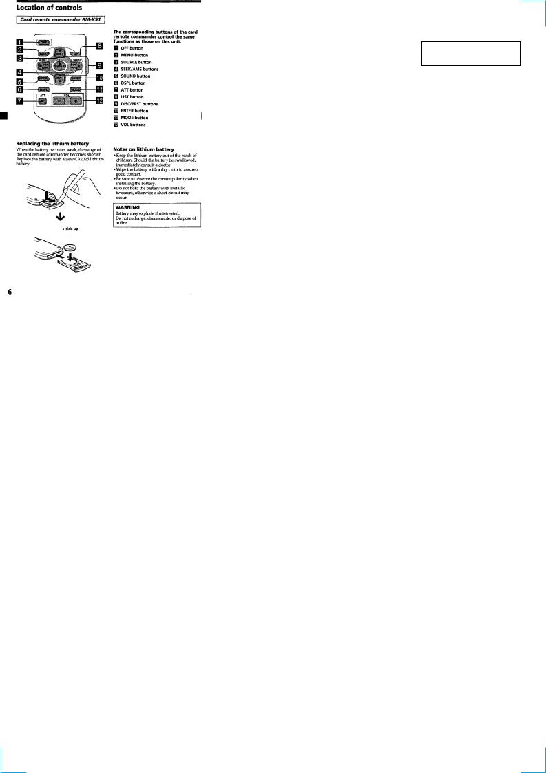
Card remote commander RM-X91 |
|||
Design and specifications are subject to change without notice.
FM/AM COMPACT DISC PLAYER
MICROFILM
1
Ver 1.1 2000. 08
SERVICE NOTES
CAUTION
Use of controls or adjustments or performance of procedures other than those specified herein may result in hazardous radiation exposure.
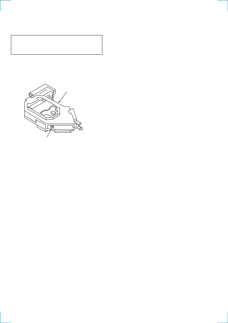
If the optical pick-up block is defective, please replace the whole optical pick-up block.
Never turn the semi-fixed resistor located at the side of optical pick-up block.
optical pick-up block
semi-fixed resistor
NOTES ON HANDLING THE OPTICAL PICK-UP BLOCK OR BASE UNIT
The laser diode in the optical pick-up block may suffer electrostatic breakdown because of the potential difference generated by the charged electrostatic load, etc. on clothing and the human body.
During repair, pay attention to electrostatic breakdown and also use the procedure in the printed matter which is included in the repair parts.
The flexible board is easily damaged and should be handled with care.
NOTES ON LASER DIODE EMISSION CHECK
The laser beam on this model is concentrated so as to be focused on the disc reflective surface by the objective lens in the optical pickup block. Therefore, when checking the laser diode emission, observe from more than 30 cm away from the objective lens.
Notes on Chip Component Replacement
•Never reuse a disconnected chip component.
•Notice that the minus side of a tantalum capacitor may be damaged by heat.
SAFETY-RELATED COMPONENT WARNING!!
COMPONENTS IDENTIFIED BY MARK 0 OR DOTTED LINE WITH MARK 0 ON THE SCHEMATIC DIAGRAMS AND IN
THE PARTS LIST ARE CRITICAL TO SAFE OPERATION. REPLACE THESE COMPONENTS WITH SONY PARTS WHOSE PART NUMBERS APPEAR AS SHOWN IN THIS MANUAL OR IN SUPPLEMENTS PUBLISHED BY SONY.
TABLE OF CONTENTS
1. GENERAL
Location of controls ................................................................. |
3 |
Getting Started ......................................................................... |
3 |
Setting the clock ...................................................................... |
3 |
CD Player CD/MD Unit (optional) ......................................... |
4 |
Radio ....................................................................................... |
5 |
Other Functions ....................................................................... |
6 |
TV/Video (optional) ................................................................ |
7 |
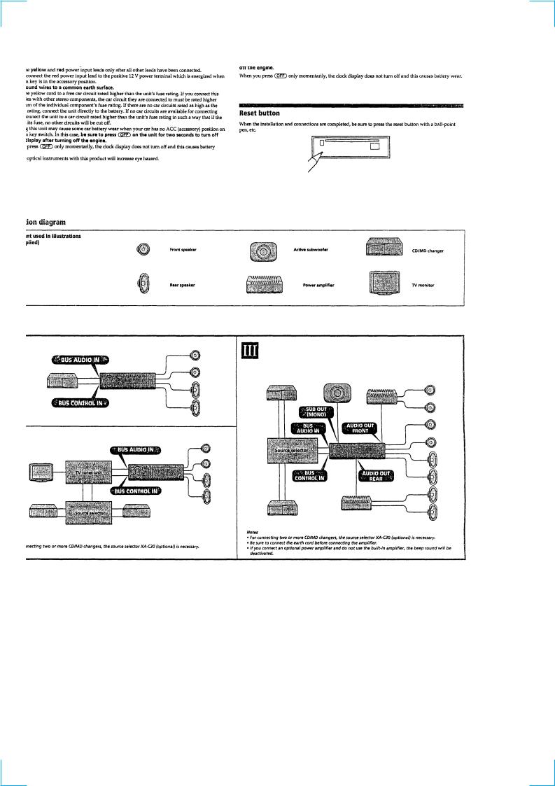
Connections ............................................................................. |
8 |
2. DISASSEMBLY
2-1. |
Sub Panel (CD) Assy ......................................................... |
10 |
2-2. |
CD Mechanism Block ....................................................... |
10 |
2-3. |
Main Board ....................................................................... |
11 |
2-4. |
Heat Sink ........................................................................... |
11 |
2-5. |
Chassis (T) Sub Assy ........................................................ |
12 |
2-6. |
Lever Section ..................................................................... |
12 |
2-7. |
Servo Board ....................................................................... |
13 |
2-8. |
Shaft Roller Assy .............................................................. |
13 |
2-9. |
Floating Block Assy .......................................................... |
14 |
2-10. |
Optical Pick-up Block ....................................................... |
14 |
3. DIAGRAMS
3-1. |
IC Pin Descriptions ........................................................... |
15 |
3-2. |
Block Diagram –CD Section– ........................................... |
21 |
3-3. |
Block Diagram –Tuner Section– ....................................... |
22 |
3-4. |
Block Diagram –Display Section– .................................... |
23 |
3-5. |
Circuit Boards Location .................................................... |
23 |
3-6. |
Printed Wiring Boards –CD Mechanism Section– ............ |
24 |
3-7. |
Schematic Diagram –CD Mechanism Section (1/2)– ....... |
26 |
3-8. |
Schematic Diagram –CD Mechanism Section (2/2)– ....... |
27 |
3-9. |
Schematic Diagram –Main Section (1/2)– ........................ |
28 |
3-10. |
Schematic Diagram –Main Section (2/2)– ........................ |
29 |
3-11. |
Printed Wiring Board –Main Section– .............................. |
30 |
3-12. |
Printed Wiring Board –Relay Section– ............................. |
31 |
3-13. |
Schematic Diagram –Relay Section– ................................ |
32 |
3-14. |
Schematic Diagram –Display Section– ............................. |
33 |
3-15. |
Printed Wiring Board –Display Section– .......................... |
34 |
3-16. |
IC Block Diagrams ............................................................ |
35 |
4. EXPLODED VIEWS
4-1. |
Chassis Section ................................................................. |
38 |
4-2. |
Front Panel Section ........................................................... |
39 |
4-3. CD Mechanism Section (1) ............................................... |
40 |
|
4-4. |
CD Mechanism Section (2) ............................................... |
41 |
4-5. |
CD Mechanism Section (3) ............................................... |
42 |
5. ELECTRICAL PARTS LIST ........................................ |
43 |
|
ATTENTION AU COMPOSANT AYANT RAPPORT
À LA SÉCURITÉ!!
LES COMPOSANTS IDENTIFIÉS PAR UNE MARQUE 0 SUR LES
DIAGRAMMES SCHÉMATIQUES ET LA LISTE DES PIÈCES SONT CRITIQUES POUR LA SÉCURITÉ DE FONCTIONNEMENT. NE REMPLACER CES COMPOSANTS QUE PAR DES PIÈCES SONY DONT LES NUMÉROS SONT DONNÉS DANS CE MANUEL OU DANS LES SUPPLÉMENTS PUBLIÉS PAR SONY.
2
SECTION 1 GENERAL
This section is extracted from instruction manual.
3
4

5
6
7
8

9
SECTION 2
DISASSEMBLY
Note : Follow the disassembly procedure in the numerical order given.
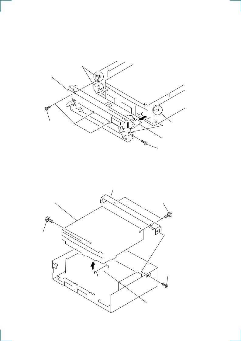
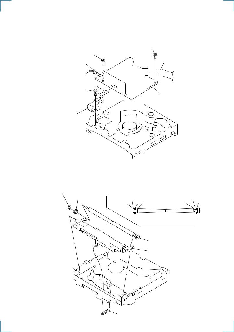
2-1. SUB PANEL (CD) ASSY
4 two claws
6 sub panel (CD) assy
2 PTT 2.6x6 |
3 claw |
5 CNP800
1 PTT 2.6x6
2-2. CD MECHANISM BLOCK
7 bracket (CD)
5 CD mechanism block |
6 PTT 2.6x6 |
2 PTT 2.6x6
3
1 PTT 2.6x6
4 CN301
10
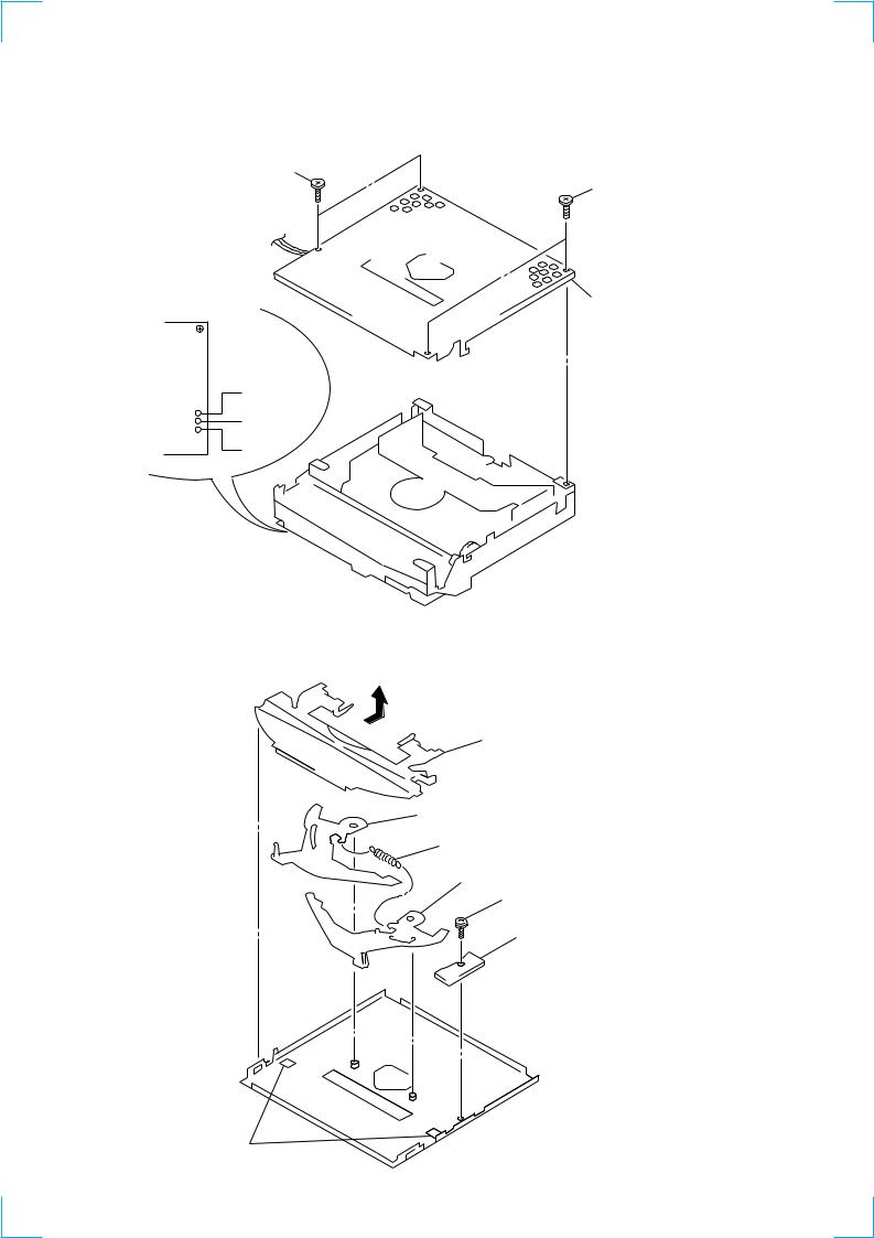
2-3. MAIN BOARD
4 PTT 2.6x6
6 MAIN board
5 PTT 2.6x6
3 PTT 2.6x8
2 PTT 2.6x8
1 PTT 2.6x8
2-4. HEAT SINK
7 heat sink
6 PTT 2.6x8
5 PTT 2.6x8
4 PTT 2.6x8
3 PTT 2.6x12
2 PTT 2.6x8
1 PTT 2.6x8
11
2-5. CHASSIS (T) SUB ASSY
2 P 2x3
3 P 2x3
1 Unsolder the
4 chassis (T) sub assy
lead wires.
black
red
white
2-6. LEVER SECTION
5 guide (disc)
6 lever (R)
3 tension spring (LR)
7 lever (L)
1 PS 2x3
2 DISC IN SW board
4 claws
12
2-7. SERVO BOARD
7 PS 2x4
6 PS 2x4
3 Removal the solders. |
2 CN2 |
|
1 CN3
4 P 2x3
8 SERVO board
5 loading motor assy
2-8. SHAFT ROLLER ASSY
•When installing, take note of the positions arm (roller) and washers. (Fig. 1)
3 retaing ring (RA)
4 shaft retainer
shaft retainer |
arm |
|
retaing ring (RA) arm washer |
washer |
shaft retainer |
Fig. 1
5 shaft roller assy
2 arm (roller)
1 tension spring (RA)
13
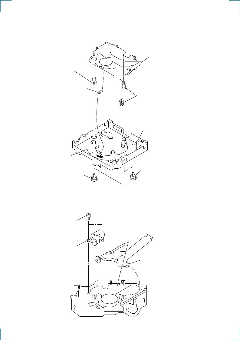
2-9. FLOATING BLOCK ASSY
6 floating block assy
7 compression spring (FL)
1 tension spring (KF1)
8 compression spring (FL)
4 Fit lever (D) in the direction of the arrow.
5 Turn loading ring in the direction of the arrow.
2 damper (T)
3 damper (T)
2-10. OPTICAL PICK-UP BLOCK
1 P 2x3
2 sled motor assy
3 optical pick-up block
14

SECTION 3
DIAGRAMS
3-1. IC PIN DESCRIPTIONS
• IC501 CXD2598Q (DIGITAL SERVO, DIGITAL SIGNAL PROCESSOR) (SERVO BOARD)
Pin No. |
Pin Name |
I/O |
Pin Description |
|
|
|
|
1 |
DVDD |
— |
Digital power supply pin |
|
|
|
|
2 |
DVSS |
— |
Digital ground |
|
|
|
|
3 |
SOUT |
O |
Servo brock serial data output (Not used.) |
|
|
|
|
4 |
SOCK |
O |
Servo brock serial data read clock output (Not used.) |
|
|
|
|
5 |
XOLT |
O |
Servo brock serial data latch output (Not used.) |
|
|
|
|
6 |
SQSO |
O |
Sub Q 80 bit, PCM peak and level data output. CD TEXT data output |
|
|
|
|
7 |
SQCK |
I |
Clock input from SQSO read output. |
|
|
|
|
8 |
SCSY |
I |
Fixed at “L”. |
|
|
|
|
9 |
SBSO |
O |
Serial output of sub-P to W. (Not used.) |
|
|
|
|
10 |
EXCK |
I |
Clock input from SBSO read output. (Fixed at “L”) |
|
|
|
|
11 |
XRST |
I |
System reset (“L”: Reset) |
|
|
|
|
12 |
STSM |
I |
System mute input (Fixed at “L”) |
|
|
|
|
13 |
DATA |
I |
Serial data input from CPU. |
|
|
|
|
14 |
XLAT |
I |
Latch input from CPU. Latch serial data at the falling edge. |
|
|
|
|
15 |
CLOK |
I |
Serial data transfer clock input from CPU. |
|
|
|
|
16 |
SENS |
O |
SENS output for CPU. |
|
|
|
|
17 |
SCLK |
I |
Clock input from SENS serial data read. |
|
|
|
|
18 |
ATSK |
I/O |
Input/output for anti-shock. |
|
|
|
|
19 |
WFCK |
O |
WFCK (Write Flame Clock) output (Not used.) |
|
|
|
|
20 |
XUGF |
O |
XUGF output (Not used.) |
|
|
|
|
21 |
XPCK |
O |
XPCK output (Not used.) |
|
|
|
|
22 |
GFS |
O |
GFS output |
|
|
|
|
23 |
C2PO |
O |
C2PO output (Not used.) |
|
|
|
|
24 |
SCOR |
O |
“H” output at either detection, sub code sync S0 or S1. |
|
|
|
|
25 |
C4M |
O |
4.2336 MHz output (Not used.) |
|
|
|
|
26 |
WDCK |
O |
Word clock input f=2Fs (Not used.) |
|
|
|
|
27 |
COUT |
I/O |
Track number count signal input/output (Not used.) |
|
|
|
|
28 |
MIRR |
I/O |
Mirror signal input/output (Not used.) |
|
|
|
|
29 |
DVSS |
— |
Digital ground |
|
|
|
|
30 |
DVDD |
— |
Digital power supply pin |
|
|
|
|
31 |
DFCT |
I/O |
Diffect signal input/output (Not used.) |
|
|
|
|
32 |
FOK |
I/O |
Focus OK signal output |
|
|
|
|
33 |
PWM1 |
I |
External control input of spindle motor. |
|
|
|
|
34 |
LOCK |
I/O |
Lock signal input/output |
|
|
|
|
35 |
MDP |
O |
Servo control output of spindle motor. |
|
|
|
|
36 |
SSTP |
I |
Disc most inner track detection signal input |
|
|
|
|
37 |
FSTIO |
I/O |
2/3 frequency division output of pins ih and ij. (Not used.) |
|
|
|
|
38 |
SFDR |
O |
Sled drive output |
|
|
|
|
39 |
SRDR |
O |
Sled drive output |
|
|
|
|
40 |
TFDR |
O |
Tracking drive output |
|
|
|
|
41 |
TRDR |
O |
Tracking drive output |
|
|
|
|
42 |
FFDR |
O |
Focus drive output |
|
|
|
|
43 |
FRDR |
O |
Focus drive output |
|
|
|
|
44 |
DVDD |
— |
Digital power supply pin |
|
|
|
|
45 |
DVSS |
— |
Digital ground |
|
|
|
|
46 |
TEST |
I |
Test pin (Fixed at “L”.) |
|
|
|
|
47 |
TES1 |
I |
Test pin (Fixed at “L”.) |
|
|
|
|
48 |
XTSL |
I |
X’tal select input (“L”: 16.9344 MHz, “H”: 33.8688 MHz) |
|
|
|
|
49 |
VC |
I |
Center voltage input |
|
|
|
|
50 |
FE |
I |
Focus error signal input |
|
|
|
|
51 |
SE |
I |
Sled error signal input |
|
|
|
|
15

Pin No. |
Pin Name |
I/O |
Pin Description |
|
|
|
|
52 |
TE |
I |
Tracking error signal input |
|
|
|
|
53 |
CE |
I |
Center servo analog input |
|
|
|
|
54 |
RFDC |
I |
RF signal input |
|
|
|
|
55 |
ADIO |
O |
Test pin (Not used.) |
|
|
|
|
56 |
AVSSO |
— |
Analog ground |
|
|
|
|
57 |
IGEN |
I |
Constant current input from OP amplifier. |
|
|
|
|
58 |
AVDDO |
— |
Analog ground |
|
|
|
|
59 |
ASYO |
O |
EFM full-swing output (“L”: VSS, “H”: VDD) |
|
|
|
|
60 |
ASYI |
I |
Asymmetry comparate voltage input |
|
|
|
|
61 |
RFAC |
I |
EFM signal input |
|
|
|
|
62 |
AVSS3 |
— |
Analog ground |
|
|
|
|
63 |
CLTV |
I |
VCO control voltage input from master. |
|
|
|
|
64 |
FILO |
O |
Filter output for master PLL (slave=digital PLL) |
|
|
|
|
65 |
FILI |
I |
Filter input from master PLL. |
|
|
|
|
66 |
PCO |
O |
Charge pump output for master PLL. |
|
|
|
|
67 |
AVDD3 |
— |
Analog power supply pin |
|
|
|
|
68 |
BIAS |
I |
Asymmetry circuit constant current input |
|
|
|
|
69 |
VCTL |
I |
VCO2 control input from wideband EFM PLL. (Not used.) |
|
|
|
|
70 |
V16M |
O |
VCO2 oscillator output for wideband EFM PLL. (Not used.) |
|
|
|
|
71 |
VPCO |
O |
Charge pump output for wideband EFM PLL. (Not used.) |
|
|
|
|
72 |
DVSS |
— |
Digital ground |
|
|
|
|
73 |
MD2 |
I |
Digital out ON/OFF control input (“L”: OFF, “H”: ON) |
|
|
|
|
74 |
DOUT |
O |
Digital out output |
|
|
|
|
75 |
ASYE |
I |
Asymmetry circuit ON/OFF input (“L”: OFF, “H”: ON) |
|
|
|
|
76 |
DVDD |
— |
Digital power supply pin |
|
|
|
|
77 |
LRCK |
O |
D/A interface LR clock output (f=Fs) |
|
|
|
|
78 |
LRCKI |
I |
D/A interface LR clock input |
|
|
|
|
79 |
PCMD |
O |
D/A interface serial data output (2’s COMP, MSB fast) |
|
|
|
|
80 |
PCMD |
I |
D/A interface serial data input (2’s COMP, MSB fast) |
|
|
|
|
81 |
BCK |
O |
D/A interface bit clock output |
|
|
|
|
82 |
BCKI |
I |
D/A interface bit clock input |
|
|
|
|
83 |
EMPH |
O |
Emphasis ON/OFF signal output |
|
|
|
|
84 |
EMPHI |
I |
Emphasis ON/OFF signal input (“H”: ON, “L”: OFF) |
|
|
|
|
85 |
XVDD |
— |
Power supply for master clock. |
|
|
|
|
86 |
XTAI |
I |
X’tal oscillator input from master clock (16.9344 MHz). |
|
|
|
|
87 |
XTAO |
O |
X’tal oscillator output for master clock (16.9344 MHz). |
|
|
|
|
88 |
XVSS |
— |
Ground pin for master clock. |
|
|
|
|
89 |
AVDD1 |
— |
Analog power supply pin |
|
|
|
|
90 |
AOUT1 |
O |
Lch analog output |
|
|
|
|
91 |
AIN1 |
I |
Lch OPAMP input |
|
|
|
|
92 |
LOUT1 |
O |
Lch LINE output |
|
|
|
|
93 |
AVSS1 |
— |
Analog ground |
|
|
|
|
94 |
AVSS2 |
— |
Analog ground |
|
|
|
|
95 |
LOUT2 |
O |
Rch LINE output |
|
|
|
|
96 |
AIN2 |
I |
Rch OPAMP input |
|
|
|
|
97 |
AOUT2 |
O |
Rch analog output |
|
|
|
|
98 |
AVDD2 |
— |
Analog power supply pin |
|
|
|
|
99 |
RMUT |
O |
Rch “0” detect Flug (Not used.) |
|
|
|
|
100 |
LMUT |
O |
Lch “0” detect Flug (Not used.) |
|
|
|
|
16
 Loading...