


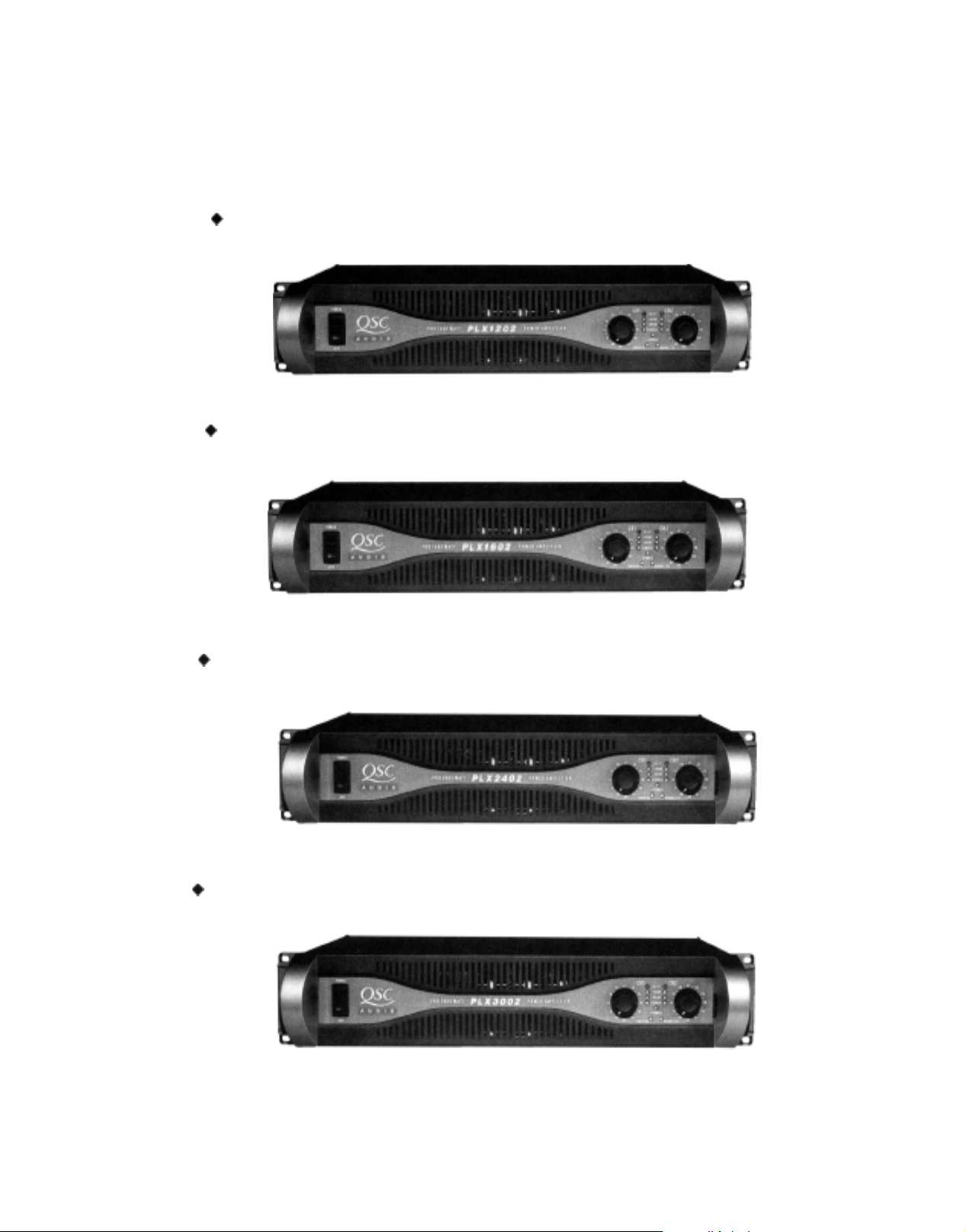
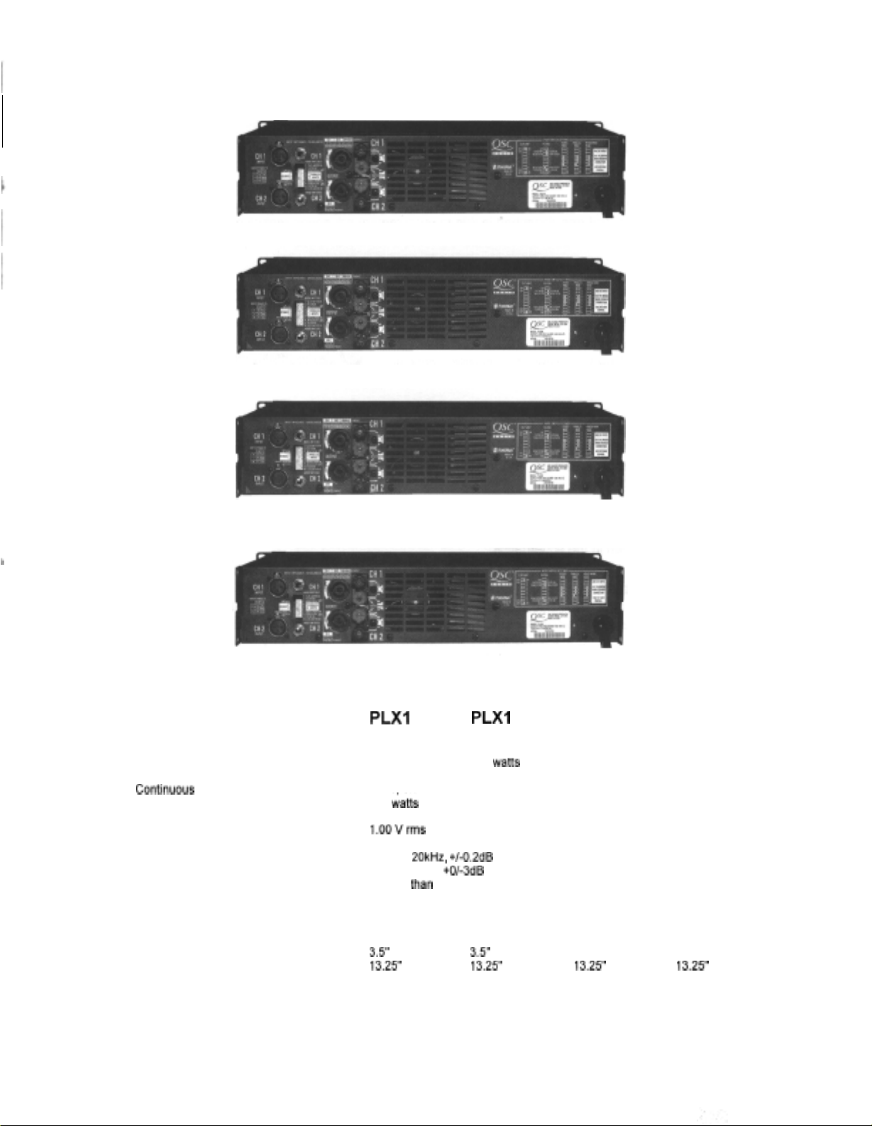
PLX-1202

Technical Service Manual
PLX™ Series
▲▲
▲▲
▲ PLX 1202
▲▲
▲▲
▲ PLX 1602
▲▲
▲▲
▲ PLX 2402
▲▲
▲▲
▲ PLX 3002
TD-000078-00
TD-000078-00
+
PLX
1202
+
PLX 1602
+
PLX 2402
+
PLX 3002

PLX SERIES
SERVICE MANUAL
PLX
1202
PLX 1602
PLX 2402
PLX 3002
QSC Technical Services
Wats: I
-%OO-772-2034
Local:
1-714-957-7150
Fax: 1-714-754-6173
QSC Technical Support BBS
I -714-668-7567
1-800-856-6003
QSC Audio Products, Inc.
1675 MacArthur Blvd.
Costa Mesa,
CA
92626
http://www.qscaudio.com

Table of Contents
PLX Product Specifications ................................................................
Introduction ........................................................................................
Test and Calibration ............................................................................
Troubleshooting PLX ...........................................................................
PLX Parts List
.....................................................
.....................................................
................................................
................................................
.....................................................
.....................................................
................................................
................................................
.....................................................
.....................................................
................................................
................................................
.....................................................
.....................................................
................................................
................................................
PLX Semiconductors ..............................................................................
Chassis Drawings ...................................................................................
Schematics
.....................................................
.....................................................
.....................................................
.....................................................
PLX Series PCB Circut Board Drawings .................................................
1
2
3
13
PLX 1202 PCB Assembly (120V) 23
PLX 1202 PCB Assembly (230V) 25
PLX 1202 Chassis Assembly (120V) 28
PLX 1202 Chassis Assembly (230V) 28
PLX 1602 PCB Assembly (120V) 28
PLX 1602 PCB Assembly (230V) 31
PLX 1602 Chassis Assembly (120V) 34
PLX 1602 Chassis Assembly (230V) 34
PLX 2402 PCB Assembly (120V) 35
PLX 2402 PCB Assembly (230V) 38
PLX 2402 Chassis Assembly (120V) 41
PLX 2402 Chassis Assembly (230V) 41
PLX 3002 PCB Assembly (120V) 42
PLX 3002 PCB Assembly (230V) 45
PLX 3002 Chassis Assembly (120V) 48
PLX 3002 Chassis Assembly (230V) 49
50
53
PLX 1202 Main PCB Schematics 57
PLX 1602 Main PCB Schematics 62
PLX 2402 Main PCB Schematics 67
PLX 3002 Main PCB Schematics 72
73
PLX Product Specifications
PLX
1202
PLX 1602
PLX 2402
PLX
3002
PLXI
202
PLXI
602
PLX2402
PLX3002
Output
Power (per channel):
Continuous Average
Output
Power both channels driven:
8
ohms,
2OHz
-
2OkHz,
0.03%
THD
200watts
4
ohms,
2OHz
-
2OkHz,
0.05%
THD
325
watts
Con0nuous
Average
Output
Power bridged mono
ooeration:
300
waKs
425watts 550
watts
500
watts
700
watts 900watts
8 ohms,
2OHz
-
2OkHz,
0.1% THD
Voltage Gain (dB)
Sensitivity (for rated power @ 8 ohms)
Distortion
Frequency Response (LF Switched Off)
Damping Factor (1
kHz
and Below)
Noise
Input
Impedance
Dimensions
Faceplate Width
Faceplate Height
Chassis Depth
Weight
Net,
Lbs/kg
700
iatts
1100
watts 1500 watts
32
32
32
1.00vrms
1.20 Vrms
1.50 Vrms
SMPTE-IM
Less
than
0.01%
2OHz
to
2OkHz,
+I-0.2dB
8Hz
to
5OkHz,
+Ol-3dB
Greater
than
500
106dB
below rated output (20 Hz
to
20 kHz)
6k unbalanced,
12k
balanced
2000 watts
32
1.70
vrms
Standard 19” Rack Mounting
3.Y
3.r
13.2Y
13.2v
2119.5 2119.5
3.5” 3.Y
13.2Y 13.2Y
2119.5
2119.5
Introduction
This manual is prepared to assist service personnel with the repair and calibration of PLX power
amplifiers
.
The procedures described in this manual require advanced technical experience
and sophisticated audio test equipment.
CAUTION: To reduce the risk of electric shock,
do not remove the cover. No user-serviceable
parts inside. Refer servicing to qualified
personnel.
CAUTION
WARNING: To prevent fire or electric shock, do
not expose this equipment to rain or moisture.
Documentation
This manual contains schematics, printed circuit board (PCB) drawings, parts lists, and
mechanical assembly drawings. This information should be used in conjunction with the
test and troubleshooting guide.
The electrical and electronic components are identified by circuit identification numbers on
the schematics and the parts list. The test
&
troubleshooting sections refer to
designations shown in the schematics.
Equivalent Parts
Although many of the electronic components used in this product may be available from
electronic suppliers, some components are specially tested and approved by
WC.
A
product repaired with
non-WC
supplied components may not meet factory specifications.
Repairs performed using non-QSC parts may void the product warranty.
men
in doubt,
you may contact
QSC
Technical Services for assistance.
Parts orders to QSC should include the product model number, the part description, and
the QSC part number (from the parts list in this manual). Parts will be shipped via UPS,
F.O.B. Costa Mesa, California. Shipping, handling and COD charges may be added to
the cost of the parts.
Factory Repair
It may become necessary to return a product to the factory for repair. Call QSC Technical
Services for return instructions. QSC Technical Services may be reached at (800)
772-2834.
Test and Troubleshooting Equipment
-
Distortion Analyzer capable of 0.01% THD+N
-
High Power Load Bank
(8,4,8
2
ohms)
-
Function Generator 8 Digital Multimeter
-
2OMHz
Oscilloscope
-
Variac (0-140
VAC,
30-40A)
-Audio
Precision
-
System One
+
Thermometer
2

Test
&
Calibration
PLX 1202 Test Procedure
.
SET-UP
1.
Connect a test load to the output terminals of the amplifier.
2. Make sure Mode Switches 1
-
10 are in the default position (1 on, 10 on, all others off).
3. Connect a distortion analyzer with a resolution of
O.Ol%,
20-2OkHz
(or better) to the
output terminals of the amplifier. Enable the
8OkHz
low pass filter.
4. Connect a dual-channel oscilloscope to the following test points:
Chl
-
a
IOX
(vertical sensitivity
-
2V/cm)
scope probe to the channel speaker output.
Ch2
-
a IX scope probe (vertical sensitivity
-
O.lV/cm)
to the distortion analyzer
output.
5.
Set amp gain pots fully clockwise and turn on power switch.
6. Connect the output of the signal generator to the input terminals of the amplifier and
select an output of 1.30
VRMS,
1
kHz
sine wave.
7. Plug the amplifier into a variac and set up an AC line current monitor.
. POWER UP 8 MUTE DELAY TEST
CAUTION: To avoid damage to the main printed circuit board, place a
50
ohm
225W
resistor (100 ohm,
240VAC) in series with the high
(+)
lead on the AC cable during variac ramp up. If the switching power
supply has a shorted device at initial power up, this AC resistor pad will help prevent undue damage. After
the amplifier has been fully powered up via the variac, confirm that the amplifier has achieved
stable operation during idle. Remove AC power from the amplifier and disconnect the series
resistor for normal operation. Continue with the test
&
calibration process.
I. Slowly raise the variac voltage and watch for excessive current draw (line current
greater than
0.5A
a.c. at 60 Volts). This is slightly less for 240V.
Pause at
9OVAC
(2OOVAC European) for three seconds until the mute I protect circuit disengages.
Continue to
12OVAC
(240V European).
2. Verify that the fan is operating at low speed.
3. Turn the power switch off and on a few times to verify the 3 second power-up muting
delay.
l CHANNEL OUTPUT
I. Look for amplified signal on the scope for channel
1.
Switch the input signal and scope
to channel 2 and repeat output test. Check for noisy
/
contaminated gain pots by
observing general instability on the distortion waveform while adjusting the gain control
levels.
2. Select an 8 ohm load and confirm that this amplifier is producing 200 watts at 1 kHz just
below the point of clipping. Check both channels.
l BRIDGE MODE
1. Turn the power switch off.
2. Set Mode Switch
#7
in the on position. The gain control, limiter, and filter switch positions
on CH2 are disabled with Mode Switch
#7
on.
3.
Set load to both red output binding posts
(CHI
positive and CH2 negative).
4. Apply a 1.30
VRMS,
1
kHz
sinewave input to channel I of the amplifier. Check the power
and verify that the output does not immediately collapse. Check for 700 watts at 8 ohms.

5.
Turn power off and place the amplifier back into the Stereo mode with output
loads connected to each channel.
. BIAS
1. Let the amplifier cool down to room temperature.
2. With an input amplitude of
1.3OVrms
increase the input frequency to
2OkHz.
Reduce the
input signal 20dB (80%) from full output. Adjust the crossover
trimpot
VR43
(CHl)
and
VR166 (CH2) for about a
4OOmVpk-pk
crossover spike protruding from the noise trace
on the oscilloscope. It will be necessary to have the oscilloscope measure unfiltered
distortion from the amplifier in order to see the crossover spike. It is necessary to
disable the 80kHz
lowpass
filter on the analyzer for this test.
Further trim so that
the total distortion for that channel is less than 0.1% THD+N.
3. With the trim settings achieved, and with no signal plugged into the amplifier and with an
8 ohm load, verify that the AC idle current from the AC service is no more than 1 .O
amperes.
4. Let the amplifier cool down and check channel 2.
. SHORT CIRCUIT CURRENT
1.
Select a 2 ohm load and apply a
1.3Vrms
sinewave (1
kHz)
input signal to both channels
of the amplifier.
Ensure that power is on and that the gain controls are fully up.
2. While the amplifier is producing power into the loads, apply a short to the output binding
posts of each channel. In other words, apply a jumper between the red and black
binding posts of each channel. Once this is done, combined AC line current draw for
both channels should be no greater than
13A
ac.
This is with a 120 volt AC service to
the amplifier. Current may be lower if AC line voltage is lower.
3. Remove the short from each channel and verify that the channels recover in to 2 ohm
loads. The output should not experience any hang up and a full
sinewave
should be
present just as it was before a short was applied for this test.
4. If the amplifier does not pass any of the above steps, troubleshoot the current limit
section of the amplifier. If steps 2, 3, and 4 above pass, continue to the next test
FREQUENCY RESPONSE.
l FREQUENCY RESPONSE
1,
Set load to 8 ohms and scale the input generator to gain 1 watt of power from the
amplifier on each channel. Gain controls on the amplifier should be fully up.
2.
Check frequency response from
2OHz
to 20kHz
(+I-
0.2OdB)
by sweeping random
frequencies between these extremes. This is done by verifying the same voltage
amplitude at each of the frequencies selected (within
2OHz
to
2OkHz).
Check both
channels.
l POWER vs. DISTORTION TEST
I. Check to ensure that both channels will produce rated power at
2OHz,
2KHz,
and 20kHz.
into an 8 ohm load.
2. While verifying rated power, check that at all frequencies the distortion measurement is
less than or equal to 0.03% THD.
l THERMAL TEST
1. Set input frequency to 1 KHz and short both channels while they are producing power into
a load.
2. Apply a short to the output of each channel.
3. AC line current draw should be about 11
-
13.5 amperes for both channels. As the
amplifier gets hot, there will be some current drift upwards and the fan speed will
increase. This is not a problem as long as the case temperature on the output
transistors does not exceed
105
degrees C.
4

4.
Verify that the NTC circuit causes thermal shutdown after an extended period.
5. When thermal shutdown occurs, verify AC idle current of less that 0.90 amperes
l CM TEST
1. Select an 8 ohm load and confirm that this amplifier is producing rated power.
2. Check the Common Mode of the amplifier by inserting a
1/4”
input jack halfway into each
channel and observe about 6
dB
of output voltage reduction. There will also be a 180
degree phase inversion at the output of the channel under test.
l OUTPUT NOISE
1. Set the amplifier gain controls all the way up, with a 1
kHz
1.3OVrms
sinewave
input
signal. Note the output level at full power just below clipping. Adjust gain if needed.
2. Remove the input signal connector from the amplifier and measure the residual noise
level produced into the load by the amplifier. The noise signal should be 107
dB
down
from the full output power point measured. A signal to noise ratio should be better than
or equal to
107dB.
Check both channels.
l FINAL CHECK
This completes the amplifier test procedure for this model.Inspect the amplifier for
mechanical defects. Inspect the solder connections. Reassemble the amplifier and verify
the amplifier’s operation before returning the product to service.
PLX 1602 Test Procedure
.
SET-UP
1.
2.
3.
4.
5.
6.
7.
Connect a test load to the output terminals of the amplifier.
Make sure Mode Switches 1
-
10 are in the default position (1 on, 10 on, all others off)
Connect a distortion analyzer with a resolution of
O.Ol%,
20-20kHz
(or better) to the
output terminals of the amplifier.Enable the 80kHz low pass filter.
Connect a dual-channel oscilloscope to the following test points:
Chl
-
a 1 OX (vertical sensitivity
-
2V/cm)
scope probe to the channel speaker output.
Ch2
-
a IX scope probe (vertical sensitivity
-
O.lV/cm)
to the distortion analyzer
output.
Set amp gain pots fully clockwise and turn on power switch.
Connect the output of the signal generator to the input terminals of the amplifier and
select an output of 1.30
VRMS,
1
kHz
sine wave.
Plug the amplifier into a variac and set up an AC line current monitor.
l POWER UP 8 MUTE DELAY TEST
CAUTION: To avoid damage to the main printed circuit board, place a
50
ohm 225W resistor (100 ohm,
240VAC) in series with the high
(+)
lead on the AC cable during variac ramp up. If the switching power
supply has a shorted device at initial power up, this AC resistor pad will help prevent undue damage. After
the amplifier has been fully powered up via the variac, confirm that the amplifier has achieved
stable operation during idle. Remove AC power from the amplifier and disconnect the series
resistor for normal operation. Continue with the test
&
calibration process.
Slowly raise the variac voltage and watch for excessive current draw (line current
greater than
0.5A
a.c
at 60 Volts).
T/I;s
is
s/;ghf/y
less
for 240V. Pause at
9OVAC
(2OOVAC
European) for three seconds until the mute
I
protect circuit disengages.
Continue to
12OVAC
(24OV
European).
Verify that the fan is operating at low speed.

3. Turn the power switch off and on a few times to verify the 3 second power-up muting
delay.
. CHANNEL OUTPUT
1. Look for amplified signal on the scope for channel 1. Switch the input signal and scope
to channel 2 and repeat output test. Check for noisy
/
contaminated gain pots by
observing general instability on the distortion waveform while adjusting the gain control
levels.
2. Select an 8 ohm load and confirm that this amplifier is producing 300 watts at 1 kHz just
below the point of clipping. Check both channels.
. BRIDGE MODE
1. Turn the power switch off.
2. Set Mode Switch
#7
in the on position. The gain control, limiter, and filter switch positions
on CH2 are disabled with Mode Switch
#7
on.
3. Set load to both red output binding posts
(CHI
positive and CH2 negative).
4. Apply a 1.30
VRMS,
1
kHz
sinewave input to channel 1 of the amplifier. Check the power
and verify that the output does not immediately collapse. Check for 1000 watts at 8
ohms.
5.
Turn power off and place the amplifier under test back into the Stereo mode with output
loads connected to each channel.
l BIAS
I. Let the amplifier cool down to room temperature.
2. With an input amplitude of
1.3OVrms
increase the input frequency to 20kHz. Reduce the
input signal 20dB (80%) from full output. Adjust the crossover
trimpot
VR43
(CHl)
and
VR166 (CH2) for about a
4OOmVpk-pk
crossover spike protruding from the noise trace
on the oscilloscope. It will be necessary to have the oscilloscope measure unfiltered
distortion from the amplifier in order to see the crossover spike.
It is necessary to
disable the 80kHz
lowpass
filter on the analyzer for this test. Further trim so that
the total distortion for that channel is less than 0.1% THD+N.
3. With the trim settings achieved, and with no signal plugged into the amplifier and with an
8 ohm load, verify that the AC idle current from the AC service is no more than 1 .O
amperes.
4. Let the amplifier cool down and check channel 2.
l SHORT CIRCUIT CURRENT
1.
Select a 2 ohm load and apply a
1.3Vrms
sinewave (1
kHz)
input signal to both channels
of the amplifier.Ensure that power is on and that the gain controls are fully up.
2. While the amplifier is producing power into the loads, apply a short to the output binding
posts of each channel.
In other words, apply a jumper between the red and black
binding posts of each channel. Once this is done, combined AC line current draw for
both channels should be no greater than
13A
ac. This is with a 120 volt AC service to
the amplifier. Current may be lower if AC line voltage is lower.
3. Remove the short from each channel and verify that the channels recover in to 2 ohm
loads. The output should not experience any hang up and a full
sinewave
should be
present just as it was before a short was applied for this test.
4. If the amplifier does not pass any of the above steps, troubleshoot the current limit
section of the amplifier. If steps 2, 3, and 4 above pass, continue to the next test
FREQUENCY RESPONSE.
6

l FREQUENCY RESPONSE
I.
Set load to 8 ohms and scale the input generator to gain 1 watt of power from the
amplifier on each channel. Gain controls on the amplifier should be fully up.
2. Check frequency response from
2OHz
to 20kHz
(+I-
0.2OdB)
by sweeping random
frequencies between these extremes. This is done by verifying the same voltage
amplitude at each of the frequencies selected (within
2OHz
to 20kHz). Check both
channels.
l POWER vs. DISTORTION TEST
1. Check to ensure that both channels will produce rated power at
2OHz,
2KHz,
and 20kHz.
into an 8 ohm load.
2.
While verifying rated power, check that at all frequencies the distortion measurement is
less than or equal to 0.03% THD.
l THERMAL TEST
1.
Set input frequency to 1 KHz and short both channels while they are producing power into
a load.
2. Apply a short to the output of each channel.
3. AC line current draw should be about
II
-
13.5 amperes for both channels. As the
amplifier gets hot, there will be some current drift upwards and the fan speed will
increase. This is not a problem as long as the case temperature on the output
transistors does not exceed 105 degrees
C.
4. Verify that the NTC circuit causes thermal shutdown after an extended period.
5. When thermal shutdown occurs, verify AC idle current of less that 0.90 amperes.
l CM TEST
1. Select an 8 ohm load and confirm that this amplifier is producing rated power.
2. Check the Common Mode of the amplifier by inserting a
1/4”
input jack halfway into each
channel and observe about 6
dB
of output voltage reduction. There will also be a 180
degree phase inversion at the output of the channel under test.
l OUTPUT NOISE
I. Set the amplifier gain controls all the way up, with a 1
kHz
1.3OVrms
sinewave
input
signal.
Note the output level at full power just below clipping. Adjust gain if needed.
2. Remove the input signal connector from the amplifier and measure the residual noise
level produced into the load by the amplifier. The noise signal should be 107
dB
down
from the full output power point measured. A signal to noise ratio should be better than
or equal to
107dB.
Check both channels.
l FINAL CHECK
This completes the amplifier test procedure for this model.
Inspect the amplifier for
mechanical defects. inspect the solder connections. Reassemble the amplifier and
veri@
the amplifier’s operation before returning the product to service.
PLX 2402 Test Procedure
l SET-UP
1. Connect a test load to the output terminals of the amplifier.
2. Make sure Mode Switches 1
-
10
are in the default position (1 on, 10 on, all others off).

3. Connect a distortion analyzer with a resolution of
O.Ol%,
20-20kHz
(or better) to the
output terminals of the amplifier. Enable the 80kHz low pass filter.
4. Connect a dual-channel oscilloscope to the following test points:
Chl
-
a
1OX
(vertical sensitivity
-
2V/cm) scope probe to the channel speaker output.
Ch2
-
a IX scope probe (vertical sensitivity
-
0.
IV/cm)
to the distortion analyzer
output.
5. Set amp gain pots fully clockwise and turn on power switch.
6. Connect the output of the signal generator to the input terminals of the amplifier and
select an output of 1.50
VRMS
1
kHz
sine wave.
7. Plug the amplifier into a variac and set up an AC line current monitor.
l POWER UP
&
MUTE DELAY TEST
CAUTION: To avoid damage to the main printed circuit board, place a
50
ohm
225W
resistor (100 ohm,
240VAC) in series with the high
(+)
lead on the AC cable during variac ramp up. if the switching power
supply has a shorted device at initial power up, this AC resistor pad will help prevent undue damage. After
the amplifier has been fully powered up via the variac, confirm that the amplifier has achieved
stable operation during idle. Remove AC power from the amplifier and disconnect the series
resistor for normal operation. Continue with the test
&
calibration process.
1. Slowly raise the variac voltage and watch for excessive current draw (line current
greater than
0.5A
a.c
at 60 Volts).
This
is
slight/y
/ess
fof
24OV.
Pause at
9OVAC
(2OOVAC
European) for three seconds until the mute
/
protect circuit disengages.
Continue to
12OVAC
(24OV
European).
2. Verify that the fan is operating at low speed.
3.
Turn the power switch off and on a few times to verify the 3 second power-up muting
delay.
l CHANNEL OUTPUT
I. Look for amplified signal on the scope for channel
1.
Switch the input signal and scope
to channel 2 and repeat output test. Check for noisy
/
contaminated gain pots by
observing general instability on the distortion waveform while adjusting the gain control
levels.
2. Select an 8 ohm load and confirm that this amplifier is producing 425 watts at 1 kHz just
below the point of clipping. Check both channels.
l BRIDGE MODE
1. Turn the power switch off.
2. Set Mode Switch
#7
in the on position. The gain control, limiter, and filter switch positions
on CH2 are disabled with Mode Switch
#7
on.
3. Set load to both red output binding posts
(CHI
positive and CH2 negative).
4. Apply a 1.30
VRMS,
1
kHz
sinewave
input to channel 1 of the amplifier. Check the power
and verify that the output does not immediately collapse. Check for 1500 watts at 8
ohms.
5. Turn power off and place the amplifier under test back into the Stereo mode with output
loads connected to each channel.
l BIAS
1.
Let the amplifier cool down to room temperature.
2. With an input amplitude of
1.5OVrms,
increase the input frequency to
2OkHz.
Reduce the
input signal 20dB (80%) from full output. Adjust the crossover
trimpot
VR43
(CHl)
and
VR166 (CH2) for about a
4OOmVpk-pk
crossover spike protruding from the noise trace
on the oscilloscope. It will be necessary to have the oscilloscope measure unfiltered
distortion from the amplifier in order to see the crossover spike.
It is necessary to

disable the 80kHz
lowpass
filter on the analyzer for this test.Further trim so that
the total distortion for that channel is less than 0.1%
THD+N,
3. With the trim settings achieved, and with no signal plugged into the amplifier and with an
8 ohm load, verify that the AC idle current from the AC service is no more than 1 .O
amperes.
4. Let the amplifier cool down and check channel
2.
l SHORT CIRCUIT CURRENT
1.
Select a 2 ohm load and apply a
1.3Vrms
sinewave (1
kHz)
input signal to both channels
of the amplifier.Ensure that power is on and that the gain controls are fully up.
2. While the amplifier is producing power into the loads, apply a short to the output binding
posts of each channel. In other words, apply a jumper between the red and black
binding posts of each channel. Once this is done, combined AC line current draw for
both channels should be no greater than
13A
ac. This is with a 120 volt AC service to
the amplifier. Current may be lower if AC line voltage is lower.
3. Remove the short from each channel and verify that the channels recover in to 2 ohm
loads. The output should not experience any hang up and a full
sinewave
should be
present just as it was before a short was applied for this test,
4. If the amplifier does not pass any of the above steps, troubleshoot the current limit
section of the amplifier. If steps 2, 3, and 4 above pass, continue to the next test
FREQUENCY RESPONSE.
l FREQUENCY RESPONSE
1. Set load to 8 ohms and scale the input generator to gain 1 watt of power from the
amplifier on each channel. Gain controls on the amplifier should be fully up.
2. Check frequency response from
2OHz
to 20kHz
(+/-
0.2OdB)
by sweeping random
frequencies between these extremes. This is done by verifying the same voltage
amplitude at each of the frequencies selected (within
2OHz
to 20kHz). Check both
channels.
l POWER vs. DISTORTION TEST
1. Check to ensure that both channels will produce rated power at
2OHz,
2KHz,
and 20kHz.
into an 8 ohm load.
2. While verifying rated power, check that at all frequencies the distortion measurement is
less than or equal to 0.03%
THD.
l THERMAL TEST
1. Set input frequency to 1 KHz and short both channels while they are producing power into
a load.
2. Apply a short to the output of each channel.
3. AC line current draw should be about
11
-
13.5 amperes for both channels. As the
amplifier gets hot, there will be some current drift upwards and the fan speed will
increase, This is not a problem as long as the case temperature on the output
transistors does not exceed 105 degrees C.
4. Verify that the NTC circuit causes thermal shutdown after an extended period.
5,
When thermal shutdown occurs, verify AC idle current of less that 0.90 amperes.
l CM TEST
I. Select an 8 ohm load and confirm that this amplifier is producing rated power.
2. Check the Common Mode of the amplifier by inserting a
114”
input jack halfway into each
channel and observe about 6
dB
of output voltage reduction. There will also be a 180
degree phase inversion at the output of the channel under test.
9

l OUTPUT NOISE
1. Set the amplifier gain controls all the way up, with a I
kHz
1.5OVrms
sinewave
input
signal.
Note the output level at full power just below clipping. Adjust gain if needed.
2. Remove the input signal connector from the amplifier and measure the residual noise
level produced into the load by the amplifier. The noise signal should be 107
dB
down
from the full output power point measured. A signal to noise ratio should be better than
or equal to
107dB.
Check both channels.
l FINAL CHECK
This completes the amplifier test procedure for this model.Inspect the amplifier for
mechanical defects. Inspect the solder connections. Reassemble the amplifier and verify
the amplifier’s operation before returning the product to service,
PLX 3002 Test Procedure
l SET-UP
1. Connect a test load to the output terminals of the amplifier.
2. Make sure Mode Switches 1
-
10 are in the default position
(1
on, 10 on, all others off).
3.
Connect a distortion analyzer with a resolution of
O.Ol%,
20-20kHz
(or better) to the
output terminals of the amplifier. Enable the 80kHz low pass filter.
4. Connect a dual-channel oscilloscope to the following test points:
Chl
-
a
1OX
(vertical sensitivity
-
2V/cm)
scope probe to the channel speaker output.
Ch2
-
a
1X
scope probe (vertical sensitivity
-
O.lV/cm)
to the distortion analyzer
output.
5.
Set amp gain pots fully clockwise and turn on power switch.
6. Connect the output of the signal generator to the input terminals of the amplifier and
select an output of 1.70
VRMS,
1
kHz
sine wave.
7. Plug the amplifier into a variac and set up an AC line current monitor.
. POWER UP 8 MUTE DELAY TEST
CAUTION: To avoid damage to the main printed circuit board, place a
50
ohm 225W resistor (100 ohm,
240VAC) in series with the high
(+)
lead on the AC cable during variac ramp up. If the switching power
supply has a shorted device at initial power up, this AC resistor pad will help prevent undue damage. After
the amplifier has been fully powered up via the variac, confirm that the amplifier has achieved
stable operation during idle. Remove AC power from the amplifier and disconnect the series
resistor for normal operation. Continue with the test
&
calibration process.
1.
Slowly raise the variac voltage and watch for excessive current draw (line current
greater than
0.5A
a.c. at 60 Volts).
TIG.s
is
s/ight/y
less for
24UV.
Pause at
9OVAC
(2UOVAC
European) for three seconds until the mute
/
protect circuit disengages.
Continue to
12OVAC
(240V European).,
2. Verify that the fan is operating at low speed.
3. Turn the power switch off and on a few times to verify the 3 second power-up muting
delay.
l CHANNEL OUTPUT
1.
Look for amplified signal on the scope for channel 1. Switch the input signal and scope
to channel 2 and repeat output test. Check for noisy I contaminated gain pots by
observing general instability on the distortion waveform while adjusting the gain control
levels.
10

2. Select an 8 ohm load and confirm that this amplifier is producing
550
watts at 1 kHz just
below the point of clipping. Check both channels.
l BRIDGE MODE
1. Turn the power switch off.
2. Set Mode Switch
#7
in the on position. The gain control, limiter, and filter switch positions
on CH2 are disabled with Mode Switch
#
7 on.
3. Set load to both red output binding posts
(CHI
positive and CH2 negative).
4. Apply a 1.30
VRMS,
1
kHz
sinewave input to channel 1 of the amplifier. Check the power
and verify that the output does not immediately collapse. Check for 2000 watts at 8
ohms.
5. Turn power off and place the amplifier under test back into the Stereo mode with output
loads connected to each channel.
l BIAS
1.
Let the amplifier cool down to room temperature.
2. With an input amplitude of
1.7OVrms
increase the input frequency to 20kHz. Reduce the
input signal 20dB
(80°h)
from full output. Adjust the crossover
trimpot
VR43
(CHI)
and
VRl66
(CH2) for about a
4OOmVpk-pk
crossover spike protruding from the noise trace
on the oscilloscope. It will be necessary to have the oscilloscope measure unfiltered
distortion from the amplifier in order to see the crossover spike. It is necessary to
disable the 80kHz
lowpass
filter on the analyzer for this test.Further trim so that
the total distortion for that channel is less than 0.1% THD+N.
3,
With the trim settings achieved, and with no signal plugged into the amplifier and with an
8 ohm load, verify that the AC idle current from the AC service is no more than 1 .O
amperes.
4. Let the amplifier cool down and check channel
2.
l SHORT CIRCUIT CURRENT
1.
Select a 2 ohm load and apply a
1.3Vrms
sinewave (1
kHz)
input signal to both channels
of the amplifier.Ensure that power is on and that the gain controls are fully up.
2,
While the amplifier is producing power into the loads, apply a short to the output binding
posts of each channel. In other words, apply a jumper between the red and black
binding posts of each channel. Once this is done, combined AC line current draw for
both channels should be no greater than
13A
ac. This is with a 120 volt AC service to
the amplifier. Current may be lower if AC line voltage is lower.
3. Remove the short from each channel and verify that the channels recover in to 2 ohm
loads. The output should not experience any hang up and a full
sinewave
should be
present just as it was before a short was applied for this test.
4. If the amplifier does not pass any of the above steps, troubleshoot the current limit
section of the amplifier. If steps 2, 3, and 4 above pass, continue to the next test
FREQUENCY RESPONSE.
l FREQUENCY RESPONSE
1. Set load to 8 ohms and scale the input generator to gain I watt of power from the
amplifier on each channel. Gain controlson the amplifier should be fully up.
2. Check frequency response from
2OHz
to 20kHz
(+I-
0.2OdB)
by sweeping random
frequencies between these extremes. This is done by verifying the same voltage
amplitude at each of the frequencies selected (within
2OHz
to 20kHz). Check both
channels.
11

l POWER vs. DISTORTION TEST
1.
Check to ensure that both channels will produce rated power at
2OH2,
2KHz,
and 20kHz.
into an 8 ohm load.
2. While verifying rated power, check that at all frequencies the distortion measurement is
less than or equal to 0.03% THD.
l THERMAL TEST
I. Set input frequency to
1 KHz and short both channels while they are producing power into
a load.
2. Apply a short to the output of each channel.
3. AC line current draw should be about 11
-
13.5 amperes for both channels. As the
amplifier gets hot, there will be some current drift upwards and the fan speed will
increase. This is not a problem as long as the case temperature on the output
transistors does not exceed 105 degrees
C.
4. Verify that the NTC circuit causes thermal shutdown after an extended period.
5. When thermal shutdown occurs, verify AC idle current of less that 0.90 amperes.
l CM TEST
1. Select an 8 ohm load and confirm that this amplifier is producing rated power.
2. Check the Common Mode of the amplifier by inserting a
114”
input jack halfway into each
channel and observe about
6
dB
of output voltage reduction. There
will
also be a 180
degree phase inversion at the output of the channel under test.
l OUTPUT NOISE
1. Set the amplifier gain controls all the way up, with a 1
kHz
1.7OVrms
sinewave
input
signal.
Note the output level at full power just below clipping. Adjust gain if needed.
2. Remove the input signal connector from the amplifier and measure the residual noise
level produced into the load by the amplifier. The noise signal should be 107
dB
down
from the full output power point measured. A signal to noise ratio should be better than
or equal to
107dB.
Check both channels.
l FINAL CHECK
This completes the amplifier test procedure for this model.
Inspect the amplifier for
mechanical defects. Inspect the solder connections. Reassemble the amplifier and verify
the amplifier’s operation before returning the product to service.
12
T r o ubleshooting
PLX 1202 l PLX 1602 l PLX 2402 l PLX 3002
Power Supply
-
-
Replacing Blown
IGBTs.
In order to improve
EMI
performance, reduce cost, and increase current capacity, the PLX
IGBTs
are driven by an active, direct coupled integrated circuit, rather than a gate drive transformer.
IGBT
or
driver failure should be rare (when correctly assembled) but when the
IGBT’s
blow, it usually damages the
following parts:
CHECKLIST AFTER BLOWN
IGBT’S
Q96, Q97,
(IGBT’s
generally fail in pairs)
D78, D79,
R358,
R359,
gate drive coupling
comonents,
check after removing blown
IGBT’s.
Ul8,
lR2110
high-side gate driver, Fault current when low-side
IGBT
shorts to upper rail. Such currents
also typically damage the gate coupling parts noted above.
Ul9,
3525 controller, Blows from currents shorted
thru
Ul8,
or possibly by overvoltage on the supply rail
SOMETIMES
Ul4,
556,
powered from
5V
output of 3525, which may fail high when 3525 fails.
RARELY
Ul3,
which has fairly high supply voltage ratings.
PROBABLE CAUSES OF MASSIVE
IGBT
FAULTS
SHORTS IN CONTROL CIRCUIT.
The parts operate well within their ratings and should hold up well in the field. The usual cause of failure is
when both
IGBT’s
turn on at once, shorting Pri-Hi to Pri-Lo. This occurs when something causes the drive
signal to one part to remain on when the other part is supposed to turn on. Shorts from solder or debris are
one obvious cause.
SHORTS IN THE LOAD.
Although there is peak current shutdown, shorts in the power amplifier transistors or secondary-side supply
components can cause currents to increase too quickly to prevent damage.
OVERVOLTAGE ON THE BIAS SUPPLY.
If the TOP-210 bias supply fails to operate, no harm occurs, the unit simply does not operate.
However, open circuit (missing part) in several key components can cause the Bias supply voltage to be
much too high, This blows the 2110 and thus the
IGBT’s.
QUICK TEST OF BIAS SUPPLY.
Ramp the AC voltage up slowly to 25% of regular voltage (30V for
12OV
unit). If the bias supply is working
normally, the green “power” LED should come on between 30 and
35Vz
with its usual, steady
“half-brighr
start-up level. If the LED comes on at
2OV,
or not until
5OV,
or blinks, DO NOT RAISE VOLTAGE PAST 60V
until you have measured the bias voltage. The switching will not start until you reach
9OV,
so you can save
the
IGBT’s
from blowing.
Confirm that bias voltage at Cl38 is
18-19V.
Open or missing
D63,
64, 65, 66, 67 or R349 will break the
feedback to U16 and cause overvoltage.
13
Troubleshooting “TOP-210” Bias Supply.
QUICK TEST OF BIAS SUPPLY.
Ramp the AC voltage up slowly to 25% of regular voltage (30V for
12OV
unit). If the bias supply is working
normally, the green “power” LED should come on between 30 and
35V,
with its usual, steady
“half-brighf’
start-up level.
CAUTION: if the LED comes on at
2OV,
or not until
5OV,
or blinks, DO NOT RAISE VOLTAGE PAST 60V
until you have measured the bias voltage. The switching will not start until you reach
9OV,
so you can save
the
IGBT’s
from blowing.
Confirm that bias voltage at Cl38 is
18-19V.
BIAS SUPPLY VOLTAGE MUCH TOO HIGH
D63,64,65,66,67
or R349 open or missing -- breaks feedback to U16
NO BIAS SUPPLY VOLTAGE
U16 missing or blown.
Tl missing, reversed, or open primary
D62 open or missing.
BIAS VOLTAGE ERRORS
The exact voltage is controlled by the feedback through
D63,
64_
65, 66, 67 and R349 as follows:
Cl38 is the
“+18V’
rail with about
18.8V
typical.
D63,
64, 65 each subtract a diode drop
(0.7V)
from Cl38.
Cl39
,
is the
“+16V”
rail with about
16.6V
typcial.
D66,
a
IOV
zener
diode
,
plus diode
D67,
subtract about 1 IV from
+16.6V.
R349 subtracts about
0.5V,
bringing the net voltage at
Ul6,
feedback pin 4, to about
5.lV.
Ul6
uses this feedback to adjust the “on” time at pin 5, in order
toraise
or lower the
flyback
voltage
charging Cl38 and thus maintain regulation of the
+16V
and
+18V
supplies
C142,
R356,
and R349 form a closed-loop stability circuit which prevents the regulated voltage from
“hunting”.
Q99
and associated R374 reduce the voltage of the Bias supply by 33% when the AC voltage is turned off.
This prevents the Power LED from showing at half brightness after turn-off, since U16 continues to run
from the main filters for some time after shut down R375 and 376 sense the output of
Ul3:3,
the “Loss of
AC” comparator, and cause
Q99
to turn on. If
Q99
is shorted, the bias voltages will remain 33% low when
AC is turned on.
REPLACING BLOWN TOP-210.
If U16 has blown, check T-l for continuity after removing
Ul6.
Its primary may be open. Pins I-2 It should
measure about 15 ohms
Replacing Blown Output Transistors
OUTPUT TRANSISTOR SHORTED
Stmrk
in one device tend to cause the opposing device to blow as
well,
If an output transistor shorts:
Drive transistor will be shorted
(Q26,
Q27,
Q71,
Q72)
CXNne
transistors will short in pairs (Q39
&
Q40,
Q36
&
Q37,
Q84
8
Q85,
Q81
8,
Q82)
The rest will short in fours
(Q28,
Q29,
Q34
&
Q35;
Q73,
Q74,
Q79
8,
Q80)
IGBT’s
8 their associated components may
fail
14
CHECK EMITTER AND BASE RESISTORS WHILE DEVICES ARE REMOVED,
Each output transistor has an associatated pair of 0.47 ohm resistors in parallel.
Each BANK of output transistors has a 15 ohm resistor from base to rail (emitter bus).
Audio Outputs, Troubleshooting Current Limit
WEAK CURRENT LIMIT -- PREMATURE CLIPPING.
The usual symptom of weak output current is premature clipping of one or more peaks of the audio voltage.
This could be caused by missing step, weak current limit, or dead output section.
PREMATURE CLIPPING at 60% VOLTAGE, SIMILAR AT ALL IMPEDANCES:
This points to a step problem (2402, 3002 only). See Step Troubleshooting.
If the amplifier reaches full voltage at 8 ohms, but prematurely clips at 4 ohms or 2 ohms, we can assume
the step is OK but the output current is too low (see below).
NO OUTPUT AT ALL ON ONE POLARITY.
This indicates complete failure (open circuit) in the circuit leading to the dead output polarity. Check the
series components in the current splitter for missing or open:
Ch 1:
Positive,
Ql9,
R381,
Q20,
R70,
DIO,
D14. Negative:
Q22,
R382,
Q21,
R71,
Dl
I,
D12
Ch 2:
Positive,
Q64,
R383,
Q65,
Rl93,
D35,
D39. Negative:
Q67,
R384,
Q66,
Rl94,
D36,
D37
CONSTANT, PREMATURE CLIPPING, WORSE AT LOW IMPEDANCES.
First, check the clamping voltages on
C21
(Ch
I+),
C22 (Ch I-),
C56
(Ch
2+),
C57
(Ch
2-),
as shown in
table below. At idle, all four voltages should all be similar. If one is out, check parts according to the
following table
CLAMPING VOLTAGES ARE WRONG AT IDLE
CHANNEL-POLARITY
Measure voltage on:
3002 and 2402, about
6V.
1602, about
4,6V,
1202 about
4.9V.
Voltage too high: missing resistor:
or missing transistor:
Voltage
0-0.3V:
shorted transistor
or missing resistor
Voltage
0.7V,
missing resistor:
Voltage wrong: wrong value
CH
I+
CH
l-
c21
c22
R60
Q14
Ql4,24
R
51,
72
R59
R59,60
R61
Ql5
Ql5,
25
R53,
75
R62
R62,61
CH
2+
C56
RI83
Q59
Q59,69
Rl74,
195
RI82
Rl82,
183
CH
2-
c57
RI84
Q60
Q60,70
Rl76,
198
RI85
Rl85,184
The exact voltage varies with temperature. Look for the mismatching value on the weak cell.
A too-low voltage causes early clamping of that output section, as explained in the previous several pages.
If the voltage is correct and current is still low, also check for missing
-
unsoldered output device, or emitter
resistors.
15
Audio Power Stage, Current Limit Troubleshooting
CURRENT LIMITS WHICH COLLAPSE PREMATURELY.
An immediate collapse of ALL current limits at full power could be premature triggering of “Power Supply
Cutback”, which is described in the section below. Cutback after several seconds of full power operation at
two ohms is normal.
Cutback of one or more output sections, at full temperature, while approaching full power into two ohms is
also normal. However, cutbacks at 4 ohms, or when cold into two ohms, indicate problems with the
transistor power measuring circuitry.
CLAMPING VOLTAGES COLLAPSE TOO SOON.
CHANNEL-POLARITY
CH
I+
CH
l-
CH
2+
CH
2-
Measure voltage on:
c21
c22
C56
c57
Cuts back too easily: low value,
R67,
73
R68,
74
Rl90,
196
Rl91,
197
or high value:
R
51,
72
R53,
75
Rl74,
195
Rl76,
198
or missing diode:
D9
D8
D34
D33
CLAMPING VOLTAGES ARE CORRECT, CURRENT STILL WEAK.
Shorted diode
DIO,
14
Dll,
12
D35,
39
D36,
37
Missing-unsoldered output device or emitter resistor.
TROUBLESHOOTING “POWER SUPPLY CUTBACK”.
As noted in the section on Power Supply, the amplifier’s current limit cuts back when necessary to protect
the power supply. Because the Observed effect is a reduced output voltage, in response to prolonged
operation above the long-term current limit, we commonly refer to this behavior as “power supply cutback”,
but we must remember that it is actually
amp/Tier
current
hmifhg
in response to an overload signal sent
from the power supply. Full power operation into 2 ohms (both channels) should produce a 50% cutback of
current after several seconds.
If both channels of the amplifier fail to cut back after about 3 seconds, 2-ohms, both channels driven, the
cutback signal is probably missing. CAUTION: Prolonged operation under these conditions could blow
IGBT
or burn out
Cl44.
Test for 6-10 seconds maximum.
Check the output (secondary side) pins of U17 (sh 4). Confirm presence of
+6V
on pin
5.
Pin 4 should
normally be at about
OV,
and go high (I-5V) after 3 seconds at full power,
If
Ul7-pin
4 does not go high, check U17 itself. If it appears OK, trace the circuitry driving U17 (PRIMARY
SIDE, CAUTION). Check for continuity through
L6:2
to Pri-Lo, check missing or open
R343,
D61,
Q95,
R347,
all of which drive optocoupler U17. A short in R346 or Cl31 will also prevent drive to U17.
If
Ul7-pin
4 goes high on schedule, and BOTH channels fail to cut back, trace voltage on
“PS_OL”
bus to
R273 (sh
3),
which connects to “MUTE+” bus. Continue tracing voltage on MUTE+ to
Ql6
(sh I) and
Q61
(sh 2). If only ONE channel fails to cut back, look for missing
Ql6,
R 65,
Ql7
(sh I) or
Q61,
Rl88,
Q62
(sh 2).
Cl31 controls the speed of cutback.. If missing, the amplifier current limits will enter cutback almost
immediately at or above full power, 4 ohms.
SHORT CIRCUIT CURRENT DOESN’T CUT BACK.
CAUTION: DO NOT MAINTAIN A SHORTED LOAD IF CUTBACK FAILS TO OCCUR WITHIN 1 SECOND.
It will be necessary to measure the output current with a DC current probe, or by noting the voltage across
a low value resistance with a DC scope, in order to determine which output cell is failing to cut back.
Failure to cut back could indicate either lack of clamping, or lack of voltage cutback. Measure the voltage
on the respective clamp capacitor. If the voltage decreases, but current limiting does not cut back, check
the clamping transistor.
:
16
CLAMPING VOLTAGE DECREASES, BUT NO CURRENT CUTBACK
CHANNEL-POLARITY CH
I+
CH
l-
CH
2+
CH
2-
Measure voltage on:
c21
c22
C56
C5?
Check clamp transistor
Q18
Q23
Q63 Q68
If the measured voltage on the clamp capacitor is not decreasing to about 50% during the short, check the
circuitry which measures the current during short circuit,
CLAMPING VOLTAGE DOES NOT DECREASE TO 50% DURING SHORT.
CHANNEL-POLARITY
CH
I+
CH
l-
CH
2+
CH
2-
Measure voltage on:
c21
c22
C56
c57
Missing cutback transistor, resistor
Q24,
R67
Q25,
R68
Q69,
RI90
Q70,
RI91
Missing voltage sense resistor,
R 73 R 74
RI96 RI97
Shorted or low value shunt resistor R72
R75
RI95
RI98
Troubleshooting Thermal Tracking
MOUNTING PROBLEMS WITH IOK SENSING NTC.
The thermal sensing for fan and bias tracking depends on a 1 OK NTC which is mounted in a hole in the
heat sink. The hole is filled with thermal grease to improve coupling. If the NTC is not straight while
mounting the heat sink, it may short out against the side of its hole. It is mounted on a standoff which
protrudes into the hole, so this should not occur if care is taken while installing the heatsink.
If shorted to the heat sink, the amplifier output voltage is coupled to the NTC. If the short is to the grounded
lead of the
NTC,
it may not damage anything. If to the other end, a large voltage is put across the NTC
which will probably damage it.
SHORT FROM “LIVE” END OF NTC TO HEAT SINK:
Replace affected NTC
BE AWARE! This can short (relatively) quietly and then appear to be operating normally. Poor bias
tracking can indicate this problem. Sometimes this short will not happen until the amplifier is driven past IV
input.
NTC BENT OVER AND SHORTED TO DRIVER TRANSISTORS.
May touch
Ql9,
Q26,
or
Q64,
Q71.
This causes severe overcurrent to the affected output cell, possibly damaging the parts in series with the
shorted transistor. It may also blow the power supply.
Replace affected
NTC,
drive transistors, check components in series with drive transistor
Ch 1:
Ql9
shorted, check,
R381,
Q20,
R70,
DIO,
D14.
Q26 shorted, check ALL outputs and opposing driver transistor on this channel.
Ch 2:
Q64 shorted, check
R383,
Q65,
Rl93,
D35,
D39.
Q71
shorted, check ALL outputs and opposing driver transistor on this channel.
17

Audio Output, Troubleshooting Stability Feedback
HIGH FREQUENCY OSCILLATIONS
SEVERE-DRAWS CURRENT-GROSS DISTORTION
C27 (62) missing or wrong, or series R367 (368)
C 25, 26 (60, 61) missing
Secondary filter capacitors missing or open (unlikely that ALL are defective).
SEVERE, BUT DOES NOT DRAW LARGE CURRENT
R22 (146) open.
MARGINAL -- MAY APPEAR ONLY AS EXCESS DISTORTION
Cl4 (49) missing
Cl 6 (50) missing or too large
C28 (63) missing
C 25 or 26 (60 or 61) missing or too large
Cl95 or 196 missing (input board).
EXCESSIVE OSCILLATION JUST BELOW CLIPPING, 2-4 ohms
Cl 7 (52) missing
NOTE: about 0.1% oscillation right below clipping at 2 ohms is normal.
EXCESSIVE SWITCHING INTERFERENCE.
Switching interference may LOOK like an instability, however it is at a much lower frequency
(1lOkH.z)
than
most instabilities. It will be more visible at low frequencies
(2OOHz)
and at lower impedances.
Missing jumper at
R224.
Missing
Cl29,
134 on output board.
Grounds not connected to chassis at output board and front chassis mounting screw.
FEEDBACK PROBLEMS: GAIN INCORRECT
Gain of output stage set by
R23,
31 (147, 153)
Gain of Ch 1 volume control buffer stage set by RI
1,
16.
Gain of Ch 2 volume control buffer stage set by
Rl37,
139. Make sure
Q48
is turned on
-
grounding
RI37
at Q48 should not affect gain. Check RI 32 (drives Q48).
Gain of balanced input is set by 4 matched resistors
R9,
8, 12, 13 (129, 130, 135, 136). Confirm both sides
of balanced input are working. Check
R5,
6 (123, 124).
Audio Output, Troubleshooting Clipping, Limiting
EXCESS STICKING (TOO MUCH DISTORTION DURING CLIP LIMITING)
Cl4 (49) much too large (also causes increased high frequency distortion).
R38 (161) missing.
R38-39
(161-162) have wrong values.
Q9,
10 (54, 55) missing
R34 (157) or
R35
(158) missing
Q8
(53) missing
18

CLIP LIMITING DOESN’T WORK:
BOTH CHANNELS:
Check U3 missing,
Check U3 supply voltages, +I
3VCL,
-13VCL,
on
C73*
74
ONLY ONE CHANNEL BAD:
Probe output of U2
(7),
pin 7 while clipping. If output exceeds 4V during clipping, check
:
R38 (161) missing.
R38-39
(161-162)
have wrong values.
Q9,
10 (54, 55) missing.
R34 (157) or
R35
(158) missing
Q8 (53) missing
If output at pin 7 clamps at
3.5.4V
as expected, check parts surrounding U3:
R32 (154) missing
Q7 (52) missing
R28 (151) missing
Q6 (51) missing
RI8
(141) missing
RI9 (142) missing
SW I:1 (1:lO) not making contact
Check each pin on U3
CLIP LIMITING OSCILLATES:
Cl 3 (48) missing.
R21,
27 (144, 150) missing
Troubleshooting Step Problems
EXCESSIVE STEP DISTORTION (STEP GLITCH)
Close scrutiny of the distortion trace, and scope probing of the switched waveform, will help determine the
cause of excess step distortion, The step should switch when the output voltage is within IO-12 volts of its
respective rail, This switching margin should be fairly constant from
20-
20kHz. The switching event itself
should be a fairly uniform up and down ramp, moving at about 25 volts/us, therefore taking about
2us
to
complete its transition.
Step Switching Too Close
to
the
Rail:
This will cause increased step glitch, especially at low impedances. If present at all frequencies,
check the reference voltages:
Negref: 17.5 volts above its intermediate rail:
D88,
R276-7-8.
PosRef:
20V below its intermediate rails:
D87,
R256,
257,
D53.
Confirm correct values in output voltage divider: R48 loaded by
R49-50
(Rl71,
and
Rl72-173).
If present
only at high frequencies, check the value of the speed up capacitor
C20
(C55)
in the output voltage divider,
or look for slow switching (see below).
19

Step Chattering.
If the step repeatedly switches on and off, usually at a low frequency, it creates an oscillation burst
which increases step glitch at low frequency. The tendency is usually worse at low impedances
and low frequencies. 2-3 “false trials” at very low frequency, 2 ohms, is normal, but prolonged
bursts of maximum frequency chattering may cause FET failure.
Positive step: check hysteresis resistor R66 (RI 89)
Negative step: check hysteresis resistor R69 (RI 92) and capacitor Cl 87 (Cl 93).
Slow or Fast Switching.
Slow switching reduces step glitch but puts more strain on the FET. Fast switching increases step
glitch. The usable limit is
17-27
volts/us,
If both slopes are equally off speed, check the slope capacitors:
Positive,
C30
(C65)
and Negative, C29 (C64).
If only one slope is slow, check the resistors and buffer transistors:
Positive step:
R78,
79,
Dl5,
Q30-31
(R201,
202,
D40,
Q7576)
Negative step:
R83,
84,
Dl7,
Q32-33
(R206,
207,
D42,
Q77-78).
Step FET Oscillation.
Certain FET types oscillate at extremely high frequency while ramping up and down. This injects
interference into the amplifier which increases the step glitch. Such problems are supposed to be
found while
(dis)qualifying
specific FET types. If they crop up in production, Engineering needs to
know.
STEP WON’T TURN ON (Premature Clipping)
If the step refuses to switch high, the amp will clip prematurely, at the intermediate rail, at any load. Make
sure the clipping is not
acually
current cutback, usually evident only at 2 ohms. Probe the output voltage
and intermediate rail voltages to confirm clip point and lack of step action. Trace the circuit from the step
FET back via gate drive to drive circuit to locate cracks, missing part etc. Check DC power on step driver
(14V
on EACH positive step drivers,
12V
on BOTH negative drivers). Check voltage of
PosRef
(20V below
+65V
rail) or Negref
(17.5V
above
-65V
rail). Look for severe mismatches of the comparator resistor
ladders.
STEP STUCK ON (Switched Rail Voltage Stuck On Full)
If the positive step is stuck on, (evidenced by permanent high voltage on switched rail) the FET is probably
bad, since the positive gate drive cannot sustain DC turn-on due to the bootstrapping. If the negative step
is stuck on, it could be a bad
FET,
or the gate drive circuit could be holding the FET on, which will easily be
confirmed by measuring the gate voltage. Malfunctioning gate drive circuitry should be checked as noted
above under “Won’t Turn On”.
REPEATED FET FAILURE.
Repeated failure of step
FET’s
is usually caused by failure to fully switch ON or OFF (lingering in the linear
region). The actual failure usually occurs at 2 ohms, where the dissipation is highest. After replacing the
FET,
the step waveform should be monitored, starting at light load to avoid repeated failure, and advancing
briefly to heavier loads while closely watching the waveform. You will need to use an isolated scope probe
which allows voltage readings to be taken with respect to the intermediate rails, or to FET sources.
FET Does Not Fully Turn On:
Generally causes problems at low frequency, 2 ohms.
Confirm that the step FET remains fully on for the entire cycle
(2OHz).
If not, confirm weak gate
drive and determine cause.
Weak positive drive: check voltage on C32
(C51)
for
14V.
Check
C31
(C66),
low RIO4
(R227),
missing D18
(Dl48).
Check
R78,
Dl5,
Q30
(R201,
D40,
Q75).
Weak negative drive: check voltage on
C67,
12V.
Check
R83,
Dl7,
Q32
(R206,
D42,
Q77).
20
FET Turns On or Off Very Slowly:
Generally causes problems at high frequency, 2 ohms.
If both slopes are equally slow, check the slope capacitors:
Positive,
C30
(035)
and Negative, C29 (034).
If only one slope is slow, check the resistors and buffer transistors:
Positive step:
R78,
79,
Dl5,
Q30-31
(R201,
202,
D40,
Q75-76)
Negative step:
R83,
84,
Dl7,
Q32-33
(R206,
207,
D42,
Q77-78).
Severe Step Oscillation.
Generally observed at low frequency, low impedance, right at threshold.
Positive step: check hysteresis resistor
R66
(RI 89)
Negative step: check hysteresis resistor
R69
(RI 92) and capacitor Cl 87 (Cl 93)
Troubleshooting DC Fault Shutdown
NORMAL BEHAVIOR OF THE CIRCUIT.
Any amplifier fault which causes a non-symmetrical output, such as premature clipping of one polarity, a
missing step,
etc,
may trigger DC fault shutdown. This indicates normal operation of the circuit
TRACING THE CAUSE OF FALSE TRIGGERS.
If amplifier is shutting down for no apparent cause, the source of the false signal must be found. Be sure the
output is checked with a DC coupled scope in order to confirm absence of an actual DC offset. The circuit
will trip on DC offsets exceeding about
4V.
The optocoupler’s input can be safely disabled by shorted
Ul5,
pins I-2 together. This will indicate if false
triggering is before or after
Ul5.
The output of
UlO:l,
pin 1 should be monitored. If it goes low during DC shutdown, it is sending the false
signal.
SHUTDOWN OCCURS AS SOON AS SWITCHING STARTS.
Disable
Ul5
as noted above, determine if there is a DC fault condition. CAUTION: use
50-ohm
resistor in
series with AC line to limit fault current in case of shorted outputs.
If amplifier output looks OK, check UlO:l output. If low, check voltage on pins 2 and 3
UlO:l,
pin 2: should be zero (no signal)
UlO:l,
pin
31
should be about
2V!
set by
R243,
244, 245.
Check R348 at Ul.5.
SHUTDOWN OCCURS ABOVE ABOUT 4V OUTPUT:
Q87,
C7,
R240
or D48 missing.
Confirm D48 is pulled low
(-13V),
holding Q87 on. If not, check RI 17, 118, Q42
NOTE: this control voltage responds to the Br Mono switch, pole
7.
Check R348 at
Ul5.
Bad connection at step diodes
(D21,
D22,
D46,
D47)
21
 Loading...