


 Loading...
ORDER NO.
RRV3568
XV-DV363
DVD/CD RECEIVER
XV-DV363
XV-DV365K
THIS MANUAL IS APPLICABLE TO THE FOLLOWING MODEL(S) AND TYPE(S).
Model |
Type |
|
|
|
|
Power Requirement |
Regional restriction codes |
Remarks |
||||
|
|
|
|
(Region No.) |
||||||||
|
|
|
|
|
|
|
|
|
|
|
|
|
|
|
|
|
|
|
|
|
|
|
|
|
|
XV-DV363 |
WYXJ5 |
AC 220 V to 240 V |
2 |
|
||||||||
|
|
|
|
|
|
|
|
|
|
|
|
|
XV-DV365K |
WXJ/RE5 |
AC 220 V to 240 V |
5 |
|
||||||||
|
|
|
|
|
|
|
|
|
|
|
|
|
|
|
|
|
|
|
|
|
|
|
|
|
|
|
|
|
|
|
|
|
|
|
|
|
|
|
|
|
|
|
|
|
|
|
|
|
|
|
|
|
|
|
|
|
|
|
|
|
|
|
|
|
|
|
|
|
|
|
|
|
|
|
|
|
|
|
|
|
|
|
|
|
|
|
|
|
|
|
|
|
|
|
|
|
|
|
|
|
|
|
|
For details, refer to "Important Check Points for good servicing".
PIONEER CORPORATION 4-1, Meguro 1-chome, Meguro-ku, Tokyo 153-8654, Japan
PIONEER ELECTRONICS (USA) INC. P.O. Box 1760, Long Beach, CA 90801-1760, U.S.A.
PIONEER EUROPE NV Haven 1087, Keetberglaan 1, 9120 Melsele, Belgium
PIONEER ELECTRONICS ASIACENTRE PTE. LTD. 253 Alexandra Road, #04-01, Singapore 159936
 PIONEER CORPORATION 2007
T-IZK APR. 2007 printed in Japan
|
1 |
|
2 |
|
3 |
|
4 |
|
|
|
|
|
|
SAFETY INFORMATION
A
This service manual is intended for qualified service technicians ; it is not meant for the casual do- it-yourselfer. Qualified technicians have the necessary test equipment and tools, and have been trained to properly and safely repair complex products such as those covered by this manual. Improperly performed repairs can adversely affect the safety and reliability of the product and may void the warranty. If you are not qualified to perform the repair of this product properly and safely, you should not risk trying to do so and refer the repair to a qualified service technician.
B |
WARNING! |
|
The laser component is capable of emitting radiation exceeding |
||
|
||
|
the limit for CLASS 1. A specially instructed person should do |
|
|
servicing operation of the apparatus. |
|
|
|
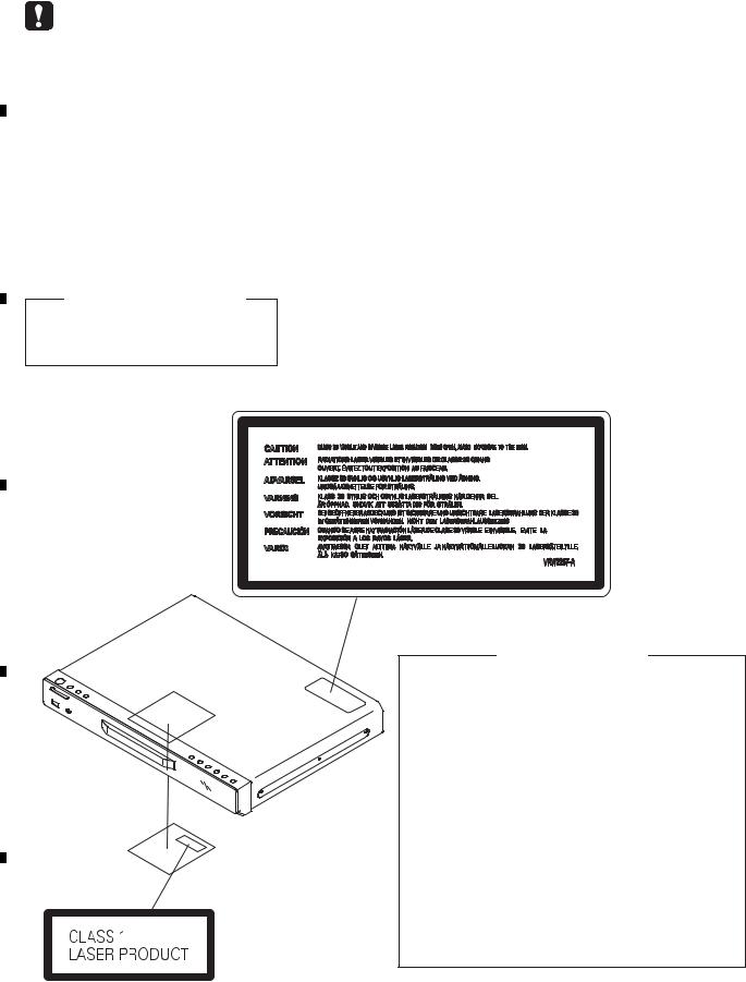
LASER DIODE CHARACTERISTICS
FOR DVD : MAXIMUM OUTPUT POWER : 5 mW
WAVELENGTH : 650 nm
FOR CD : MAXIMUM OUTPUT POWER : 7 mW
WAVELENGTH : 780 nm
C LABEL CHECK
D
E
Name Label
F
VRW2257
Additional Laser Caution
1.Laser Interlock Mechanism
•Loading switch (S101 on the LOAB Assy) is used for interlock mechanism of the laser.
When this switch turned ON in SW2 (CLOSE) side (OPEN signal is 0 V and CLOSE signal is 3.5 V), a laser becomes the status which can completely oscillation.
Furthermore, the laser completely oscillates in the disc judgment and disc playback.
When player is power ON state and laser diode is not completely oscillating, 780 nm laser diode is always oscillating by half power.
•Laser diode is driving with Q307 (650 nm LD) and Q308 (780 nm LD) on the DVD MAIN Assy.
Therefore, when short-circuit between the emitter and collector of these transistors or the base voltage is supplied for transistors turn on, the laser oscillates. (failure mode)
•In the test mode , there is the mode that the laser oscillates except for the disc judgment and playback. LD ON mode in the test mode oscillates with the laser forcibly.
The interlock mechanism mentioned above becomes invalid in this mode.
2.When the cover is open, close viewing through the objective lens with the naked eye will cause exposure to the laser beam.
: Refer to page 25.
2 |
|
|
|
|
|
|
|
|
|
|
|
|
XV-DV363 |
|
|
|
|
||||
|
1 |
|
2 |
|
|
|
3 |
|
4 |
|
|
|
|
|
|
|
|
||||

|
5 |
|
6 |
|
7 |
|
8 |
|
|
|
|
|
|
A
B
C
D
E
F
|
|
|
|
|
|
|
|
3 |
|
|
|
|
|
|
XV-DV363 |
|
|
||||
|
|
|
|
|
|
|
|
|||
|
5 |
|
6 |
|
|
|
7 |
|
8 |
|
|
|
|
|
|
|
|
||||
|
1 |
|
|
2 |
|
|
3 |
|
|
4 |
|
|
|
|
|
|
|||||||
|
CONTENTS |
|
|
|
|
|
|
|
|
||
|
SAFETY INFORMATION..................................................................................................................................... |
|
|
|
|
|
|
2 |
|
||
|
1. SERVICE PRECAUTIONS............................................................................................................................... |
|
|
|
|
|
|
5 |
|
||
A |
1.1 NOTES ON SOLDERING .......................................................................................................................... |
|
|
|
|
|
|
5 |
|
||
1.2 CAUTION |
|
|
|
|
|
|
5 |
|
|||
|
|
|
|
|
|
|
|
||||
|
2. SPECIFICATIONS............................................................................................................................................ |
|
|
|
|
|
|
6 |
|
||
|
2.1 SPECIFICATIONS and ACCESORRIES ................................................................................................... |
|
|
|
6 |
|
|||||
|
2.2 PANEL FACILITIES.................................................................................................................................... |
|
|
|
|
|
|
7 |
|
||
|
3. BASIC ITEMS FOR SERVICE........................................................................................................................ |
|
|
|
|
|
|
10 |
|
||
|
3.1 CHECK POINTS AFTER SERVICING..................................................................................................... |
|
|
|
10 |
|
|||||
|
|
|
|
|
|||||||
|
.....................................................................................................................................3.2 PCB LOCATIONS |
|
|
|
|
|
|
11 |
|
||
|
3.3 JIGS LIST ................................................................................................................................................ |
|
|
|
|
|
|
12 |
|
||
|
3.4 CLEANING............................................................................................................................................... |
|
|
|
|
|
|
12 |
|
||
|
4. BLOCK DIAGRAM.......................................................................................................................................... |
|
|
|
|
|
|
14 |
|
||
|
4.1 OVERALL WIRING CONNECTION DIAGRAM and LOAB ASSY |
........................................................... |
|
|
14 |
|
|||||
B |
4.2 OVERALL BLOCK DIAGRAM.................................................................................................................. |
|
|
|
|
|
|
16 |
|
||
|
5. DIAGNOSIS.................................................................................................................................................... |
|
|
|
|
|
|
18 |
|
||
|
5.1 METHOD FOR DIAGNOSING DEGRADATION OF THE LDS ON THE PICKUP................................... |
18 |
|
||||||||
|
5.2 DVD TROUBLE SHOOTING ................................................................................................................... |
|
|
|
|
|
|
19 |
|
||
|
5.3 CIRCUIT DESCRIPTION OF DIGITAL AMP. SECTION .......................................................................... |
|
|
|
22 |
|
|||||
|
5.4 SPECIFICATIONS FOR THE PROTECTION CIRCUITS FOR THE .....................DIGITAL AMPLIFIER |
23 |
|
||||||||
|
5.5 PASS/FAIL TEST PROCEDURE OF HDMI TRANSMITTER IC |
|
|
|
24 |
|
|||||
|
|
|
|
|
|||||||
|
............................................................................................................................................6. SERVICE MODE |
|
|
|
|
|
|
25 |
|
||
|
6.1 TEST MODE ............................................................................................................................................ |
|
|
|
|
|
|
25 |
|
||
|
6.2 DISPLAY SPECIFICATION OF THE TEST MODE.................................................................................. |
|
|
|
26 |
|
|||||
|
6.3 FUNCTIONAL SPECIFICATION OF THE SHORTCUT KEY .................................................................. |
|
|
|
27 |
|
|||||
|
6.4 SPECIFICATION OF MODEL INFORMATION DISPLAY ........................................................................ |
|
|
|
28 |
|
|||||
C |
6.5 FUNCTIONAL SPECIFICATION OF THE SERVICE MODE ................................................................... |
|
|
|
29 |
|
|||||
|
6.6 SERVICE TEST MODE ........................................................................................................................... |
|
|
|
|
|
|
30 |
|
||
|
7. DISASSEMBLY .............................................................................................................................................. |
|
|
|
|
|
|
33 |
|
||
|
8. EACH SETTING AND ADJUSTMENT ........................................................................................................... |
|
|
|
|
|
|
40 |
|
||
|
8.1 ADJUSTMENT......................................................................................................................................... |
|
|
|
|
|
|
40 |
|
||
|
8.2 ID NUMBER AND ID DATA SETTING ..................................................................................................... |
|
|
|
45 |
|
|||||
|
..........................................................................................................9. EXPLODED VIEWS AND PARTS LIST |
|
|
|
|
|
|
48 |
|
||
|
|
|
|
|
|
|
|
||||
|
9.1 PACKING SECTION ................................................................................................................................ |
|
|
|
|
|
|
48 |
|
||
|
9.2 EXTERIOR SECTION.............................................................................................................................. |
|
|
|
|
|
|
50 |
|
||
|
9.3 06 LOADER ASSY................................................................................................................................... |
|
|
|
|
|
|
52 |
|
||
|
9.4 TRAVERSE MECHANISM ASSY-S ......................................................................................................... |
|
|
|
|
|
|
54 |
|
||
D |
10. SCHEMATIC DIAGRAM............................................................................................................................... |
|
|
|
|
|
|
56 |
|
||
10.1 DVD MAIN ASSY (1/5) |
|
|
|
|
|
|
56 |
|
|||
|
|
|
|
|
|
|
|
||||
|
10.2 DVD MAIN ASSY (2/5) .......................................................................................................................... |
|
|
|
|
|
|
58 |
|
||
|
10.3 DVD MAIN ASSY (3/5) .......................................................................................................................... |
|
|
|
|
|
|
60 |
|
||
|
10.4 DVD MAIN ASSY (4/5) .......................................................................................................................... |
|
|
|
|
|
|
62 |
|
||
|
10.5 DVD MAIN ASSY (5/5) .......................................................................................................................... |
|
|
|
|
|
|
64 |
|
||
|
10.6 DAMP ASSY (1/2).................................................................................................................................. |
|
|
|
|
|
|
66 |
|
||
|
|
|
|
|
|
|
|
||||
|
..................................................................................................................................10.7 DAMP ASSY (2/2) |
|
|
|
|
|
|
68 |
|
||
|
10.8 DISPLAY, USB, LED and KEY ASSYS .................................................................................................. |
|
|
|
70 |
|
|||||
|
10.9 MIC ASSY (XV-DV365K ONLY)............................................................................................................. |
|
|
|
|
|
|
72 |
|
||
|
10.10 EUROSCART ASSY............................................................................................................................ |
|
|
|
|
|
|
74 |
|
||
|
10.11 POWER SUPPLY UNIT ....................................................................................................................... |
|
|
|
|
|
|
76 |
|
||
E |
10.12 WAVEFORMS...................................................................................................................................... |
|
|
|
|
|
|
78 |
|
||
|
11. PCB CONNECTION DIAGRAM.................................................................................................................... |
|
|
|
|
|
|
80 |
|
||
|
11.1 LOAB ASSY ........................................................................................................................................... |
|
|
|
|
|
|
80 |
|
||
|
11.2 MIC ASSY (XV-DV365K ONLY) ............................................................................................................. |
|
|
|
|
|
|
81 |
|
||
|
11.3 DVD MAIN ASSY ................................................................................................................................... |
|
|
|
|
|
|
82 |
|
||
|
11.4 DAMP ASSY .......................................................................................................................................... |
|
|
|
|
|
|
86 |
|
||
|
11.5 DISPLAY, USB, LED and KEY ASSYS |
|
|
|
88 |
|
|||||
|
|
|
|
|
|||||||
|
.........................................................................................................................11.6 POWER SUPPLY UNIT |
|
|
|
|
|
|
90 |
|
||
|
11.7 EUROSCART ASSY .............................................................................................................................. |
|
|
|
|
|
|
92 |
|
||
|
12. PCB PARTS LIST......................................................................................................................................... |
|
|
|
|
|
|
93 |
|
||
F
4 |
|
|
|
|
|
|
|
|
|
|
|
|
XV-DV363 |
|
|
|
|
||||
|
1 |
|
2 |
|
|
|
3 |
|
4 |
|
|
|
|
|
|
|
|
||||

|
5 |
|
6 |
|
7 |
|
8 |
|
|
|
|
1. SERVICE PRECAUTIONS
1.1 NOTES ON SOLDERING
•For environmental protection, lead-free solder is used on the printed circuit boards mounted in this unit.
Be sure to use lead-free solder and a soldering iron that can meet specifications for use with lead-free solders for repairs accompanied by reworking of soldering.
•Compared with conventional eutectic solders, lead-free solders have higher melting points, by approximately 40 °C. Therefore, for lead-free soldering, the tip temperature of a soldering iron must be set to around 373 °C in general, although the temperature depends on the heat capacity of the PC board on which reworking is required and the weight of the tip of the soldering iron.
Do NOT use a soldering iron whose tip temperature cannot be controlled.
Compared with eutectic solders, lead-free solders have higher bond strengths but slower wetting times and higher melting temperatures (hard to melt/easy to harden).
The following lead-free solders are available as service parts:
•Parts numbers of lead-free solder: GYP1006 1.0 in dia.
GYP1007 0.6 in dia. GYP1008 0.3 in dia.
A
B
1.2 CAUTION
NOTES ON BTL DRIVE
C
As a signal to drive the BTL is output from the negative speaker terminal, DO NOT short-circuit between the negative speaker terminal and ground, such as the chassis.
Do not short-circuit between the plus speaker terminal and ground, such as the chassis, too.
D
Negative Speaker Terminal
Do not short-circuit
 Ground (Chassis)
E
F
|
|
|
|
|
|
|
|
5 |
|
|
|
|
|
|
XV-DV363 |
|
|
||||
|
|
|
|
|
|
|
|
|||
|
5 |
|
6 |
|
|
|
7 |
|
8 |
|
|
|
|
|
|
|
|
||||

|
1 |
|
2 |
|
3 |
|
4 |
|
|
|
|
|
|
2. SPECIFICATIONS
2.1 SPECIFICATIONS and ACCESORRIES
A
B
C
(XV-DV363)
(XV-DV365K)
D
 Accessories
E |
• Power Cord (ADG1127) |
• FM Antenna (ADH7030) |
• Video Cable |
• Remote Control |
|
|
|
(L = 1.5 m) (XDE3046) |
(XV-DV363 : XXD3121) |
|
|
|
|
(XV-DV365K : XXD3124) |
|
• AM Loop Antenna |
• Dry Cell Battery (AA/R6) |
|
||
|
(ATB7013) |
|
F
6 |
|
|
|
|
|
|
|
|
|
|
|
|
XV-DV363 |
|
|
|
|
||||
|
1 |
|
2 |
|
|
|
3 |
|
4 |
|
|
|
|
|
|
|
|
||||
|
5 |
|
6 |
|
7 |
|
8 |
|
|
|
|
|
|
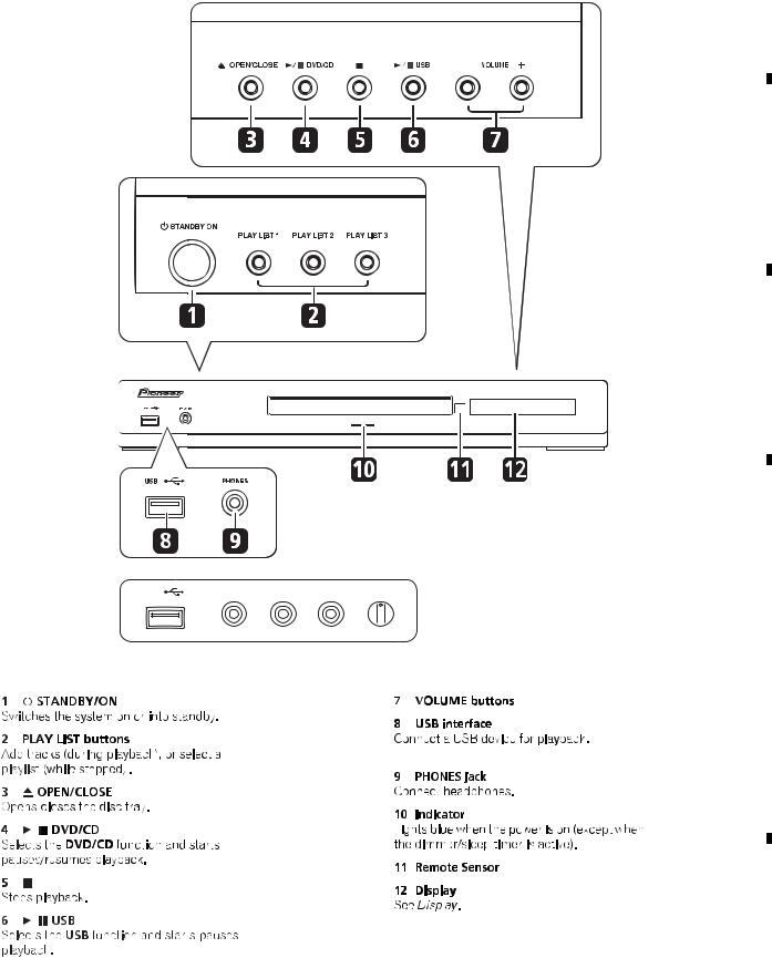
2.2 PANEL FACILITIES
Front panel
A
B
C
XV-DV363
XV-DV365K
D
|
|
|
MIC |
|
USB |
PHONES |
SUB MIC MAIN |
MIN VOL MAX |
|
|
|
|
|
|
|
|
|
|
|
E
F
|
|
|
|
|
|
|
|
7 |
|
|
|
|
|
|
XV-DV363 |
|
|
||||
|
|
|
|
|
|
|
|
|||
|
5 |
|
6 |
|
|
|
7 |
|
8 |
|
|
|
|
|
|
|
|
||||

|
1 |
|
2 |
|
3 |
|
4 |
|
|
|
|
|
|
A Display
B
C
D
E
F
8 |
|
|
|
|
|
|
|
|
|
|
|
|
XV-DV363 |
|
|
|
|
||||
|
1 |
|
2 |
|
|
|
3 |
|
4 |
|
|
|
|
|
|
|
|
||||
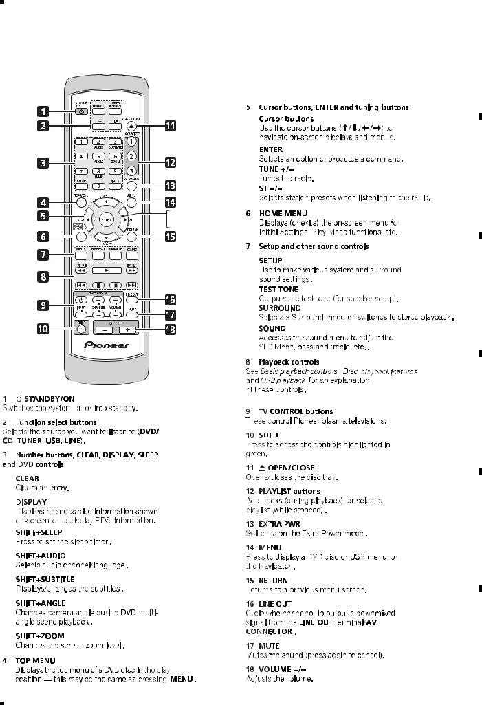
5
Remote control
ECHO
KARAOKE
5
|
6 |
|
7 |
|
8 |
|
|
|
|
|
A
B
(XV-DV356K)
SHIFT+KARAOKE
SHIFT+ECHO
SHIFT+  SHIFT+
C
D
E
F
|
|
|
|
|
|
9 |
|
|
|
|
XV-DV363 |
|
|
||||
|
|
|
|
|
|
|||
|
6 |
|
|
|
7 |
|
8 |
|
|
|
|
|
|
|
|||

|
1 |
|
2 |
|
3 |
|
4 |
|
|
|
|
|
|
3. BASIC ITEMS FOR SERVICE
3.1 CHECK POINTS AFTER SERVICING
A
Check points after servicing (HTZ and system audio)
To keep the product quality after servicing, confirm recommended check points shown below.
|
|
No. |
Procedures |
Check points |
|
|
1 |
Confirm the firmware version on Service Mode. |
The version of the firmware must be latest. |
|
|
Update firmware to the latest one, if it is not the latest. |
||
|
|
|
|
|
|
|
|
|
|
|
|
|
Confirm whether the customer complain has been solved. If the |
The customer complain must not be reappeared. |
|
|
2 |
customer complain occurs with the specific disc, use it for the |
|
|
|
Video, audio and operations must be normal. |
||
|
|
|
operation check. |
|
|
|
|
|
|
|
|
|
|
|
|
|
|
Confirm playback error rates at the innermost and outermost |
The error rates must be less than 5.0e-4. |
|
|
3 |
tracks by using the following disc. |
|
B |
|
|
||
|
|
DVD test disc (GGV1025) |
|
|
|
|
|
|
|
|
|
|
|
|
|
|
4 |
Play back a CD. (track search) |
Audio and operations must be normal. |
|
|
|
|
|
|
|
5 |
Play back a DVD. |
Video, audio and operations must be normal. |
|
|
(Menu operation, Title/chapter search) |
||
|
|
|
|
|
|
|
|
|
|
|
|
6 |
Check the tuner (AM and FM) operations. |
Audio and operations must be normal. |
|
||||
|
|
|
|
|
|
|
7 |
Check the sound from headphone output. |
Sound must be normal, without noise. |
|
|
|
|
|
|
|
8 |
Check the appearance of the product. |
No scratches or dirt on its appearance after receiving it for |
|
|
service. |
||
|
|
|
|
|
|
|
|
|
|
C
See the table below for the items to be checked regarding video and audio:
|
|
Item to be checked regarding video |
Item to be checked regarding audio |
|
|
Block noise |
Distortion |
|
|
|
|
|
|
Horizontal noise |
Noise |
|
|
Dot noise |
Volume too low |
|
|
|
|
|
|
Disturbed image (video jumpiness) |
Volume too high |
|
|
|
|
|
|
Too dark |
Volume fluctuating |
|
|
|
|
|
|
Too bright |
Sound interrupted |
|
|
|
|
D |
|
Mottled color |
|
|
|
|
|
|
|
|
|
|
|
|
|
E
F
10 |
|
|
|
|
|
|
|
|
|
|
|
|
XV-DV363 |
|
|
|
|
||||
|
1 |
|
2 |
|
|
|
3 |
|
4 |
|
|
|
|
|
|
|
|
||||
5 |
6 |
|
7 |
8 |
|
3.2 PCB LOCATIONS |
|
|
|
|
|
|
J |
C |
I |
|
|
|
POWER SUPPLY Unit |
DAMP Assy |
EUROSCART Assy |
|
|
|
|
|
|
FM/AM TUNER Unit |
A |
|
|
|
|
|
|
|
|
|
|
B |
|
|
|
|
|
DVD MAIN Assy |
|
06 LOADER Assy
B
|
E |
|
H |
|
|
|
|
|
D |
|
|
|
|
|
|
||||||||
|
|||||||||||
USB Assy |
MIC Assy |
|
|
|
DISPLAY Assy |
|
|||||
|
(XV-DV365K only) |
|
|
|
|
|
|
|
|||
|
|
|
|
|
|
|
|
|
|
|
|
|
|
|
|
|
|
A |
|
||||
|
|
|
|
|
LOAB Assy |
|
|||||
C
 Bottom view
 Front panel section
D
 Rear view
G |
|
F |
|
|
KEY Assy |
LED Assy |
|
||
|
|
|
|
|
|
|
|
|
|
Mark No. |
Description |
Part No. |
||||
|
|
|
|
|
||
|
LIST OF ASSEMBLIES |
|
||||
|
NSP |
1..06 LOADER ASSY |
VWT1226 |
|||
|
|
2..LOAB ASSY |
VWG2346 |
|||
|
|
1..DAMP ASSY |
XWK3318 |
|||
|
|
1..DVD MAIN ASSY (XV-DV363) |
XWM3341 |
|||
|
|
1..DVD MAIN ASSY (XV-DV365K) |
XWM3342 |
|||
|
NSP |
1..COMPLEX ASSY |
XWM3372 |
|||
|
|
2..DISPLAY ASSY |
XWZ4256 |
|||
|
|
2..USB ASSY |
XWZ4259 |
|||
|
|
2..KEY ASSY |
XWZ4261 |
|||
|
|
2..LED ASSY |
XWZ4263 |
|||
|
NSP |
1..JACK ASSY |
AWM8034 |
|||
|
|
2..EUROSCART ASSY |
AWU8291 |
|||
|
|
|
5 |
|
|
6 |
|
|
|
|
|||
|
|
|
|
|||
Mark No. |
Description |
Part No. |
|
||
|
|
|
|
|
|
|
1..MIC ASSY (XV-DV365K ONLY) |
XWM3375 |
E |
||
|
|
|
|
|
|
> 1..POWER SUPPLY UNIT |
XWR3012 |
|
|||
|
1..FM/AM TUNER UNIT |
AXX7248 |
|
||
|
|
|
|
|
|
|
|
|
|
|
|
F
|
|
|
|
11 |
|
|
XV-DV363 |
|
|
||||
|
|
|
|
|||
|
|
|
7 |
|
8 |
|
|
|
|
|
|
||

|
|
1 |
|
|
2 |
|
|
3 |
|
|
4 |
|
|
|||
|
|
|
|
|
|
|||||||||||
|
|
3.3 JIGS LIST |
|
|
|
|
|
|
|
|
|
|||||
|
|
|
|
Jigs list |
|
|
|
|
|
|
|
|
|
|||
|
|
|
|
|
|
|
|
|
|
|
|
|
||||
|
|
|
|
|
|
|
|
|
|
|
|
|
||||
A |
|
|
|
|
|
|
|
|
|
|||||||
|
|
|
|
|
Name |
Jig No. |
|
|
Remarks |
|
|
|
||||
|
|
|
Service Remote Control Unit |
GGF1381 |
adjustment, diagnosis |
|
|
|
||||||||
|
|
|
|
|
|
|
|
|
|
|
||||||
|
|
|
DVD Test Disc (DVD-Video) |
GGV1025 |
Check of DVD-Video |
|
|
|
||||||||
|
|
|
|
|
|
|
|
|
|
|
||||||
|
|
|
CD Test Disc |
STD-905 |
Check of CD |
|
|
|
||||||||
|
|
|
DVD Data Disc |
GGV1269 |
ID data setting |
|
|
|
||||||||
|
|
|
|
|
||||||||||||
|
|
|
|
|
|
|
|
|
|
|||||||
|
|
|
Speaker Cable with terminal |
SDS1174 (FL/WHITE) |
For checking audio at the SP terminal |
|
|
|||||||||
|
|
|
|
|
|
|
|
SDS1175 (FR/RED), SDS1176 (SL/BLUE) |
|
|
|
|
|
|
||
|
|
|
|
|
|
|
|
SDS1177 (SR/GRAY), SDS1178 (C/GREEN) |
|
|
|
|
|
|
||
|
|
|
|
|
|
|
|
|
|
|
|
|
||||
B |
|
|
|
|
|
|
|
|
|
|||||||
|
|
|
|
Lubricants and Glues list |
|
|
|
|
|
|
|
|
|
|||
|
|
|
|
|
|
|
|
|
|
|
|
|
||||
|
|
|
|
|
|
|
|
|
|
|
|
|
||||
|
|
|
|
|
|
|
|
|
|
|
|
|
||||
|
|
|
|
|
|
|
|
|
|
|
|
|
|
|
|
|
|
|
|
|
|
|
|
|
|
|
|
|
|
|
|
|
|
|
|
|
|
|
Name |
Lubricants and Glues No. |
|
|
Remarks |
|
|
|
||||
|
|
|
Lubricating Oil |
GYA1001 |
refer to "9.3 06 LOADER ASSY" |
|
|
|
||||||||
|
|
|
|
|
||||||||||||
|
|
|
Daifree |
GEM1036 |
refer to "9.3 06 LOADER ASSY" |
|
|
|
||||||||
|
|
|
Silicone Adhesive |
GEM1037 |
refer to "9.4 TRAVERSE MECHANISM ASSY-S" |
|
|
|||||||||
|
|
|
|
|
|
|
|
|
|
|||||||
|
|
|
Screw tight |
GYL1001 |
refer to "8.1.5 MECHANISM ADJUSTMENT" |
|
|
|||||||||
|
|
|
|
|
|
|
|
|
|
|
|
|
||||
C |
|
|
|
|
|
|
|
|
|
|||||||
|
|
|
|
|
|
|
|
|
|
|
|
|
|
|
|
|
|
|
|
|
|
|
|
|
|
|
|
|
|
|
|
|
|
3.4 CLEANING
D
 CLEANING
Before shipping out the product, be sure to clean the following positions by using the prescribed cleaning tools:
|
|
Position to be cleaned |
Cleaning tools |
|
|
|
|
|
|
Pickup leneses |
Cleaning liquid : GEM1004 |
E |
|
Cleaning paper : GED-008 |
|
|
|
||
|
|
|
|
|
|
|
|
F
12 |
|
|
|
|
|
|
|
|
|
|
|
|
XV-DV363 |
|
|
|
|
||||
|
1 |
|
2 |
|
|
|
3 |
|
4 |
|
|
|
|
|
|
|
|
||||

|
5 |
|
6 |
|
7 |
|
8 |
|
|
|
|
|
|
A
B
C
D
E
F
|
|
|
|
|
|
|
|
13 |
|
|
|
|
|
|
XV-DV363 |
|
|
||||
|
|
|
|
|
|
|
|
|||
|
5 |
|
6 |
|
|
|
7 |
|
8 |
|
|
|
|
|
|
|
|
||||

A
B
C
D
E
F
1 |
|
2 |
|
3 |
|
4 |
|
|
|
|
|
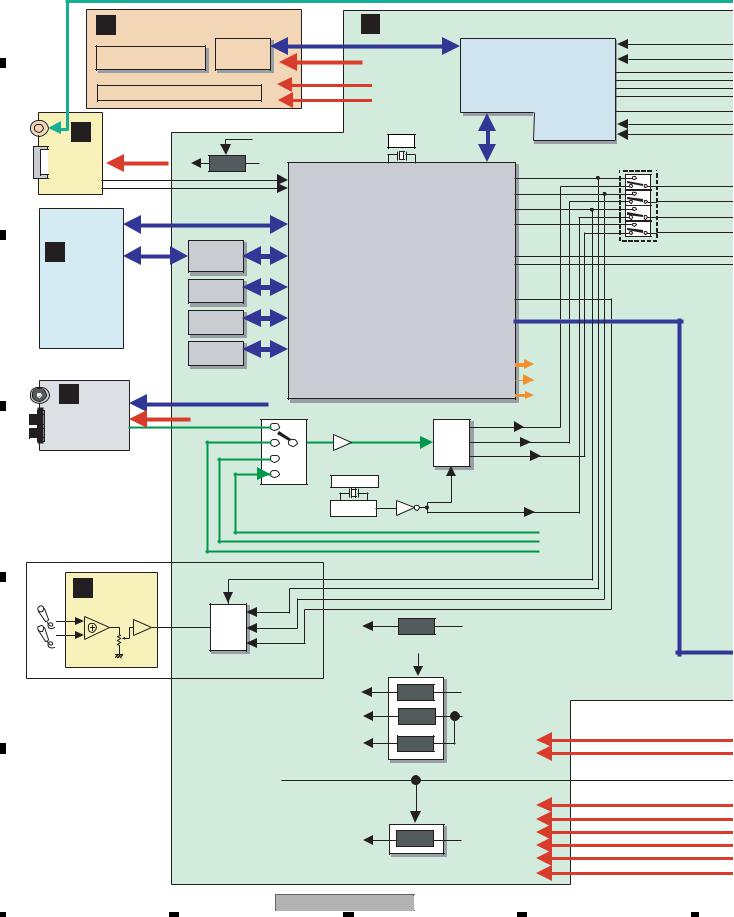
4. BLOCK DIAGRAM
4.1 OVERALL WIRING CONNECTION DIAGRAM and LOAB ASSY
K FM/AMTUNER UNIT (AXX7248)
|
No schematic Diagram |
DI |
|
CN5701 |
B ( B1/5- B 5/5) |
|
|
|
|
|
2 |
DI |
|
||
|
|
CN1 |
|
CKS3376- |
|
|
DVD MAIN ASSY |
|
|
CE |
|
1 |
CE |
|
|
FM |
|
CLK |
|
3 |
CLK |
(XWM3341:XV-DV363/WYXJ5) |
|
|
|
DO |
|
5 |
DO |
||
|
|
|
4 |
|
|
||
|
|
GND |
11P FFC |
|
GND |
|
|
AM |
|
TXL |
(ADD7543) |
6 |
TXL |
(XWM3342:XV-DV365K/WXJ/RE5) |
|
|
|
|
|
||||
|
|
TXR |
|
8 |
TXR |
||
|
|
+9V |
|
7 |
+9V |
|
|
|
|
VSM |
|
9 |
VSM |
|
|
|
|
RDS |
|
10 |
RDS |
|
|
|
|
GND |
|
11 |
GND |
|
|
DVD LOADER |
VWT1226- |
|
|
|
|
|
|
|
|
|
|
|
|
CN101 |
|
CN1 |
|
|
|
|
CN102 |
||
|
|
|
|
|
|
|
|
|
|
|
|
|
|
|
|
|
VKN1243 |
||||
7 |
|
H |
|
|
|
CN3921 |
|
CN5702 |
VKN2045 |
|
OKN8001 |
|
INSIDE |
|
|
12 |
INSIDE |
||||
|
|
|
|
|
|
|
|
|
|
|
|
|
|
|
|||||||
6 |
|
MIC ASSYMIC SW |
1 |
|
|
1 |
MIC SW |
GNDD |
2 |
|
GNDD |
|
W |
|
|
11 |
W |
||||
4 |
|
|
|
F |
|
F |
|
|
|
||||||||||||
2 |
|
|
|
|
|
|
|
|
CKS3370 |
|
|
1 |
|
|
|
|
|
||||
3 |
JA3921 |
|
|
|
|
|
|
-) |
|
|
|
|
|
|
|
V |
|
|
10 |
V |
|
5 |
|
|
|
|
2 |
FFC5P |
|
|
|
|
|
|
MOTORSPINDLE |
|
FFC12P |
||||||
|
AKN7003 |
|
|
|
ECHOCONT |
(XDD3232 |
2 |
ECHOCONT |
VS(VREF) |
3 |
|
VS(VREF) |
|
|
|
|
|||||
1 |
|
(XWM3375: |
|
|
V+10V |
3 |
|
|
3 |
V+10V |
|
|
U |
|
|
9 |
U |
||||
|
|
|
|
|
|
|
|
|
|
|
|||||||||||
2 |
JA3922 |
|
|
GND |
5 |
|
|
5 |
GND |
VCC |
|
|
VCC |
DXB1860- |
HB |
|
|
8 |
HB |
||
1 |
|
|
|
|
|
MIC |
4 |
|
|
4 |
MIC |
4 |
|
TRAVERSE MECHA ASSY |
|
|
|
|
|
||
|
|
|
|
|
|
|
|
|
|
|
|
|
|
|
|
|
|
|
|||
3 |
RKN1004 |
XV-DV365K/WXJ/RE5) |
|
|
|
|
|
E |
5 |
|
E |
|
W- |
|
|
7 |
W- |
||||
|
|
|
|
|
|
|
|
|
|
|
|||||||||||
|
|
|
|
|
|
D |
6 |
|
D |
|
|
|
|||||||||
|
|
|
|
|
|
|
|
|
|
|
|
|
|
|
|
|
W+ |
|
|
6 |
W+ |
|
|
|
|
|
|
|
|
|
|
|
|
C |
7 |
|
C |
|
V- |
|
|
5 |
V- |
|
|
|
|
|
|
|
|
|
|
|
|
|
|
|
|
|
|
||||
|
|
J |
|
|
|
|
|
|
|
|
|
SW(DVD/CD) |
8 |
|
SW(DVD/CD) |
|
V+ |
|
|
4 |
V+ |
|
|
|
|
|
|
|
|
|
|
|
|
) |
|
|
|
|
|||||
|
|
|
|
CN3 |
|
|
CN1001 |
B |
10 |
- |
B |
|
U+ |
|
|
2 |
U+ |
||||
|
|
|
|
|
|
(ADD7545 |
|
|
|
||||||||||||
|
|
|
|
|
|
|
|
|
|
|
|
RF |
9 |
|
RF |
|
U- |
|
|
3 |
U- |
|
|
|
|
|
|
|
|
|
|
|
|
|
|
|
|
|
|
||||
|
|
POWER |
|
AC_DET |
1 |
PG13KK-F22 |
|
1 |
AC_DET |
VR650 |
12 |
|
VR650 |
|
|
|
|
|
|
||
|
|
|
|
|
B13B-PH-K-S |
|
|
B13B-PH-K-S |
|
A |
11 |
24PFFC |
A |
|
V+5S |
|
|
1 |
V+5S |
||
|
|
SUPPLY UNIT |
|
SW10.5V |
2 |
|
|
|
2 |
SW10.5V |
VRCOM |
13 |
VRCOM |
|
|
|
|
|
|
||
|
|
(XWR3012) |
|
EV5.0V |
3 |
|
|
|
3 |
EV5.0V |
VR780 |
14 |
|
VR780 |
|
|
|
|
CN103 |
||
|
|
|
SW5.0V |
4 |
|
|
|
4 |
SW5.0V |
GNDD |
15 |
|
GNDD |
STEPPINGMOTOR |
|
|
|
VKN1235 |
|||
|
|
2 LIVE |
|
|
SW3.3V(B) |
7 |
|
|
|
7 |
SW3.3V(B) |
|
|
|
|
ST1-(~A~) |
|
FFC4P |
4 |
ST1-(~A~) |
|
|
|
|
|
|
|
|
|
|
|
|
|
LD(780) |
|
|
LD(780) |
|
ST2-(~B~) |
|
|
1 |
ST2-(~B~) |
|
|
|
|
|
SW6.8V |
5 |
|
|
|
5 |
SW6.8V |
16 |
|
|
ST2+(B) |
|
|
2 |
ST2+(B) |
||
|
|
CN1 |
|
|
GND |
6 |
|
|
|
6 |
GND |
PD |
17 |
|
PD |
|
ST1+(A) |
|
|
3 |
ST1+(A) |
|
|
|
|
|
|
|
|
|
|
|
|
LD(650) |
18 |
|
LD(650) |
|
|
|
|
|
|
|
|
1 NEUTRAL |
|
|
SW3.3V(A) |
8 |
|
|
|
8 |
SW3.3V(A) |
GNDD |
19 |
|
GNDD |
|
|
|
|
|
|
|
|
|
|
|
Pwr-ctr |
9 |
|
|
|
9 |
Pwr-ctr |
VSHF |
20 |
|
VSHF |
|
|
|
|
|
|
|
|
|
|
|
|
|
|
|
|
|
|
|
|
|
|
|
|||||
AC POWER CORD |
|
|
|
GND |
10 |
|
|
|
10 |
GND |
TRKG DRV |
21 |
|
TRKG DRV |
CN602 |
CN601 |
|
CN104 |
|||
|
|
|
|
|
|
|
|
TRKG RTN |
|
|
TRKG RTN |
|
|||||||||
|
|
|
|
|
FL DC- |
11 |
|
|
|
11 |
FL DC- |
|
22 |
|
|
2 |
S5B-PH-K-S |
|
B5B-PH-K-S |
||
|
|
|
|
|
|
|
|
|
|
|
|
|
|||||||||
|
|
|
|
|
FL DC+ |
12 |
|
|
|
12 |
FL DC+ |
FOCS DRV |
23 |
|
FOCS DRV |
1 |
LOAD- |
1 |
|
1 |
LOAD- |
|
|
|
|
|
|
|
|
|
|
|
|
|
|||||||||
|
|
|
|
|
|
|
|
FOCS RTN |
|
|
FOCS RTN |
LOAD+ |
|
|
|
|
|||||
|
|
|
|
|
-25.5V |
13 |
|
|
|
13 |
-25.5V |
24 |
|
|
2 |
|
2 |
LOAD+ |
|||
|
|
|
|
|
|
|
|
|
|
|
|
SW2 |
|
||||||||
|
|
|
|
|
|
|
|
|
|
|
|
|
|
|
|
|
3 |
|
3 |
SW2 |
|
|
|
|
|
|
|
|
|
|
|
|
|
|
|
|
|
|
|
|
|||
|
|
|
|
|
|
|
|
|
|
|
|
|
|
|
PICK UP ASSY |
A |
GNDD |
4 |
|
4 |
GNDD |
|
|
|
|
+B |
GND |
|
|
|
|
|
|
|
|
|
|
5 |
|
5 |
SW1 |
||
|
|
|
CN2 -B2PVH |
|
|
|
|
|
|
|
|
|
OWY8087- |
SW1 |
|
||||||
|
|
|
2 |
1 |
|
|
|
|
|
|
|
|
|
|
|
|
|
|
|||
|
|
|
|
|
|
|
|
|
|
|
|
|
|
|
|
|
|
PF05PP-B40 |
|
|
|
|
|
|
|
|
|
|
|
|
|
|
|
|
|
|
|
LOAB ASSY |
|
|
|
||
|
|
|
|
|
|
|
|
|
|
|
|
|
|
|
|
(VWG2346) |
|
|
|
|
|
|
|
|
|
|
|
|
|
|
|
|
|
|
|
|
|
ADX7480- |
|
|
|
|
|
14 |
|
|
|
|
|
|
|
|
|
|
|
XV-DV363 |
|
|
|
|
|
|
|
|
|
|
|
1 |
|
|
|
|
|
|
2 |
|
|
|
|
|
3 |
|
|
4 |
|
|
|

|
5 |
|
6 |
|
|
|
|
CN931 AKP7210- (AKP7211) |
DATA2+ SHIELDDATA2 |
DATA2DATA1+ |
SHIELDDATA1 |
HDMI OUTPUT |
CLOCK- |
CEC |
NC |
HDMISCL HDMISDA |
GNDDDC/CEC |
+5V |
DETECTPLUGHOT |
||||
DATA1- |
DATA0+ |
SHIELDDATA0 DATA0- |
CLOCK+ |
SHIELDCLOCK |
|||||||||||
|
2 |
4 |
|
6 |
|
8 |
10 |
|
12 |
|
14 |
16 |
|
18 |
|
|
1 |
3 |
5 |
|
7 |
9 |
|
11 |
|
13 |
|
15 |
17 |
|
19 |
7
VSEL1 |
|
1 |
|
SQEEZE |
2 |
|
|
V+10 |
|
3 |
|
TVOUT_R |
4 |
|
|
GND |
|
5 |
|
TVOUT_L |
6 |
|
|
TVMUTE |
|
7 |
|
SCART_R |
8 |
|
(ADD7544) |
GND |
|
9 |
|
SCART_L |
10 |
|
|
V+5 |
|
11 |
|
VSEL2 |
12 |
|
|
B |
|
13 |
FFC |
GND |
14 |
|
|
G |
|
15 |
23P |
GND |
16 |
|
|
|
|
||
R |
|
17 |
|
DVDPOWER |
18 |
|
|
S_C |
|
19 |
|
GND |
20 |
|
|
V |
|
21 |
|
GND |
22 |
|
|
S_Y |
|
23 |
|
CN451
CKS3388-
8
A
1 |
VSEL1 |
|
|
JA451 |
|
||
2 |
SQEEZE |
|
|
XKB3054- |
|
||
3 |
V+10 |
|
|
EURO CONNECTOR |
|
||
|
|
|
|
|
|
||
4 |
TVOUT_R |
|
|
1 |
|
R OUT |
|
5 |
GND |
|
|
|
2 |
R IN |
|
6 |
TVOUT_L |
|
|
3 |
|
L OUT |
|
7 |
TVMUTE |
|
|
|
4 |
GND |
|
8 |
SCART_R |
I |
|
5 |
|
GND |
|
9 |
GND |
|
|
6 |
L IN |
|
|
10 |
SCART_L |
|
7 |
|
B |
|
|
11 |
V+5 |
|
|
8 |
SQUEEZE |
|
|
12 |
VSEL2 |
|
|
9 |
|
GND |
|
13 |
B |
EURO SCART |
10 |
NC |
|
||
14 |
GND |
ASSY |
|
11 |
|
G |
|
15 |
G |
|
|
12 |
NC |
|
|
16 |
GND |
(AWU8291) |
13 |
|
GND |
|
|
17 |
R |
|
14 |
GND |
|
||
|
|
|
|
||||
18 |
DVDPOWER |
|
|
15 |
|
R/C |
|
19 |
S_C |
|
|
|
16 |
BLANK |
|
20 |
GND |
|
|
17 |
|
GND |
|
21 |
V |
|
|
|
18 |
GND |
|
22 |
GND |
|
|
19 |
|
V/Y |
|
23 |
S_Y |
|
|
|
20 |
NC |
|
CN461 |
|
|
21 |
|
GND |
B |
|
|
|
|
|
|
|||
CKS3388- |
|
|
|
|
|
||
|
|
|
|
JA403 |
|
|
|
|
|
|
|
XKB3060- |
|
COMPOSITE |
|
|
|
|
(VKB1122) |
|
|
||
VIDEO
V OUTPUT
CN5602 |
CKS3378- |
FLDATA |
FLCK |
FLCS |
REMOCON |
VE+5 |
VFDP |
FLDCFLDC+ |
GNDD |
GNDD KEY1 |
KEY2 KEY2A |
CN5601 |
15p:CKS3380 |
HPMUTE |
HP L |
GNDD |
HP R |
HP DET |
GNDUSB |
V5USB |
V5USB |
USB DP2 |
USB DM2 |
GNDUSB |
KEY2 |
KEY1 |
V+10 |
LED |
|
|
13 |
|
11 |
|
9 |
|
7 |
5 |
3 |
1 |
|
|
1 |
|
3 |
|
5 |
|
7 |
|
9 |
|
11 |
|
13 |
|
15 |
|
|
|
12 |
|
10 |
|
8 |
6 |
|
4 |
2 |
|
|
|
2 |
|
4 |
|
6 |
|
8 |
|
10 |
|
12 |
|
14 |
|
|
|
|
|
|
|
13P FFC(ADD7541) |
|
|
CN5906 |
|
|
|
|
|
|
|
|
15P FFC (XDD3234) |
||||||||||
|
|
|
|
|
|
|
|
|
|
|
|
|
|
|
|
|
|
|
|
|
||||||||
CN5901 |
CKS3378- |
FLDATA |
FLCK |
FLCS |
REMOCON |
VE+5 |
|
|
|
KEY1 |
ASSYKEY2 KEY2A |
KEY ASSY |
HPMUTE |
HPL |
GNDD |
HPR |
DETHP |
GNDUSB |
V5USB |
V5USB |
DP2USB |
DM2USB |
GNDUSB |
KEY2 |
KEY1 |
LED |
V+10 |
|
DISPLAYVFDP FLDCFLDC+ GNDD GNDD |
15p:CKS3380 |
|||||||||||||||||||||||||||
|
|
|
2 |
|
4 |
|
6 |
8 |
|
10 |
12 |
|
|
|
2 |
|
4 |
|
6 |
|
8 |
|
10 |
|
12 |
|
14 |
|
|
|
1 |
|
3 |
|
5 |
|
7 |
9 |
11 |
13 |
G |
|
1 |
|
3 |
|
5 |
|
7 |
|
9 |
|
11 |
|
13 |
|
15 |
|
|
|
|
|
|
|
|
|
|
|
|
|
|
|
|
|
|
|
|
|
|
|
|
|
|
|
|
|
IC5902 |
|
|
D |
|
(XWZ4256) |
(XWZ4261) |
|
|
|
|
|
|
|
|
|
|
|
|
|
|
|
|
||||||
Vcc |
|
|
|
|
|
|
|
|
|
|
|
|
|
|
|
|
|
|
|
|||||||||
|
|
|
|
|
|
|
|
|
|
|
|
|
|
|
|
|
|
|
|
|||||||||
GND |
|
|
|
|
|
|
|
|
|
|
|
|
|
|
|
|
|
|
|
|
|
|
|
|
|
|
|
|
Vout |
|
|
|
|
|
|
|
FL |
|
|
|
|
|
|
|
|
|
|
|
|
|
|
|
|
|
|
|
|
AAV7104(AAV7107)
GP1UM27XKOVF
CN5908 CN5907
CN3001 |
CN3101 |
||
AKP7199- |
AKM7077- |
|
|
PCON |
19 |
19 |
PCON |
XHPSEL |
18 |
18 |
XHPSEL |
HPL |
17 |
17 |
HPL |
GND |
16 |
16 |
GND |
HPR |
15 |
15 |
HPR |
GND |
14 |
14 |
GND |
3.3V |
13 |
13 |
3.3V |
XRST |
12 |
12 |
XRST |
XPDN |
11 |
11 |
XPDN |
XMUTE |
10 |
10 |
XMUTE |
GND |
9 |
9 |
GND |
SDA |
8 |
8 |
SDA |
SCL |
7 |
7 |
SCL |
GND |
6 |
6 |
GND |
XOTW |
5 |
5 |
XOTW |
XSD |
4 |
4 |
XSD |
SROUT |
3 |
3 |
SROUT |
POWER |
2 |
2 |
POWER |
PLCCONT |
1 |
1 |
PLCCONT |
|
|
|
|
CKS3370 |
|
|
|
KEY2A |
1 |
||
|
|
|
GND |
2 |
|
|
|
|
KEY1 |
3 |
|
|
|
|
LED |
4 |
|
|
V+10V |
|
V+10 |
5 |
|
|
GND |
LED |
|
||
|
3 |
2 |
1 |
CN5909 CKS3368 |
|
|
3P FFC |
|
|
|
|
|
(XDD3229-) |
|
343BBT-SLR |
||
|
V+10V |
LED |
GND CN5603 CKS3368 |
||
|
1 |
2 |
3 |
|
|
F |
LED ASSY |
|
|
|
|
(XWZ4263) |
|
|
|||
GA UPPER |
|
|
|
||
EU,RUSSIA,KUC & J
5P FFC (XDD3231)
CKS3370
1KEY2A
2GND
3KEY1
4LED
5V+10
E USB ASSY (XWZ4259)
CN3002 |
CN3102 |
|
|
|
|
|
|
||
AKP7199- |
AKM7077- |
|
|
|
|
|
|
|
|
SDATA1 |
19 |
19 |
SDATA1 |
|
|
|
|
|
|
SDATA2 |
18 |
18 |
SDATA2 |
|
|
|
|
|
|
SDATA3 |
17 |
17 |
SDATA3 |
|
|
|
|
|
|
GND |
16 |
16 |
GND |
|
|
|
|
|
|
MCLK |
15 |
15 |
MCLK |
|
|
|
|
|
|
GND |
14 |
14 |
GND |
|
|
|
|
C ( C1/2- C 2/2)DAMP ASSY |
|
GND |
11 |
11 |
GND |
|
|
|
|
||
SCLK |
13 |
13 |
SCLK |
|
|
|
|
|
|
LRCLK |
12 |
12 |
LRCLK |
|
|
|
|
|
|
LIN1_L |
10 |
10 |
LIN1_L |
|
|
|
|
(XWK3318) |
|
LIN1_R |
8 |
8 |
LIN1_R |
|
|
|
|
|
|
GND |
9 |
9 |
GND |
|
|
|
|
|
|
GND |
7 |
7 |
GND |
|
|
|
|
|
|
S_TVOUT_L 6 |
6 |
S_TVOUT_L |
|
|
|
|
|
|
|
GND |
5 |
5 |
GND |
|
|
|
|
|
|
S_TVOUT_R 4 |
4 |
S_TVOUT_R |
|
|
|
|
|
|
|
RECMUTE |
3 |
3 |
RECMUTE |
CN3201 |
1 |
2 |
VH-B2P |
|
|
GND |
2 |
2 |
GND |
|
|
||||
SDATA4 |
1 |
1 |
SDATA4 |
|
|
|
|
RKN1004 |
|
|
|
|
|
|
GND |
|
|
|
|
|
|
|
|
|
+B |
|
|
|
|
|
|
|
|
|
|
|
|
SR OUT |
|
|
|
|
|
|
|
|
|
|
XV-DV363 |
|
|
5 |
|
|
|
|
|
6 |
7 |
C
D
JA5902
AKN7003-
HP OUT
HEAD PHONE
JA602
USB |
XKP3086 |
|
TVIN_L |
|
|
TVIN_R |
AUDIO |
|
|
|
|
LINEOUT_L |
IN/OUT |
|
|
|
E |
LINEOUT_R
CN3111
AKB7114
CN3211
AKE7121
1FR+
2FR-
3RR+
4 RR-
5FL+
6FL-
6ch SP OUT
7RL+
8RL-
9C+
10C-
11SW+
12 |
SW- |
F |
15
8
|
1 |
|
2 |
|
3 |
|
4 |
|
|
|
|
|
|
4.2 OVERALL BLOCK DIAGRAM
A |
|
|
|
|
|
|
|
|
|
D DISPLAY ASSY |
|
B DVD MAIN ASSY |
|
PCON (from SMPS or D-AM |
|
|
|
|
|
|
|
|
|
|
|
FL |
Display |
|
|
DC DET |
|
|
|
Driver |
|
VE+5 |
|
||
|
|
|
SYSTEM |
|
|||
|
|
|
|
|
SCL |
||
|
|
|
|
|
|
||
|
|
|
|
FL DC+/- |
|
UCOM |
SDA |
|
|
|
KEY |
|
|
|
MUTE |
|
|
|
VFDP |
|
|
RESET |
|
|
|
|
|
|
|
|
PDN |
|
|
E |
|
|
|
|
SD |
|
HP |
|
|
|
|
OTW |
|
B |
|
USB POWER |
27M |
|
|
||
USB |
V+5USB |
|
|
|
|
||
|
|
|
|
|
|||
|
ASSY |
5V |
V+6R8 |
|
ACLK |
|
|
|
|
|
USB DP |
|
BE |
BCKO |
|
|
USB |
|
USB DM |
|
ALRCK |
||
|
|
|
|
||||
|
|
|
|
|
|
LRCKO |
|
|
|
|
|
|
|
MCLK |
|
|
|
|
|
|
MT1389 |
MCKO |
|
|
|
|
|
|
|
||
|
|
|
|
|
|
ASDAT0 |
|
|
|
|
|
|
|
DATAO |
|
|
A |
|
|
|
|
|
|
|
|
MOTOR |
|
|
ASDAT1 |
|
|
|
|
|
|
|
|
||
|
|
|
DRIVER |
|
|
ASDAT2 |
|
|
LOAB ASSY |
64M |
|
|
|
|
|
|
|
|
|
|
• AUDIO PROCESSING |
|
|
MCDATA |
|||
|
|
SDRAM |
|
|
|
||||
|
|
|
• Audio Decode |
|
|
|
|||
|
|
|
|
|
|
|
|
||
C |
LOADER |
|
16M |
|
• Bass Management |
|
|
|
|
MECHA |
FLASH |
|
• Virtual Surround |
|
|
|
|||
|
|
|
|
|
|||||
|
|
|
|
• Preset EQ |
|
|
|
|
|
|
|
|
64k |
|
|
|
|
|
|
|
|
|
|
|
|
|
|
|
|
|
|
EEPROM |
|
etc. |
|
|
G,B,R |
||
|
|
|
|
|
|
|
|||
|
K |
|
|
|
|
|
|
|
V |
|
|
|
|
|
|
|
Y,C |
||
|
|
|
|
|
|
|
|
||
|
FM/AM |
+9V |
TUNER |
|
|
|
|
ADBCK |
|
|
TUNER |
|
|
|
|
||||
|
|
SCART |
|
|
|
|
ADLRCK |
||
|
UNIT |
|
|
|
A/D |
|
|||
|
|
LINE/TV |
|
|
AK5358AET |
ADDATA |
|||
|
|
|
|
|
|||||
|
|
|
|
|
|
|
|||
|
|
|
|
|
|
|
|
|
|
|
|
|
MCACC |
|
|
|
|
|
|
|
|
|
|
|
12.288M |
ADMCK0 |
|
||
D |
|
|
|
|
|
|
|||
|
|
|
|
|
|
|
|
|
|
|
|
|
|
|
74HCU04 |
|
|
ADMCK1 |
|
|
|
|
|
|
|
|
|
|
MCACC |
|
XV-DV365K/WXJ/RE55 |
|
|
|
|
|
|
|
LINE |
|
ONLY |
|
|
|
|
|
|
|
SCART |
|
|
|
|
|
|
|
|
|
|
|
H |
|
MCLK |
|
|
|
|
|
|
|
|
|
|
|
|
|
|
|
|
|
MIC ASSY |
|
|
ACLK |
|
|
|
|
|
|
|
|
A/D |
ALRCK |
+9V |
9V |
SW+10.5V |
||
|
|
|
AK5358AET |
MCDATA |
|||||
|
|
|
|
|
DVD POWER |
|
|
|
|
|
|
|
|
|
|
|
|
|
|
E |
|
|
|
|
|
|
|
|
|
|
|
|
|
|
V+5V |
SW |
SW5.0V |
|
|
|
|
|
|
|
V+3 |
SW |
SW3.3V(A) |
||
|
|
|
|
|
V+1R8 |
1.8V |
|
|
|
|
|
|
|
PWRCONT |
|
|
|
|
|
|
|
|
|
|
|
|
|
|
V+10 |
|
|
|
|
|
|
|
|
|
VE+5 |
F |
|
|
|
|
V+5 |
SW |
VE+5 |
|
|
|
|
|
|
|
V+6R8 |
||||
|
|
|
|
|
|
|
|
|
|
|
|
|
|
|
|
|
|
|
V+3R3 |
|
16 |
|
|
|
XV-DV363 |
|
|
|
|
|
1 |
|
|
2 |
|
3 |
|
|
4 |

|
5 |
|
6 |
|
7 |
|
8 |
|
|
|
|
|
|
A
PCON (from SMPS or D-AMP)
DC DET
SCL
SDA
MUTE
RESET
PDN
SD
OTW
FRONT L
C DAMP ASSY
|
|
HP AMP |
FRONT R |
|
MODULATER |
|
|
|
|
TAS5508BPAG |
HP SEL |
|
CENTER |
|
|
PWMA P |
DRIVER |
SUB WOOFER |
|
|
TAS5122DCA |
|
||
|
PWMA M |
|
||
|
|
|
||
|
|
|
|
|
|
RESET |
|
REAR L |
B |
|
SD |
|
|
|
|
|
|
|
|
|
PWMB P |
|
REAR R |
|
|
|
|
|
|
|
PWMB M |
|
|
|
|
ch7 ch8 PWM |
LINE OUT |
|
|
|
|
|
||
|
LPF |
|
LINE IN |
|
|
|
|
|
|
|
|
|
SR OUT |
|
+3.3V |
|
|
|
|
LINE |
|
|
|
C |
|
|
|
|
|
SCART |
|
|
|
|
MCACC |
|
|
MCACC MIC |
|
|
|
|
SCART (EU) |
|
|
G, B, R |
|
|
|
|
Y, C |
Scart |
|
|
|
|
|
|
|
|
|
Circuit |
I |
|
|
V |
|
D |
|
|
|
|
||
|
|
|
EUROSCART |
|
G, B, R |
|
|
ASSY |
|
V |
Video |
V |
|
|
AMP |
Composite |
|||
Y, C |
Y, C |
|||
|
|
HDMI |
TX |
|
|
|
|
|
HDMI OUT |
||||
|
|||||
Transmitter |
|
|
|
||
|
|
|
E |
||
|
|
|
|
||
V+3
V+1R8
FLDC +/-
+B
VFDP
|
|
|
|
|
|
|
SW10.5V |
|
|
|
|
|
|
|
|
|
|
|
|
|
|
|
|
|
|
|
|
|
|
|
|
|
|
|
|
|
|
|
|
|
|
|
|
|
FV5.0V |
|
|
|
|
|
|
|
|
|
|
|
|
|
|
|
|
|
|
|
|
|
|
|
|
|
|
|
|
|
|
|
|
|
|
|
|
|
SW 5.0V |
|
|
|
|
|
|
|
|
|
F |
|
|
|
|
|
|
|
|
|
|
|
|
|
|
|
|
|
|||
|
|
|
|
|
|
|
|
|
|
|
|
|
|
|
|
|
||
|
|
|
|
|
|
|
|
|
|
J |
|
|
|
|
|
|
||
|
|
|
|
|
|
|
SW 6.8V |
|
|
POWER SUPPLY UNIT |
|
AC IN |
||||||
|
|
|
|
|
|
|
|
|
|
|||||||||
|
|
|
|
|
|
|
SW |
|
|
|
|
|
|
|||||
|
|
|
|
|
|
|
|
|
|
|
|
|
|
|
|
|
|
|
|
|
|
|
|
|
|
SW |
|
|
|
|
|
|
|
17 |
|
|
|
|
|
|
|
|
|
|
|
|
|
|
|
|
|
|
|
|||
|
|
|
|
|
|
|
|
|
|
|
|
|
|
|
|
|
||
|
|
|
|
|
|
|
|
|
|
|
|
|
|
|
|
|
||
|
|
|
|
|
|
|
|
|
|
|
XV-DV363 |
|
||||||
|
|
|
|
|
|
|
|
|
|
|
|
|
|
|
|
|||
|
|
5 |
|
|
6 |
|
|
|
7 |
|
8 |
|
|
|||||
|
|
|
|
|
|
|
|
|
||||||||||
|
1 |
|
2 |
|
3 |
|
4 |
|
|
|
|
|
|
5. DIAGNOSIS
5.1 METHOD FOR DIAGNOSING DEGRADATION OF THE LDS ON THE PICKUP
A
Case when this diagnosis is required :
When playback of any disc, including a test disc (DVD: GGV1025, CD: STD-905), won't play or doesn't play
 How to diagnose
In the case mentioned above, degradation of the laser diodes (LDs) mounted on the 06SD Pickup Assy-S is suspected. Measure the voltage between the two ends of one of the resistors mentioned below.
 No playback of a DVD :
B
Measure the voltage between the both ends of R322 or R325 on the DVD MAIN Assy. If the voltage is 0.4 V or higher, the 650-nm LD is degraded.
 No playback of a CD :
Measure the voltage between the both ends of R321 or R326 on the DVD MAIN Assy. If the voltage is 0.4 V or higher, the 780-nm LD is degraded.
If the measurements show degradation of an LD, replace the 06SD Pickup Assy-S.
C |
|
|
|
|
|
|
|
|
|
|
|
|
|
|
|
|
|
|
|
|
|
|
|
|
|
|
D |
PICKUP ASSY |
|
|
|
|
|
|
|
|
|
|
|
|
|
B DVD MAIN ASSY |
|
||||||||||
|
|
|
|
CN101 |
|
|
|
|
|
|
|
|
|
|
|
|
|
|
|
|
|
|||||
|
11 1 1 |
R315 XWM 00 0 0 |
|
|
|
|
|
|
|
|
|
|
|
|
|
ICT |
|
FC1 |
|
|
|
|||||
|
|
|
R372 |
R375 |
|
|
C374 |
|
|
|
|
R325 Q307 |
|
R1001 |
|
|
|
|||||||||
|
|
|
|
|
|
|
|
|
|
|
|
|
|
|
|
|||||||||||
|
R318 |
|
|
|
|
|
|
|
|
|
|
|
|
|
B1 |
|
|
|||||||||
|
1 |
|
5 |
Q305 |
|
|
|
|
L308 |
|
|
|
|
|
||||||||||||
|
|
|
|
|
R314 |
|
3 |
|
4 |
|
C371 |
|
C373 |
|
|
|
|
R326 |
R322 C309 |
|
|
|
||||
|
12 |
Q304 |
|
|
|
|
|
|
|
|
|
|
|
|
|
|
|
|
||||||||
|
|
|
|
|
|
|
|
|
|
|
|
|
|
|
|
|
|
|||||||||
E |
|
|
|
|
|
R313 |
|
|
|
|
|
|
L309 |
|
|
|
|
|
|
|
||||||
|
|
CONTACT |
|
|
|
|
|
|
|
|
|
|
|
|
|
|
|
Q308 |
|
|
|
|
|
|||
|
|
|
24 |
|
|
|
|
|
|
|
|
|
2 |
CN101 |
|
|
1 |
|
|
|
|
|
||||
|
|
SIDE |
|
|
|
|
|
|
|
|
|
|
|
|
|
|
C310 |
|
|
|||||||
|
|
|
|
|
|
|
|
|
|
|
|
|
|
|
|
|
R321 |
|
|
|
||||||
|
|
|
|
|
|
|
|
|
|
|
|
|
|
|
|
|
|
|
|
|
|
|||||
|
R134 |
|
23 |
|
|
|
|
|
|
|
|
1 |
|
|
|
|
|
|
|
Front side |
SIDE A |
|
||||
|
|
|
|
|
|
|
|
|
|
|
SIDE |
|
|
|
|
|
|
|||||||||
|
R135 |
|
|
|
|
|
|
|
|
|
|
|
|
|
|
4 |
|
|
|
|
|
|
||||
|
|
|
|
|
|
|
|
|
|
|
|
C372 |
CONTACT |
15 |
|
|
|
[CN5603] |
|
|
|
|||||
|
|
R136 |
C133 |
C161 |
|
R371 |
R373 |
R374 |
|
|
|
C773 |
|
CN5601 |
|
|
|
|
||||||||
|
|
|
|
|
|
R772 |
|
|
|
C320 |
|
|
|
|||||||||||||
|
C144 |
|
|
|
|
|
|
|
|
|
|
|
|
|
|
|||||||||||
|
|
|
|
|
|
|
|
|
C771 |
|
R310 |
|
|
|
||||||||||||
|
|
|
|
C131 |
|
|
3 |
|
1 |
|
|
|
|
|||||||||||||
|
|
|
|
|
|
|
|
|
|
|
|
|||||||||||||||
|
|
|
|
|
|
|
|
|
|
|
|
|
|
|||||||||||||
|
C145 |
|
|
C146 |
23 |
|
|
|
|
|
|
4 |
|
5 |
|
|
|
|
|
|
|
|
|
|||
|
|
|
|
|
|
|
|
|
|
|
|
|
|
|
|
|
|
|
|
|
|
|||||
|
|
|
|
|
|
|
|
|
|
|
|
|
|
|
IC771 |
|
|
|
|
|
|
|
|
|
||
|
|
|
|
|
|
|
|
|
C132 |
|
|
|
|
|
|
R771 |
|
|
|
|
|
|
|
|
||
|
|
|
|
|
|
|
|
|
|
|
|
|
|
|
L772 |
|
|
|
|
|
|
|
|
|||
F |
|
|
|
|
|
|
|
|
|
|
|
|
|
|
|
|
|
|
|
|
|
|
|
|
||
|
|
|
|
|
|
|
|
|
|
|
|
|
|
|
|
|
|
|
|
|
|
|
|
|
|
|
|
|
|
|
|
|
|
|
|
C781 |
|
|
|
|
|
C772 |
|
|
1 |
|
|
|
|
|
|
|
|
|
18 |
|
|
|
|
|
|
|
|
|
|
|
|
|
|
|
|
|
|
|
|
|
XV-DV363 |
|
|
|
|
|
|
|
|
|
1 |
|
|
|
|
|
|
|
|
|
|
|
|
|
2 |
|
|
|
3 |
|
4 |

|
|
5 |
|
6 |
|
|
7 |
|
|
8 |
|
|
|
|
|
||||||
5.2 DVD TROUBLE SHOOTING |
|
|
|
|
||||||
|
|
|
|
|
|
|
||||
|
No. |
Symptoms |
Diagnosis Contents |
|
|
Possible Defective Points |
||||
|
1 |
The power is not turned on. |
Are wires of output connector (POWER SUPPLY Unit) and CN1001 |
Connector / cable |
||||||
|
|
|
|
(DVD MAIN Assy) disconnected or damaged ? |
|
|||||
|
|
|
|
|
|
|
|
|||
|
|
|
|
|
|
|
||||
|
|
|
|
Check that the following voltage is output : |
|
POWER SUPPLY Unit |
||||
|
|
|
|
Q1202-source on the DVD MAIN Assy: 3.3V |
|
|
|
|
||
|
|
|
|
|
||||||
|
2 |
An opening screen is not |
Are the signals output from IC201-pin 97 (MDATA) and pin 98 (SCLK) |
DVD MAIN Assy |
||||||
|
|
displayed on the monitor |
on the DVD MAIN Assy ? (in the range of 0-3V) |
|
DVD IC (IC201) |
|||||
|
|
(The FL display lights. The |
|
|
|
|
|
|
|
|
|
|
mechanism does not work.) |
Are the signals input into IC5501-pin 50 (MDATA) and pin 51 (SCLK) on |
DVD MAIN Assy |
||||||
|
|
|
|
the DVD MAIN Assy ? (in the range of 0-3V) |
|
UCOM (IC5501) |
||||
|
|
|
|
|
|
|
||||
|
|
|
|
Check that the following voltage are output : |
|
DVD MAIN Assy |
||||
|
|
|
|
Q1302-collector on the DVD MAIN Assy: 5V |
|
5V Regulator IC (IC751) |
||||
|
|
|
|
|
|
|
|
|
||
|
|
|
|
Is a resonator (X201: 27MHz) on the DVD MAIN Assy oscillating ? |
DVD MAIN Assy |
|||||
|
|
|
|
Crystal resonator (X201) |
||||||
|
|
|
|
|
|
|
|
DVD IC (IC201) |
||
|
|
|
|
|
|
|
|
|||
|
|
|
|
• Is a signal input into IC203-pin26 (PCE#) on the DVD MAIN Assy ? |
|
|
|
|||
|
|
|
|
(Is a signal "H" for 80 mS and then "L" after the power is turned on ?) |
|
|
|
|||
|
|
|
|
-> Communication with flash ROM. |
|
DVD MAIN Assy |
||||
|
|
|
|
• Are the signals input into IC202-pin 16 (DWE#), pin 19 (DCS#) |
DVD IC (IC201) |
|||||
|
|
|
|
and pin 38 (SDCLK) on the DVD MAIN Assy ? |
|
Flash ROM (IC203) |
||||
|
|
|
|
(Is a signal fluctuating ?) |
|
SDRAM (IC202) |
||||
|
|
|
|
-> Communication with SDRAM |
|
|
|
|
||
|
|
|
|
|
|
|
|
|||
|
|
|
|
Is a signal output from IC203-pin 28 (PRD#) on the DVD MAIN Assy? |
DVD MAIN Assy |
|||||
|
|
|
|
(Is a signal fluctuating for several hundred mS after the power is turned |
||||||
|
|
|
|
Flash ROM (IC203) |
||||||
|
|
|
|
on ?) |
|
|
|
|
||
|
|
|
|
|
|
|
|
|
||
|
|
|
|
Is a signal input into IC5501-pin 67 (DVD ACK) on the DVD MAIN |
DVD MAIN Assy |
|||||
|
|
|
|
DVD IC (IC201) |
||||||
|
|
|
|
Assy ? (Is a signal fluctuating ?) |
|
|||||
|
|
|
|
|
UCOM (IC5501) |
|||||
|
|
|
|
-> Communication with FL Control IC |
|
|||||
|
|
|
|
|
|
|
|
|||
|
|
|
|
|
|
|||||
|
|
|
|
Is a signal output from IC5501-pin 78 (XREADY) on the DVD MAIN |
DVD MAIN Assy |
|||||
|
|
|
|
Assy ? (Is a signal fluctuating in the range of 0-5V ?) |
|
UCOM (IC5501) |
||||
|
|
|
|
|
|
|
|
|
||
|
|
|
|
|
|
|
|
DVD MAIN Assy |
||
|
|
|
|
Are the signals output from IC5501-pin 49 (SDATA) on the DVD MAIN |
DVD IC (IC201) |
|||||
|
|
|
|
Assy ? (in the range of 0-5V) |
|
UCOM (IC5501) |
||||
|
|
|
|
|
|
|||||
|
|
|
|
Are the signals of IC204-pin 5 (SDA) and pin 6 (SCL) on the DVD MAIN |
DVD MAIN Assy |
|||||
|
|
|
|
Assy fluctuating for one or two seconds after the power is turned? |
EEPROM (IC204) |
|||||
|
|
|
|
|
|
|
|
|||
|
|
|
|
|
|
|
|
|
|
|
|
3 |
An opening screen is not |
|
|
|
|
DVD MAIN Assy |
|||
|
|
displayed on the monitor |
Check the video signal path between DVD IC (DVD MAIN Assy IC201) |
|||||||
|
|
(The FL display lights. The |
and video-out terminal (see the block diagram) |
|
Video circuitafter DVD IC |
|||||
|
|
|
(IC201) |
|||||||
|
|
mechanism works.) |
|
|
|
|
||||
|
|
|
|
|
|
|
|
|
||
|
|
|
|
|
|
|
|
|
|
|
A
B
C
D
E
F
|
|
|
|
|
|
|
|
19 |
|
|
|
|
|
|
XV-DV363 |
|
|
||||
|
|
|
|
|
|
|
|
|||
|
5 |
|
6 |
|
|
|
7 |
|
8 |
|
|
|
|
|
|
|
|
||||
|
1 |
|
2 |
|
3 |
|
4 |
|
|
|
|
|
|
A |
|
|
|
|
||
No. |
Symptoms |
Diagnosis Contents |
Possible Defective Points |
|||
|
|
|||||
|
|
|
|
Does the voltage of CN104-pin 3 and pin 5 on the DVD MAIN Assy |
|
|
|
|
|
|
change normally ? |
LOAB Assy |
|
|
|
|
|
Pin 3 (SW2(TRIN)): Tray is fully closed: "L" |
Tray SW (S101) |
|
|
|
|
|
Pin 5 (SW1(TROUT)): Tray is fully opened: "L" |
|
|
|
|
|
|
Is the signal input into IC101-pin 11 (TROPEN) on the DVD MAIN |
DVD MAIN Assy |
|
|
|
|
|
|||
|
|
|
A tray cannot be opened. |
Assy? At open: 3.3V, At close: 0V |
DVD IC (IC201) |
|
|
|
|
||||
|
|
|
Are the signals output from IC101-pin 1 and pin 2 (CN103-pin 1 and |
|
||
|
|
4 |
(An opening screen is |
|
||
|
|
pin 2) on the DVD MAIN Assy ? |
DVD MAIN Assy |
|||
|
|
|
displayed on the monitor) |
|||
|
|
|
Pin 2: Approx. 6V during opening tray approx. 0V during closing tray. |
FTS Driver IC (IC101) |
||
|
|
|
|
|||
|
|
|
|
Pin 1: Approx. 0V during opening tray approx. 6V during closing tray. |
|
|
B |
|
|
Are wires of CN104 and CN103 on the DVD MAIN Assy disconnected |
Connector / cable |
||
|
|
or damaged ? |
||||
|
|
|
|
|
||
|
|
|
|
|
|
|
|
|
|
|
Does the voltage of CN102-pin 1 on the DVD MAIN Assy change to 0V |
Inside switch |
|
|
|
|
|
by pressing the Inside switch. |
|
|
|
|
|
|
Are the signals output from IC101-pin 3 (FOCS_DRV) and pin 4 |
DVD MAIN Assy |
|
|
|
|
|
(FOCS_RTN) on the DVD MAIN Assy ? |
FTS Driver IC (IC101) |
|
|
|
|
|
Does 650-nm LD emit light ? |
|
|
|
|
|
|
Does a pickup lens move up / down ? |
Pickup |
|
|
|
|
|
|||
|
|
|
|
Does an actuator spring bend ? |
|
|
|
|
5 |
Playback impossible |
Are plastic parts damaged ? Or is a shaft detached ? |
Mechanism section (motor) |
|
|
(no focusing) |
Is the turntable detached or tilted ? |
||||
|
|
|
|
|||
|
|
|
|
Is flexible cable of CN101 on the DVD MAIN Assy disconnected or |
Flexible cable / connector |
|
|
|
|
|
damaged ? |
||
|
|
|
|
|
||
C |
|
|
Is signal output from IC201-pin 42 (FOSO) on the DVD MAIN Assy ? |
DVD MAIN Assy |
||
|
|
|
|
|||
|
|
|
|
(Device control of about 1.4 V is output usually. It is fluctuated by about |
||
|
|
|
|
250 mV with focus up / down.) |
DVD IC (IC201) |
|
|
|
|
|
|
||
|
|
|
|
Are the signals output from IC101-pin 30 (W), pin 33 (V) and pin 35 (U) |
DVD MAIN Assy |
|
|
|
|
|
on the DVD MAIN Assy ? |
FTS Driver IC (IC101) |
|
|
|
|
|
Is pin 26 (STBY) fixed LOW ? (pin 26 is High at playback: 3V) |
||
|
|
|
|
|
||
|
|
6 |
Playback impossible |
Is there any part detached from the spindle motor ? |
Mechanism section |
|
|
|
|||||
|
|
|||||
|
(Spindle does not turn) |
Or Is there any foreign object lodged in it ? |
(Spindle motor) |
|||
|
|
|
||||
|
|
|
|
Are wires of CN102 on the DVD MAIN Assy disconnected or |
Flexible cable / connector |
|
|
|
|
|
damaged ? |
|
|
|
|
|
|
|
|
|
|
|
|
|
Is signal output from IC201-pin 37 (DMSO) on the DVD MAIN Assy ? |
DVD MAIN Assy |
|
|
|
|
|
|
DVD IC (IC201) |
|
D |
|
|
|
|
||
|
|
Does 650-nm LD deteriorate ? |
650-nm LD deteriorated. |
|||
|
|
|
|
|||
|
|
|
|
If the voltage at each both ends of R322 and R325 on the DVD MAIN |
(When playback of a DVD is |
|
|
|
|
|
Assy is 0.4 V or more, the 650-nm LD is definitely deteriorated. |
impossible) |
|
|
|
|
Playback impossible |
Does 780-nm LD deteriorate ? |
780-nm LD deteriorated. |
|
|
|
7 |
If the voltage at each both ends of R321 and R326 on the DVD MAIN |
(When playback of a CD is |
||
|
(Playback stops) |
|||||
|
|
|
Assy is 0.4 V or more, the 780-nm LD is definitely deteriorated. |
impossible) |
||
|
|
|
|
|||
|
|
|
|
Is there abnormality in FG waveform ? (IC201-pin 50) |
DVD MAIN Assy |
|
|
|
|
|
|||
|
|
|
|
FG output : FTS Driver IC (IC101) |
||
|
|
|
|
|
||
|
|
|
|
Are there scratches or dirt on the disc ? |
Disc |
|
|
|
|
Picture disturbance during |
Are there scratches or dirt on the disc ? |
Disc |
|
|
|
8 |
playback |
Is there a problem with the format of the disc ? |
||
|
|
|||||
|
|
|
(block noise, freeze, other) |
|
|
|
E |
|
Check the video signals. |
DVD MAIN Assy |
|||
|
|
|||||
|
|
Composite video signal (IC401-pin 25) |
||||
|
|
|
|
DVD IC (IC201) |
||
|
|
|
|
S video signal (IC401-pin 21, pin 26) |
||
|
|
|
|
Video IC (IC401, IC451) |
||
|
|
|
|
RGB video signal (IC401-pin 16, pin 18, pin 20) |
||
|
|
|
|
|
||
|
|
|
|
|
||
|
9 |
No sound |
Check the waveform (ALCK : IC201-pin 212), (ALRCK : IC201-pin 209), |
DVD MAIN Assy |
||
|
|
|
(Picture is normal) |
(ABCK : IC201-pin 210), (ASDATA0 : IC201-pin 197). |
DVD IC (IC201) |
|
|
|
|
|
|
|
|
F
20 |
|
|
|
|
|
|
|
|
|
|
|
|
XV-DV363 |
|
|
|
|
||||
|
1 |
|
2 |
|
|
|
3 |
|
4 |
|
|
|
|
|
|
|
|
||||
|
5 |
|
6 |
|
7 |
|
8 |
|
|
|
|
|
|
 Symptoms that may occur when any of the following ICs is in failure
IC |
Symptoms |
EEP ROM |
User's data cannot be stored in memory. |
(DVD MAIN Assy : IC204) |
The ID number is lost. |
|
|
Flash ROM |
The power cannot be turned on. |
(DVD MAIN Assy : IC203) |
Downloading of the firmware cannot be performed. |
|
|
DVD IC |
Any kind of symptoms (no power, a failure in any of the servo, video and audio systems, etc.) may be |
(DVD MAIN Assy : IC201) |
generated, because the DVD processing is performed by a single chip. |
|
|
64M SDRAM |
No power. |
(DVD MAIN Assy : IC202) |
Block noise is generated during playback. |
|
|
A
B
C
D
E
F
|
|
|
|
|
|
|
|
21 |
|
|
|
|
|
|
XV-DV363 |
|
|
||||
|
|
|
|
|
|
|
|
|||
|
5 |
|
6 |
|
|
|
7 |
|
8 |
|
|
|
|
|
|
|
|
||||

|
1 |
|
2 |
|
3 |
|
4 |
|
|
|
|
|
|
5.3 CIRCUIT DESCRIPTION OF DIGITAL AMP. SECTION
A
|
|
|
|
3.3V |
|
|
|
20V |
|
|
|
0V |
|
|
|
|
|
|
|
|
|
|
|||
|
|
|
|
0V |
|
|
|
0V |
|
|
|
|
|
|
|
|
|
|
|||||||
|
|
|
|
|
|
|
|
|
|
|
|
|
|
|
|
|
|
|
|
|
|
|
|
|
|
|
|
To UCOM |
*1 |
|
|
|
XSD |
||
|
|
XOTW |
*2 |
|
B |
|
|
TAS5122DCA |
|
TAS5508BPAG |
Gate |
|||
|
||||
|
|
|
Drive |
|
|
Filter |
|
Timing |
|
|
|
Control |
||
PCM Signal |
and |
PCM -> PWM |
||
Gate |
||||
From |
Volume |
|
Drive |
|
DVD or ADC |
|
|
Protection |
|
|
|
|
||
|
|
IC3101 |
IC3201, IC3301, IC3401 |
|
*1 |
XSD : SD_AB (23pin), SD_CD (24pin) |
|
|
|
|
||||
*2 |
XOTW : OTW (25pin) |
|
|
|
|
||||
C |
|
|
|
|
|
|
0V |
||
|
|
|
|
|
|
||||
|
|
|
|
|
|
|
|||
|
|
|
|
|
|
|
|
|
|
|
PWM Processor section |
|
|
Power Stage section |
|
Output LPF section |
|
||
|
|
|
|
|
|
|
|
|
|
PWM Processor section
The PCM signals output from the DVD decoder or AD converter are input to this section, and their volume and sound quality are digitally adjusted. At the output stage, after conversion from PCM to PWM, the signals are output to the Power stage.
Power Stage section
DIn this section, timing is controlled so that the MOSFETs on the high and low sides will not be turned on simultaneously. The voltage of the PWM signals are raised to drive the gates of the MOSFET, and the PWM signals to drive the speakers are output from the MOSFET at the output stage. Detection and protection functions against short-circuiting of the output signals and temperature exceeding the standard value are also provided.
If the detection and protection work, the ports of the power stage ICs become the following state.
|
|
Power Stage ICs No. |
Protection Enable State |
|
|||
|
|
IC3201 |
SD_AB (23pin) => L |
|
|
IC3301 |
SD_CD (24pin) => L |
|
|
IC3401 |
OTW (25pin) => L |
Output LPF section
E
The carrier elements, high-frequency signals that are unnecessary for these speakers, are eliminated. The signals passed through the LPF will become sine-wave signals, as shown in the figure above.
F
22 |
|
|
|
|
|
|
|
|
|
|
|
|
XV-DV363 |
|
|
|
|
||||
|
1 |
|
2 |
|
|
|
3 |
|
4 |
|
|
|
|
|
|
|
|
||||

|
5 |
|
6 |
|
7 |
|
8 |
|
|
|
|
|
|
5.4 SPECIFICATIONS FOR THE PROTECTION CIRCUITS FOR THE DIGITAL AMPLIFIER
A
The protection circuits for the Digital Amplifier are activated, following the specifications shown below. The error indication on the FL display shows the reason a protection circuit was activated.
Upon diagnosis of the Digital Amplifier, refer to the specifications for the protection circuits here and the overview of the Digital Amplifier circuitry.
1. Overview
The system microcomputer monitors the ports for shutdown requests (Pin 23:SD_AB and Pin 24: SD_CD) and the ports for abnormal-temperature detection (Pin 25: /OTW) of the Power Stage ICs (IC3201, IC3301, and IC3401). As soon as any abnormality is detected, it shuts the unit down.
To notify the user of the possibility of a too high a volume, when the unit is turned on the next time, the volume level will be set to 0, and an error message will be displayed on the FL display.
B
2. Ports on the system microcomputer to be used for detection
Pin 77: SHUTDOWN
Low voltage at this pin means overcurrent or voltage too low (= V+B27) at a Power Stage IC.
Pin 79: XOTW
Low voltage at this pin means the temperature at the Power Stage ICs exceeded 125°C.
Note: As one Power Stage IC is provided with two channels, three Power Stage ICs (in total 6 channels) are mounted in this unit. For abnormality detection, the unit implements a logical OR operation regarding these three ICs.
Therefore, which IC is abnormal cannot be known directly. To find which IC is abnormal, it is required to check the C PWM outputs (35, 38, 47, 50 pin) of the each power stage ICs (IC3201, IC3301, IC3401).
3. Detection timing
Start : Detection starts 500 ms after the PWRCONT port (Pin 84) of the system microcomputer becomes active by your pressing the STANDBY/ON key.
Finish : When the STANDBY/ON key is pressed again (when the power-off process starts).
4. Operation of the protection circuits
The following three protection circuits are activated when the conditions shown below are met:
Overcurrent detection: Indication on the FL display: OC ERROR
Conditions: If the SHUTDOWN ports, which are monitored every 10 ms, become low 7 times in succession
Abnormal temperature detection 1: Indication on the FL display: OVERTEMP
Conditions: If the XOTW ports, which are monitored every 10 ms, become low in succession for one minute.
Abnormal temperature detection 2: Indication on the FL display: OVERTEMP
(Prerequisite: The XOTW ports, which are monitored every 10 ms, become low three times in succession.) Conditions: The above prerequisite is upheld, and the conditions for an overcurrent detection are met.
Abnormal temperature detection 3: Indication on the FL display: OVERTEMP
Conditions: The PCONFIG ports (21-pin), which are monitored every 30 ms, become more than 2Vrms more than 45% in one minute.
5. Process when the protection circuits are activated
The unit is shut down within 30 ms after abnormality detection then the volume level is set to 0. The unit can be turned on immediately after the shutdown.
|
|
|
|
|
|
|
|
23 |
|
|
|
|
|
XV-DV363 |
|
||||
|
|
|
|
|
|
|
|||
|
5 |
|
6 |
|
|
|
7 |
|
8 |
|
|
|
|
|
|
||||
D
E
F
|
1 |
|
2 |
|
3 |
|
4 |
|
|
|
|
|
|
5.5 PASS/FAIL TEST PROCEDURE OF HDMI TRANSMITTER IC
A
1 In a case where the HDMI video signal is not output
Is the analog video signal output?
Yes
Check if the HOME MENU or VCD playback picture is displayed when this unit is connected to a PC monitor equipped with a DVI input.
Purpose: To check if the HDMI output line, including the terminal, B is in failure. (An HDMI <-> DVI conversion cable is
required for checking.)
No
C
No |
Malfunctions are caused around IC201 BE IC. |
|
|
||
Yes |
Check if the initialization process for HDCP, etc. is OK by |
|
connecting this unit with a Pioneer Plasma Display equipped |
||
|
||
|
with an HDMI input. |
NG |
OK |
|
|
The customer's monitor may not be compatible with this unit. Confirm the name of manufacturer and model of the monitor, and get a specific description of the failure. Then look for an identical case in a collection of past cases, or consult the design section. In some cases, upgrading the software or firmware for both the DVD player and the monitor will solve the problem.
The HDMI transmitter IC (HDCP process block) may be in failure. Change IC201 or IC931.
|
|
Pass/fail test of BE IC (IC201: DVD MAIN Assy) |
|
|
Malfunctions are caused in HDMI IC (IC931 : DVD MAIN Assy) |
|
|
Conduct proving of R264, R265, R267 and |
|
|
or in the output line between IC931 and CN931. In this regard, |
|
|
R271 (33 ohms x 44 set), and R266 (27 MHz clock) with an |
OK |
the frequency is around 1 GHz at the CLK and DATA line |
|
|
|
oscilloscope to check whether each signal varies in amplitude |
between IC931 and CN931, which makes it difficult to observe |
||
|
|
|
|
||
|
|
between H (3.3 V) and L at reproducing VCD, and whether |
|
|
the waveform by a general oscilloscope. Check the connection |
|
|
27 MHz clock is correctly output. |
|
|
with the HDMI connector and the HDMI cable, as well. |
|
|
|
|||
|
|
|
|
|
|
NG
Malfunctions are caused around IC201 BE IC or in IC201.
D
2 In a case where the HDMI audio signal is not output
|
|
The initial setting provides no sound. |
No |
|
||
|
Change mode. |
|||||
|
|
Has HDMI sound been changed in STAND-BY MENU? |
|
|
||
|
|
|
|
|
||
|
|
|
|
|
|
|
|
|
|
Yes |
|
|
|
|
|
|
|
|||
|
|
|
|
|
|
|
Is a correct signal found by proving the output of 216 pin and 211 pin of IC201, R248 (HSPDIF) and
R240 (HCLK : 22/24MHz clock) with an oscilloscope?
Yes
E
Is the signal as described above sent to the input of IC931?
Yes
Is the HDMI image output?
No
Malfunctions are caused in the output line between IC931 and CN931. Check the HDMI connector, as well.
No
 Malfunctions in IC201.
No
 Malfunctions around IC931.
Yes
 Malfunctions in IC931.
F
24 |
|
|
|
|
|
|
|
|
|
|
|
|
XV-DV363 |
|
|
|
|
||||
|
1 |
|
2 |
|
|
|
3 |
|
4 |
|
|
|
|
|
|
|
|
||||

|
5 |
|
6 |
|
7 |
|
8 |
|
|
|
|
6. SERVICE MODE
6.1 TEST MODE
 Test Mode Functional Specification
1 Test mode entry
In the power ON state, press the [ESC] (A8-5F) key and [TEST] (A8-5E) key in order of the Test mode remote control unit.
• OSD displays test mode.
2 LD ON
Enter the test mode.
DVD |
: Press the [TEST] (A8-5E) and [1] (A8-01) keys in order, and turn on the laser diode (650 nm). |
CD |
: Press the [TEST] (A8-5E) and [4] (A8-04) keys in order, and turn on the laser diode (780 nm). |
3 Release the Test mode
•Turn off the power.
•Press the [ESC] (A8-5F) key of the remote control unit and reset it.
|
|
|
|
|
|
|
|
25 |
|
|
|
|
|
XV-DV363 |
|
||||
|
|
|
|
|
|
|
|||
|
5 |
|
6 |
|
|
|
7 |
|
8 |
|
|
|
|
|
|
||||
A
B
C
D
E
F
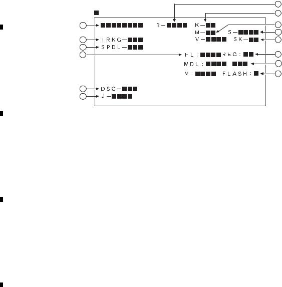
|
1 |
|
2 |
|
3 |
|
4 |
|
|
|
|
|
|
6.2 DISPLAY SPECIFICATION OF THE TEST MODE
A |
|
Character in bold : Item name |
2 |
|
|
: Information display |
3 |
1 |
7 |
|
8 |
5 |
9 |
6 |
|
12 |
13 |
|
14 |
B |
15 |
|
|
10 |
|
11 |
|
1 Address indication
The address being traced is displayed in number.
C
(as for the DVD, indication of decimal number is possible.) DVD : ID indication (hexadecimal number, 8 digits)
|
[* * * * * * * *] |
CD : ID indication |
[* * * * * * * *] |
2 Code indication of remote control unit [R – * * * *]
In case of double code, display a 2nd code.
3 Main unit keycode indication [K – * *]
5 Tracking status [TRKG – * * *]
|
Tracking on : [ON] |
D |
Tracking off : [OFF] |
|
6 Spindle status [SPDL – * * *]
CLV : [CLV]
Off : [OFF]
7 Mechanism (loading) position value [M – * *]
Unknown |
: [01] or [41] |
Open state |
: [04] |
Close state |
: [08] |
During opening |
: [12] |
During closing |
: [22] |
E
a Disc sensing [DSC – * * *]
The type of discs loaded is displayed. [DVD], [CD ]
b Jitter value [J – * * * *]
Note: Don't use it.
c Version of the FL controller [FL: * * * *]
Note: Don't use it.
d Region setting of the player [REG: *]
Setting value : [1] to [6]
e Destination setting of the FL controller [MDL: * * * * / * * *]
Four characters in the front represent code 01.
Three characters in the back represent the destination code. J: /J, K: /KU, /KC, /KU/KC, R: /RL/RD, RAM : /RAM, LB: /LB, WY: /WY
f Version of the flash ROM [V: * *. * *] Flash ROM size [FLASH = * *]
8 Slider position [S – * * * *]
In Side Switch ON : [01] In Side Switch OFF : [00]
9 Output video system [V – * * * *]
|
NTSC system |
: [NTSC] |
|
||
|
PAL system |
: [PAL] |
Automatic setting : [AUTO]
Scart terminal output [SK – * *]
(Display only the WY model which can do the output setting of scart terminal.)
FVIDEO : [00] S-VIDEO : [01]
RGB : [02]
26 |
|
|
|
|
|
|
|
|
|
|
|
|
XV-DV363 |
|
|
|
|
||||
|
1 |
|
2 |
|
|
|
3 |
|
4 |
|
|
|
|
|
|
|
|
||||

|
5 |
|
6 |
|
7 |
|
8 |
|
|
|
|
|
|
6.3 FUNCTIONAL SPECIFICATION OF THE SHORTCUT KEY
Only during normal playback, the following shortcut keys can be assigned by pressing a required key after pressing the ESC key of the remote control unit. To quit, press the ESC key
Command Contents |
Conditions |
Remote Control |
Remote |
|
Key Name |
Control Code |
|||
|
|
|||
Memory clear and region / revision indication |
|
CLEAR (*1) |
A8-45 |
|
Average value measurement of DVD error rate |
|
5 (*1) |
A8-05 |
|
CD error rate measurement |
|
5 (*1) |
A8-05 |
|
Scart terminal output : VIDEO |
|
AUDIO |
A3-BE |
|
Scart terminal output : S-VIDEO |
WY, models equipped with Scart terminal |
SUBTITLE |
A3-36 |
|
Scart terminal output : RGB |
|
ANGLE |
A3-B5 |
|
Progressive OFF |
Only for progressive models |
R_SKIP |
A3-9D |
|
Progressive ON |
F_SKIP |
A3-9C |
||
|
||||
HDMI Resolution : 1920 x 1080i |
Only for HDMI models |
PROGRAM |
A3-EC |
|
FL indication of ID number |
|
STEREO (*1) |
A8-4A |
|
ZOOM ON (x4) |
|
ZOOM |
A3-37 |
|
Service mode indication (error rate indication, etc.) |
|
CHP/TIM (*1) |
A8-13 |
|
Model information indication |
|
CHAP (*1) |
A8-40 |
|
Title search Input mode IN |
|
SIDE A (*1) |
A8-4D |
|
Title No. input |
|
Numbers (*1) |
A8-00 to A8-09 |
|
Search execution |
|
PLAY (*1) |
A8-17 |
|
Region confimation mode |
|
A.MON (*1) |
A8-1E |
|
|
Numbers (*1) |
A8-01 to A8-08 |
||
|
|
*1 : Test mode remote control unit
A
B
C
 Service mode indication (ESC + CHP/TIM keys)
ID Address
The error rate is always displayed in exponential notation, e.g., *.* * e - *, for both DVDs and CDs.
EDC/ID/AV 1 error history (ID Address, EDC/ID Error, last eight errors)
 Calculation of the average error rate (ESC + "5" [Test mode remote control unit] keys)
The average of the last eight error rates is calculated and indicated in exponential notation. After the calculation is completed, "OK" or "NG" is |
|
displayed. If "NG" is displayed, the disc tray will open (for both DVDs and CDs) |
|
For DVDs: OK with 5.0e-4 or less, for CDs: OK with 7.6e-3 or less |
D |
 Indication of model information (ESC + CHAP keys)
The items from 12 to 15 of the TEST MODE Indications are displayed. However, in the indications, S in the standard test mode is changed to CHIP VERSION, and M is changed to RF VERSION. For details, see 6.4.
 Region confirmation mode (ESC + A.MON [Test mode remote control unit] + "1"-"8" [Test mode remote control unit] keys)
After you press the AUDIO key while holding the ESC key pressed and then input the region number, if the number is different from that set in the unit, an error message is displayed, and the tray opens.
E
F
|
|
|
|
|
|
|
|
27 |
|
|
|
|
|
|
XV-DV363 |
|
|
||||
|
|
|
|
|
|
|
|
|||
|
5 |
|
6 |
|
|
|
7 |
|
8 |
|
|
|
|
|
|
|
|
||||

|
1 |
|
2 |
|
3 |
|
4 |
|
|
|
|
|
|
6.4 SPECIFICATION OF MODEL INFORMATION DISPLAY
A
To display model information : Press the ESC key then the CHAP key.
To close the model information display : Press the ESC key.
• Display contents |
|
|
1 |
|
10 |
B |
|
9 |
2 |
|
|
Don't care. |
|
3


4
5


6
7
C |
Character in bold : Item name |
|
: Information display |
||
|
1 Destination indication
Display it according to model information set from the FL controller.
2 Region No.
3 Part number
4 ROM version
5 Flash size
D
6 FL controller version
7 CHIP VERSION
9 Remote control code
0 Key code of Main unit
E
F
28 |
|
|
|
|
|
|
|
|
|
|
|
|
XV-DV363 |
|
|
|
|
||||
|
1 |
|
2 |
|
|
|
3 |
|
4 |
|
|
|
|
|
|
|
|
||||

|
5 |
|
6 |
|
7 |
|
8 |
|
|
|
|
6.5 FUNCTIONAL SPECIFICATION OF THE SERVICE MODE
• Display during Service Mode
To enter Service Mode, press the CHP/TIM key while holding the ESC key pressed. To quit, press the ESC key.
Service mode display
1 ID Address
2 Error rate (always displayed), in exponential notation
ERROR RATE :
( )
Number of error
• Calculation of the average error rate
For DVDs: OK with 5.0e-4 or less, for CDs: OK with 7.6e-3 or less
ex) For DVDs |
|
|
|
• Step 1 |
|
• Step 2 |
|
""e - |
|
""e -4 |
|
""e -6 : OK |
3.0e -4 : OK |
||
""e -5 : OK |
4.0e -4 : OK |
||
""e -4 : Refer to Step 2 |
5.0e -4 |
: OK |
|
""e -3 |
: NG |
6.0e -4 |
: NG |
""e -2 |
: NG |
7.0e -4 |
: NG |
3 EDC/ID error history (ID Address, EDC/ID errors, last eight errors)
Note:
Error of AV1 is not supported in this player.
Indication plan contents


 3 1
3 1 


 2
2 


A
B
C
D
|
|
Character in bold : Item name |
E |
: Information display |
|
|
|
|
|
F
|
|
|
|
|
|
|
|
29 |
|
|
|
|
|
|
XV-DV363 |
|
|
||||
|
|
|
|
|
|
|
|
|||
|
5 |
|
6 |
|
|
|
7 |
|
8 |
|
|
|
|
|
|
|
|
||||

|
1 |
|
2 |
|
3 |
|
4 |
|
|
|
|
|
|
6.6 SERVICE TEST MODE
A
1. Conditions During Service Test Mode
•During Service Test mode, the unit will not be shut down for an emergency even if one of the failures mentioned below occurs.
•After the unit has been shut down in Normal mode for an emergency upon detection of one of the failures mentioned below, you can turn it on immediately, without waiting for one minute, in Service Test mode.
• The accumulated power-on time can be checked during Service Test mode.
2. How to enter Service Test mode
•Connect AC power cord with the STEST port (microcomputer terminal IC5501: 43-pin) at High (5 V). (See "Service Test mode connecting point".)
Note: Initial function setting is DVD/CD.
B• Connect AC power cord while holding both the PLAY LIST 3 and POWER keys on the main unit pressed. The unit will be turned on, and the following indication will be displayed: Service Test mode starts, as follows:
Note: If the power cord was disconnected immediately before, be sure to wait at least one minute before turning on the power in the manner mentioned above. Otherwise, the unit may not operate properly.
|
Service Test Mode connecting point |
|
|
|
|
|||||||
|
Q55341/2 Q5533 |
Q5535 |
|
|
|
|
5547 UTEST |
R5542R5541 STEST |
|
|
|
B |
|
|
- FLDC FLDC+ |
|
1 |
|
|
5546 |
50 |
|
|
||
|
|
|
|
|
V+10 |
|
|
|
|
|
|
|
|
|
|
|
R5543 |
|
|
R5545 |
|
51 |
|
||
|
|
|
R5530 |
|
|
|
|
|
|
|
|
|
|
|
|
Q5532 |
NP |
R5528 |
C1413 |
|
|
|
C5555 |
|
|
|
Connecting point |
|
Q5531 |
D1417 |
R5548 |
R5557 |
||||||
|
|
|
|
|
|
|||||||
C |
|
|
|
|
|
|
||||||
|
|
|
|
|
R1415 |
V+3R3 |
|
|
|
|||
|
|
|
|
|
|
|
D1416 |
|
|
|
|
|
|
|
|
|
|
|
|
C1415 |
Q1402 |
D1403 |
|
C5558 |
|
|
|
|
|
|
|
|
Q1413 |
|
4 |
R5 |
||
|
|
|
|
|
|
|
D1415 |
|
|
|
1 |
|
|
|
D |
|
|
KN5601 |
|
R1403 |
|
IC5502 |
5 |
8R5559 |
|
|
|
|
|
|
|
|
|
R1401 |
|
|
|
|
|
|
|
|
|
|
|
|
[[ G ]] |
|
R1404 |
C5557 |
|
|
|
|
|
|
|
|
A30C5/C7 |
R1402 |
|
|||
DVD MAIN ASSY
SIDE A
3. Indications on the FL display when Service Test mode is entered
•Indications on the FL display when Service Test mode is entered differ depending on whether the unit was turned off normally or shut down for emergency protection, immediately before Service Test mode starts, as follows:
D
[After a normal power-off]
FL display W E L C O M E
|
FL display |
V O L |
0 |
|
|
|
|
|
|
|
FL display |
D V D |
S E R V |
|
|
|
|
|
|
[After a shutdown caused |
|
[After a shutdown caused |
[After a shutdown caused |
||||||
by an AMP-system failure] |
|
by a DVD-system failure] |
by an EEPROM (IC5502) failure] |
||||||
FL display |
P R T C T |
E |
FL display D V D P R T C T |
FL display |
E E P |
E R R |
|||
FL display |
V O L |
|
0 |
FL display |
V O L |
0 |
FL display |
V O L |
0 |
E |
|
|
|
|
|
|
|
|
|
FL display |
D V D |
S E R V |
FL display |
D V D |
S E R V |
FL display |
D V D |
S E R V |
|
[After a shutdown caused |
|
[After a shutdown 1 caused |
[After a shutdown 2 caused |
||||||
by high-temperature detection] |
by over current detection] |
by over current detection] |
|||||||
FL display |
O V E R T E M P |
FL display |
O C E R R 1 |
FL display |
O C E R R 2 |
||||
FL display |
V O L |
|
0 |
FL display |
V O L |
0 |
FL display |
V O L |
0 |
FL display |
D V D |
S E R V |
FL display |
D V D |
S E R V |
FL display |
D V D |
S E R V |
|
F4. How to quit Service Test mode, and conditions for quitting
•To quit Service Test mode, turn the power off or disconnect the AC power cord to turn the power off.
•When Service Test mode is quit, only data on protection in RAM will be initialized, and data on user settings in RAM will not be initialized.
30 |
|
|
|
|
|
|
|
|
|
|
|
|
XV-DV363 |
|
|
|
|
||||
|
1 |
|
2 |
|
|
|
3 |
|
4 |
|
|
|
|
|
|
|
|
||||
Loading...