


 Loading...
|
RM-84/99 |
Nokia Customer Care |
System Module |
(This page left intentionally blank.)
Page 1–2 |
Company Confidential |
Issue 1 |
|
Copyright ©2005 Nokia. All Rights Reserved. |
|

RM-84/99 |
|
System Module |
Nokia Customer Care |
|
Table of Contents |
|
Baseband description.................................................................................................................................................................... |
|
1–7 |
System module block diagram............................................................................................................................................. |
|
1–7 |
Baseband functional description......................................................................................................................................... |
|
1–8 |
Absolute maximum ratings................................................................................................................................................. |
|
1–10 |
Phone modes of operation.................................................................................................................................................. |
|
1–10 |
Power distribution................................................................................................................................................................. |
|
1–14 |
Clocking scheme...................................................................................................................................................................... |
|
1–16 |
Bluetooth/FM module............................................................................................................................................................ |
|
1–17 |
USB............................................................................................................................................................................................... |
|
1–17 |
SIM interface............................................................................................................................................................................. |
|
1–17 |
RS MMC interface..................................................................................................................................................................... |
|
1–18 |
Battery interface..................................................................................................................................................................... |
|
1–19 |
Camera interfaces................................................................................................................................................................... |
|
1–19 |
Back camera....................................................................................................................................................................... |
|
1–19 |
Camera construction........................................................................................................................................................ |
|
1–20 |
Back camera slider detection switch.......................................................................................................................... |
|
1–22 |
Flash LED.............................................................................................................................................................................. |
|
1–23 |
Front camera...................................................................................................................................................................... |
|
1–24 |
User interface........................................................................................................................................................................... |
|
1–25 |
Display interface................................................................................................................................................................ |
|
1–25 |
Keyboard.............................................................................................................................................................................. |
|
1–26 |
Display and keyboard backlight................................................................................................................................... |
|
1–28 |
ALS interface....................................................................................................................................................................... |
|
1–29 |
ASICs............................................................................................................................................................................................ |
|
1–30 |
RAP3G ASIC.......................................................................................................................................................................... |
|
1–30 |
Retu EM ASIC....................................................................................................................................................................... |
|
1–30 |
Tahvo EM ASIC..................................................................................................................................................................... |
|
1–30 |
Device memories..................................................................................................................................................................... |
|
1–30 |
RAP3G memories NOR flash and SDRAM.................................................................................................................... |
1–30 |
|
Combo memory................................................................................................................................................................. |
|
1–31 |
Audio concept................................................................................................................................................................................ |
|
1–31 |
Audio HW architecture.......................................................................................................................................................... |
|
1–31 |
Internal microphone.............................................................................................................................................................. |
|
1–32 |
External microphone............................................................................................................................................................. |
|
1–32 |
Internal earpiece..................................................................................................................................................................... |
|
1–33 |
Internal speaker...................................................................................................................................................................... |
|
1–33 |
External earpiece.................................................................................................................................................................... |
|
1–34 |
Vibra circuitry........................................................................................................................................................................... |
|
1–34 |
Pop-portTM connector........................................................................................................................................................... |
|
1–35 |
Baseband technical specifications.......................................................................................................................................... |
|
1–36 |
External interfaces.................................................................................................................................................................. |
|
1–36 |
External interfaces............................................................................................................................................................ |
|
1–36 |
ACI interface electrical characteristics........................................................................................................................ |
|
1–36 |
VOUT electrical characteristics...................................................................................................................................... |
|
1–37 |
USB IF electrical characteristics.................................................................................................................................... |
|
1–37 |
FBUS interface electrical characteristics.................................................................................................................... |
1–38 |
|
Headset hook detection interface (XMICN) electrical characteristics............................................................... |
1–38 |
|
Audio signal electrical characteristics........................................................................................................................ |
|
1–39 |
SIM IF connections............................................................................................................................................................ |
|
1–39 |
RS MMC interface connections....................................................................................................................................... |
|
1–39 |
Issue 1 |
Company Confidential |
Page 1–3 |
Copyright ©2005 Nokia. All Rights Reserved. |
|
|

|
|
RM-84/99 |
Nokia Customer Care |
|
System Module |
Charger connector and charging interface connections & electrical characteristics.................................. |
1–40 |
|
Battery connector and interface connections & electrical characteristics...................................................... |
1–41 |
|
Internal interfaces.................................................................................................................................................................. |
|
1–41 |
Internal interfaces............................................................................................................................................................ |
|
1–41 |
UI module connector and IF connections................................................................................................................. |
1–42 |
|
Keyboard interface electrical characteristics........................................................................................................... |
1–43 |
|
Display connector and interface connections.......................................................................................................... |
1–44 |
|
Camera interface connections and electrical characteristics.............................................................................. |
1–45 |
|
Front camera interface and electrical characteristics........................................................................................... |
1–47 |
|
Flash LED interface and electrical characteristics................................................................................................... |
1–49 |
|
Slider switch electrical characteristics....................................................................................................................... |
|
1–50 |
Back-up battery interface connections and electrical characteristics.............................................................. |
1–50 |
|
RF description................................................................................................................................................................................ |
|
1–50 |
Receiver...................................................................................................................................................................................... |
|
1–50 |
Introduction to receiver functionality........................................................................................................................ |
|
1–50 |
WCDMA receiver................................................................................................................................................................. |
|
1–50 |
GSM receiver........................................................................................................................................................................ |
|
1–51 |
Transmitter............................................................................................................................................................................... |
|
1–51 |
Introduction to transmitter functionality................................................................................................................. |
1–51 |
|
WCDMA transmitter.......................................................................................................................................................... |
|
1–51 |
GSM transmitter................................................................................................................................................................. |
|
1–53 |
Frequency synthesizers......................................................................................................................................................... |
|
1–56 |
Regulators................................................................................................................................................................................. |
|
1–57 |
Frequency mappings................................................................................................................................................................... |
|
1–58 |
EGSM900 frequencies............................................................................................................................................................. |
|
1–58 |
GSM1800 frequencies............................................................................................................................................................ |
|
1–59 |
GSM1900 frequencies............................................................................................................................................................ |
|
1–60 |
WCDMA Rx frequencies.......................................................................................................................................................... |
|
1–61 |
WCDMA Tx frequencies.......................................................................................................................................................... |
|
1–62 |
List of Tables |
|
|
Table 1 Camera specifications.................................................................................................................................................. |
|
1–20 |
Table 2 Keymatrix......................................................................................................................................................................... |
|
1–26 |
Table 3 LED driver control signals............................................................................................................................................ |
|
1–29 |
Table 4 ALS resistor values......................................................................................................................................................... |
|
1–29 |
Table 5 Audio connector pin assignments........................................................................................................................... |
|
1–35 |
Table 6 Charging interface connections................................................................................................................................ |
|
1–40 |
Table 7 Charging IF electrical characteristics....................................................................................................................... |
|
1–40 |
Table 8 Battery interface connections................................................................................................................................... |
|
1–41 |
Table 9 Battery IF electrical characteristics.......................................................................................................................... |
|
1–41 |
Table 10 User interface connections...................................................................................................................................... |
|
1–42 |
Table 11 Display interface connections................................................................................................................................. |
|
1–44 |
Table 12 Camera interface connections................................................................................................................................ |
|
1–45 |
Table 13 Camera CCP IF electrical characteristics............................................................................................................... |
1–46 |
|
Table 14 Camera supply voltage characteristics................................................................................................................. |
1–47 |
|
Table 15 Camera control IF electrical characteristics........................................................................................................ |
1–47 |
|
Table 16 Front camera interface connections..................................................................................................................... |
1–47 |
|
Table 17 Front camera voltage levels from Helen point of view................................................................................... |
1–49 |
|
Table 18 Front camera voltage levels from camera module point of view............................................................... |
1–49 |
|
Table 19 Front camera supply voltage characteristics...................................................................................................... |
1–49 |
|
Table 20 Flash LED interface connections............................................................................................................................. |
|
1–49 |
Page 1–4 |
Company Confidential |
Issue 1 |
Copyright ©2005 Nokia. All Rights Reserved. |
|
|

RM-84/99 |
|
System Module |
Nokia Customer Care |
Table 21 Flash LED interface electrical characteristics ..................................................................................................... |
1–50 |
Table 22 Back-up battery connections................................................................................................................................... |
1–50 |
Table 23 Back-up battery electrical characteristics........................................................................................................... |
1–50 |
List of Figures |
|
Figure 1 System level block diagram........................................................................................................................................ |
1–7 |
Figure 2 Functional block diagram............................................................................................................................................ |
1–8 |
Figure 3 OMAP1710 high level block diagram....................................................................................................................... |
1–9 |
Figure 4 State diagram............................................................................................................................................................... |
1–12 |
Figure 5 Power distribution diagram..................................................................................................................................... |
1–14 |
Figure 6 System start-up timing.............................................................................................................................................. |
1–16 |
Figure 7 Clocking scheme........................................................................................................................................................... |
1–17 |
Figure 8 SIM interface.................................................................................................................................................................. |
1–18 |
Figure 9 MMC interface................................................................................................................................................................ |
1–18 |
Figure 10 Battery pin order....................................................................................................................................................... |
1–19 |
Figure 11 Block diagram of the back camera module...................................................................................................... |
1–20 |
Figure 12 Camera module cross section and assembly principle.................................................................................. |
1–21 |
Figure 13 Camera module bottom view including serial numbering.......................................................................... |
1–21 |
Figure 14 Slider switch connection......................................................................................................................................... |
1–23 |
Figure 15 Simplified flash LED connection............................................................................................................................ |
1–24 |
Figure 16 Front camera connections...................................................................................................................................... |
1–25 |
Figure 17 General diagram of the LCD module................................................................................................................... |
1–25 |
Figure 18 Keyboard layout......................................................................................................................................................... |
1–28 |
Figure 19 ALS HW implementation......................................................................................................................................... |
1–29 |
Figure 20 Audio block diagram................................................................................................................................................ |
1–32 |
Figure 21 Internal microphone circuitry............................................................................................................................... |
1–32 |
Figure 22 External microphone circuitry (Pop-Port connects to the right side)....................................................... |
1–33 |
Figure 23 Internal earpiece circuitry...................................................................................................................................... |
1–33 |
Figure 24 Internal speaker circuitry........................................................................................................................................ |
1–34 |
Figure 25 External earpiece circuitry (Pop-Port connected on the right)................................................................... |
1–34 |
Figure 26 Vibra circuitry............................................................................................................................................................. |
1–35 |
Figure 27 External audio connector........................................................................................................................................ |
1–35 |
Figure 28 Charger connector..................................................................................................................................................... |
1–40 |
Figure 29 Battery connector...................................................................................................................................................... |
1–41 |
Figure 30 UI connector................................................................................................................................................................ |
1–42 |
Figure 31 Display connector...................................................................................................................................................... |
1–44 |
Figure 32 WCDMA transmitter................................................................................................................................................... |
1–52 |
Figure 33 Block diagram of DCDC converter and WCDMA PA........................................................................................... |
1–53 |
Figure 34 GSM transmitter......................................................................................................................................................... |
1–54 |
Figure 35 GSM/EDGE power control topology and control signals................................................................................ |
1–55 |
Figure 36 Power control signal usage in GSM (GMSK) and EDGE (8PSK) transmission............................................ |
1–55 |
Figure 37 Phase locked loop in N7500 and N7501 (PLL).................................................................................................. |
1–56 |
Figure 38 RF supply connections from the BB mixed mode ASIC.................................................................................. |
1–57 |
Issue 1 |
Company Confidential |
Page 1–5 |
|
Copyright ©2005 Nokia. All Rights Reserved. |
|

|
RM-84/99 |
Nokia Customer Care |
System Module |
(This page left intentionally blank.)
Page 1–6 |
Company Confidential |
Issue 1 |
|
Copyright ©2005 Nokia. All Rights Reserved. |
|
RM-84/99 |
|
System Module |
Nokia Customer Care |
 Baseband description
System module block diagram
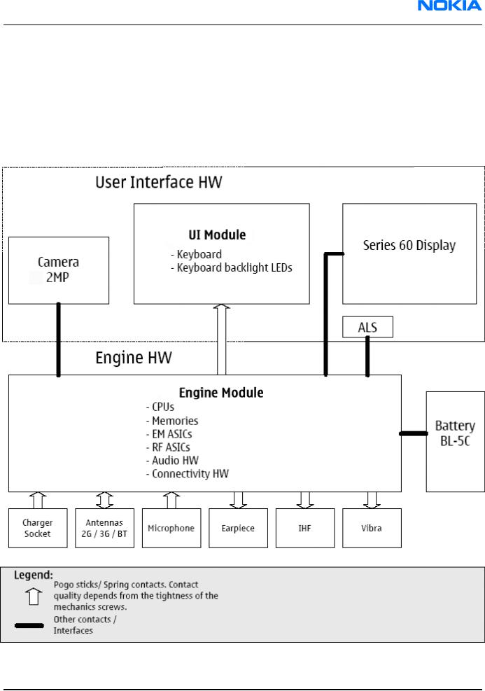
The device consists of two different main modules: transceiver and UI. The transceiver board consists of baseband and RF components. The UI board consists of key domes and keypad backlights. Connection between the UI and the transceiver board is established via a board-to-board spring connector.
Note: In this description, the user interface HW covers display, camera, keyboard, keyboard backlight and ALS.
|
Figure 1 System level block diagram |
|
Issue 1 |
Company Confidential |
Page 1–7 |
|
Copyright ©2005 Nokia. All Rights Reserved. |
|
|
RM-84/99 |
Nokia Customer Care |
System Module |
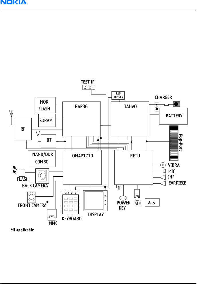
Baseband functional description
Digital baseband consists of an ISA (Intelligent Software Architecture) based modem and Symbian based application sections. The modem functionality is in RAP3G, and OMAP acts as a platform for Symbian applications. The terms ISA and Symbian are used refer to the software environment of these devices.
The modem section consists of a RAP3G ASIC with NOR FLASH and SDRAM memory as the core. RAP3G supports cellular protocols of WCDMA (3GPP R-4) and GSM (EDGE class 10, GPRS phase2). The modem SDRAM memory has 64Mbits of memory and NOR flash has 64Mbits of memory. RAP3G operates with the system clock of 38.4 MHz, which comes from the VCTCXO.
The application section includes an OMAP ASIC with DDR/NAND combo memory as the core. The OMAP ASIC uses a 19.2MHz clock, which comes from the RAP3G divided by two from the 38.4 MHz system clock.
Figure 2 Functional block diagram
OMAP processor (Helen3 (OMAP1710)) is also called an application ASIC because it is processing application SW and handles the UI SW. It consists of OMAP3.3 and peripheral subsystems such as camera, display and keyboard driver blocks.
Page 1–8 |
Company Confidential |
Issue 1 |
|
Copyright ©2005 Nokia. All Rights Reserved. |
|
RM-84/99 |
|
System Module |
Nokia Customer Care |
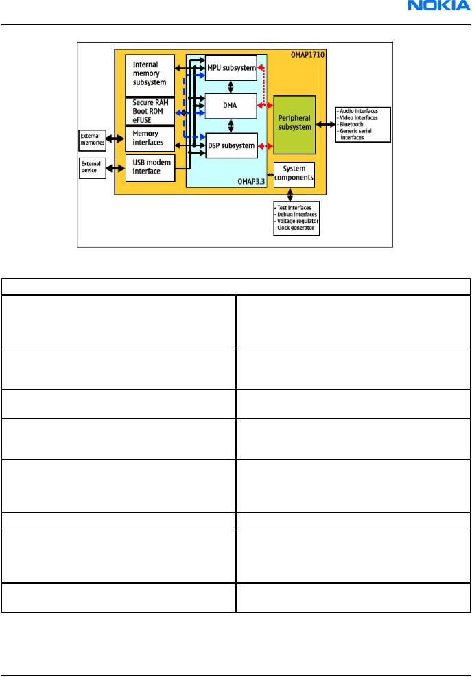
Figure 3 OMAP1710 high level block diagram |
|
|
|
Section |
Description |
|
|
Helen3 (OMAP1710) processor |
also called an application ASIC because it is |
|
processing application SW and handles the UI SW. It |
|
consists of OMAP3.3 and peripheral subsystems like |
|
camera, display and keyboard driver blocks. |
OMAP3.3 |
consists of ARM926 (MPU subsystem), TMS320C55x |
|
(DSP subsystem), DMA and OMAP3.3s internal |
|
peripherals. |
Helen3 (OMAP1710) MPU subsystem |
based on an ARM926EJ. MPU is able to perform most |
|
of the application operations on the chip. |
System DMA component |
mainly used to help the MPU and DSP perform data |
|
memory transfer-specific tasks, leaving more |
|
available MIPS for both processors. |
DSP subsystem |
based on a TMS320C55x™ DSP core, which is |
|
responsible for intensive data computing tasks like |
|
real-time audio and video handling on application |
|
side, e.g. voice recording. |
Internal memory subsystem |
composed of a single port SRAM. |
Secure modules |
Helen3 (OMAP1710) contains a set of several |
|
components, including ROM, a single port SRAM, and |
|
eFUSE cells. These components enable the system to |
|
support secure applications. |
Memory interfaces |
The memory interfaces define the system memory |
|
access organization of Helen3 (OMAP1710). |
Issue 1 |
Company Confidential |
Page 1–9 |
|
Copyright ©2005 Nokia. All Rights Reserved. |
|
|
RM-84/99 |
Nokia Customer Care |
System Module |
|
|
Section |
Description |
|
|
USB & modem interface |
These two modules enable the platform to support a |
|
universal serial link and a dedicated modem |
|
interface, enabling a high data transfer rate between |
|
the modem and the application chip. |
System components |
System components are group of modules |
|
responsible for managing system interactions such |
|
as interrupt, clock control and idle. |
Peripheral subsystem |
The peripheral subsystem defines all the |
|
components used to interface Helen3 (OMAP1710) |
|
with specific external devices such as camera, |
|
keyboard, display, etc. |
Absolute maximum ratings
Signal |
Min |
Nom |
Max |
Unit |
Notes |
Battery voltage (idle) |
-0.3 |
|
+4.5 |
V |
Battery voltage maximum value is |
|
|
|
|
|
specified during charging is active |
Battery voltage (Call) |
+3. |
|
+4.3 |
V |
Battery voltage maximum value is |
|
2 |
|
|
|
specified during charging is active |
Charger input voltage |
-0.3 |
|
+16V |
V |
|
Back-Up supply voltage |
0 |
2.5 |
2.7 |
V |
Maximum capacity of the backup |
|
|
|
|
|
power supply assumed to be 15 µAh. |
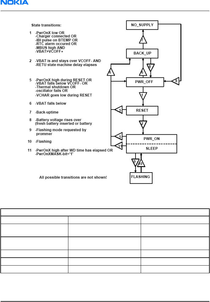
Phone modes of operation
Mode |
Description |
NO_SUPPLY |
(dead) mode means that the main battery is not present or its voltage is too low (below |
|
RETU master reset threshold) and that the back-up battery voltage is too low. |
BACK_UP |
The main battery is not present or its voltage is too low but back-up battery voltage is |
|
adequate and the 32kHz oscillator is running (RTC is on). |
PWR_OFF |
In this mode (warm), the main battery is present and its voltage is over RETU master reset |
|
threshold. All regulators are disabled, PurX is on low state, the RTC is on and the oscillator |
|
is on. PWR_OFF (cold) mode is almost the same as PWR_OFF (warm), but the RTC and the |
|
oscillator are off. |
RESET |
RESET mode is a synonym for start-up sequence. In this mode certain regulators are |
|
enabled and after they and RFClk have stabilized, the system reset (PurX) is released and |
|
PWR_ON mode entered. RESET mode uses 32kHz clock to count the REST mode delay |
|
(typically 16ms). |
Page 1–10 |
Company Confidential |
Issue 1 |
|
Copyright ©2005 Nokia. All Rights Reserved. |
|
RM-84/99 |
|
|
System Module |
|
Nokia Customer Care |
|
|
|
Mode |
Description |
|
|
|
|
SLEEP |
SLEEP mode is entered only from PWR_ON mode with the aid of SW when the system’s |
|
|
activity is low. There are in principle three different sleep modes: |
|
|
• |
OMAP1710 sleep |
|
• |
RAP3G sleep |
|
• OMAP and RAP3G sleep (deep sleep) |
|
|
In SLEEP mode RETU’s regulators VIO, VDRAM, VSIM1, VSIM2, VAUX and Vana are in low |
|
|
quiescent current mode (output voltages still present but regulators will not give as much |
|
|
current out). Other regulators including VR1 supplying system clock oscillator are |
|
|
disabled. |
|
|
In SLEEP mode, TAHVO VCORE SMPS regulator is in low quiescent current mode (if sleep |
|
|
mode is not internally disabled). Linear regulator VOUT state depends on the accessory |
|
|
connected to the system connector (Pop-Port), if there is any. |
|
FLASHING |
FLASHING mode is for SW downloading. FLASHING mode is not really a RETU or TAHVO |
|
|
state but rather a system state. From RETU and TAHVO point of view, it is like PWR_ON. |
|
|
The state is entered from PWR_ON. It is possible to use external voltage (VPP) during |
|
|
flashing to speed up the process (provided that the memory components support the |
|
|
feature). |
|
Issue 1 |
Company Confidential |
Page 1–11 |
|
Copyright ©2005 Nokia. All Rights Reserved. |
|
|
RM-84/99 |
Nokia Customer Care |
System Module |
|
Figure 4 State diagram |
|
Voltage limits |
|
|
|
|
|
Parameter |
Description |
Value |
|
|
|
VMSTR |
Master reset threshold (RETU) |
2.2V (typ.) |
|
Threshold for charging, rising |
|
VMSTR+ |
(TAHVO) |
2.1V (typ.) |
|
Threshold for charging, falling |
|
VMSTR- |
(TAHVO) |
1.9V (typ.) |
VCOFF+ |
Hardware cutoff (rising) |
2.9V (typ.) |
VCOFF- |
Hardware cutoff (falling) |
2.6V (typ.) |
SWCOFF |
SW cutoff limit |
~3.2V |
Page 1–12 |
Company Confidential |
Issue 1 |
|
Copyright ©2005 Nokia. All Rights Reserved. |
|

RM-84/99 |
|
System Module |
Nokia Customer Care |
The master reset threshold controls the internal reset of Retu / (Tahvo). If battery voltage is above VMSTR, Tahvo’s charging control logic is alive. Also, RTC is active and supplied from the main battery. Above VMSTR, Tahvo allows the system to be powered on although this may not succeed due to voltage drops during start up. SW can also consider battery voltage too low for operation and power down the system.
Power key
The system boots up when power key is pressed (adequate battery voltage, VBAT, present).
Power down can be initiated by pressing the power key again (the system is powered down with the aid of SW). Power on key is connected to Retu ASIC via PWRONX signal.
Issue 1 |
Company Confidential |
Page 1–13 |
|
Copyright ©2005 Nokia. All Rights Reserved. |
|

|
RM-84/99 |
Nokia Customer Care |
System Module |
Power distribution
|
|
Figure 5 Power distribution diagram |
|
Power supply components: |
|
|
|
• |
RETU |
|
|
• |
TAHVO |
|
|
• |
Helen VCORE SMPS |
|
|
• |
BT |
|
|
• |
LDO |
|
|
• |
camera LDO |
|
|
Page 1–14 |
Company Confidential |
Issue 1 |
|
|
|
Copyright ©2005 Nokia. All Rights Reserved. |
|

RM-84/99 |
|
System Module |
Nokia Customer Care |
• backlight SMPS |
|
All the above are powered by the main battery voltage. |
|
Battery voltage is also used on the RF side for power amplifiers (GSM PA & WCDMA PA) and for RF ASICs Hinku (Rx) & Vinku(Tx).
Discrete power supplies are used to generate 2.8V to BT, 1.5V for the camera IO voltage, 2.8V for the front camera IO voltage, 1.3V/1.5V for Helen 3 and 18V for the backlight LEDs.
The device supports both 1.8V/3V SIM cards which are powered by RETU / VSIM1. RETUs VSIM2 is used to power RS MMC 1.8V only. USB accessories which needs power from the device are powered by TAHVO / VOUT.
Because LED driver in TAHVO is not used, the external SMPS is used instead. External LED SMPS is still controlled by TAHVO and powered by battery voltage.
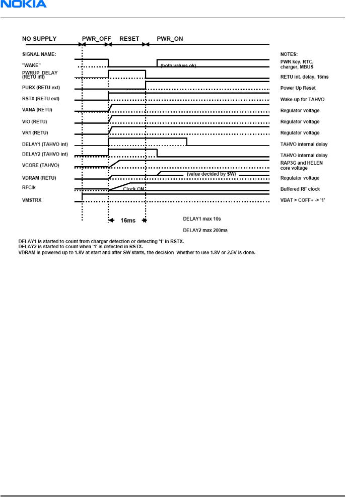
System power-up
After inserting the main battery, regulators started by HW are enabled. SW checks, if there is some reason to keep the power on. If not, the system is set to power off state by watchdog. Power up can be caused by the following reasons:
•Power key is pressed
•Charger is connected
•RTC alarm occurs
•MBUS wake-up After that:
•Retu activates sleep clock and VANA, VDRAM, VIO and VR1 regulators.
•Voltage appearing at Retu’s RSTX pin is used for enabling Tahvo ASIC.
•Tahvo enables VCORE regulator and its internal RC-oscillator (600kHz).
•VCTCXO regulator is set ON and RF clock (main system clock) is started to produce.
•Retu will release PURX ~ 16ms after power up is enabled (the RF clock is then stable enough).
•Synchronizing clock (2.4MHz) for Tahvo is started to be produced. After PURX is released and two rising edges of 2.4MHz synchronous clock have been detected in SMPSClk input Tahvo is starting to use that instead of 600kHz internal RC-oscillator.
•HW start-up procedure has been finalized and the system is up and running. Now it is possible for SW to switch ON other needed regulators.
Issue 1 |
Company Confidential |
Page 1–15 |
|
Copyright ©2005 Nokia. All Rights Reserved. |
|
|
RM-84/99 |
Nokia Customer Care |
System Module |
Figure 6 System start-up timing
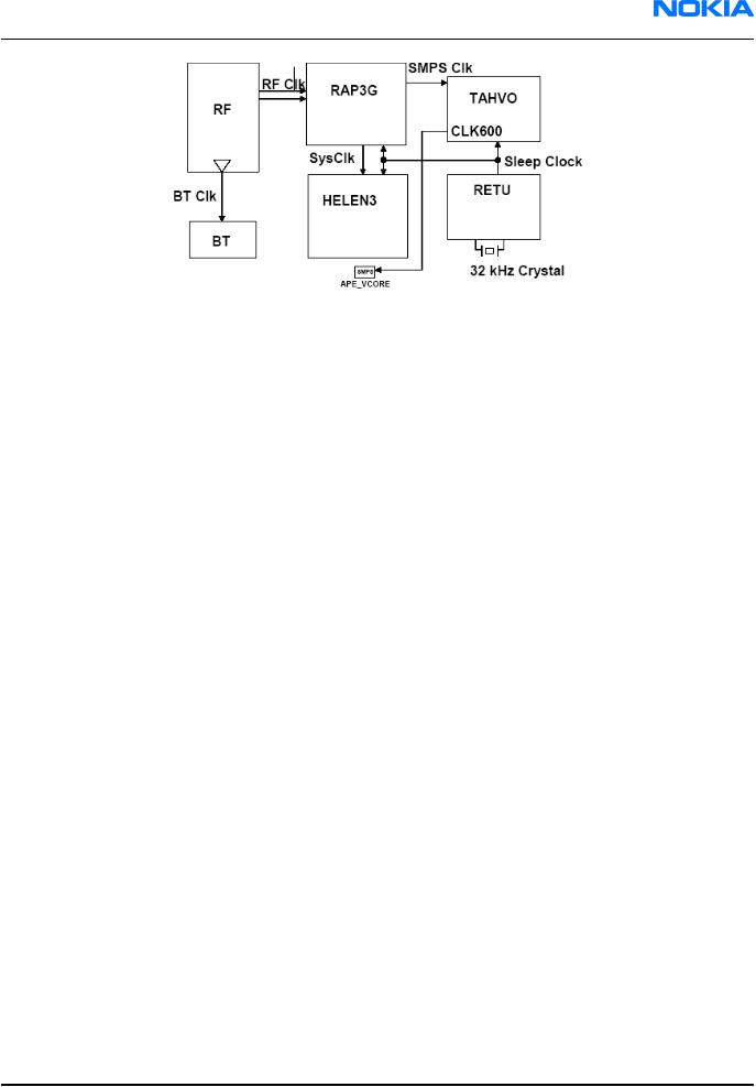
Clocking scheme
There are two main clocks in the system: 38.4MHz RF clock produced by VCTCXO in RF section and 32.768kHz sleep clock produced by RETU with an external crystal.
RF clock is generated only when VCTCXO is powered on by RETU regulator. Regulator itself is activated by SleepX signals from both RAP3G and Helen3. When both CPUs are on sleep, RF clock is stopped.
RF clock is used by RAP3G that then provides (divided) 19.2MHz SysClk further to OMAP. Both RAPG and Helen3 have internal PLLs which then create clock signals for other peripheral devices/interfaces like RS MMC, SIM, CCP, I2C and memories.
32k Sleep Clock is always powered on after startup. Sleep clock is used by RAP3G and OMAP for low-power operation.
SMPS Clk is 2.4MHz clock line from RAP3G to Tahvo used for switch mode regulator synchronizing in active mode. In deep sleep mode, when VCTCXO is off, this signal is set to '0'-state.
BT Clk is 38.4MHz signal from Hinku ASIC to the Bluetooth system.
CLK600 is 600KHz signal from Tahvo to APE VCORE SMPS. The clock source is internal RC oscillator in Tahvo (during the power-up sequence) or RAP3G SMPS Clk divided by 4 after the power-up sequence.
Page 1–16 |
Company Confidential |
Issue 1 |
|
Copyright ©2005 Nokia. All Rights Reserved. |
|
RM-84/99 |
|
System Module |
Nokia Customer Care |
Figure 7 Clocking scheme
Bluetooth/FM module
The Bluetooth and FM radio solutions of the device are realised with a combined BTFM module. This module has the Bluetooth solution and FM radio solution combined into a single component. However, the two solutions are electrically isolated from one another.
Bluetooth
Bluetooth provides a fully digital link for communication between a master unit and one or more slave units. The system provides a radio link that offers a high degree of flexibility to support various applications and product scenarios. Data and control interface for a low power RF module is provided. Data rate is regulated between the master and the slave.
The device Bluetooth is based on CSR's BC4 BT ASIC (BTHFM1.0).
The UART1 interface handles the transfer of control and data information between OMAP1710 and the BT system (BC4).
The PCM interface is used for audio data transfer between RAP3G and the BT system (BC4).
FM radio
The second part of the BTFM module contains the FM radio.
The antenna for the FM radio is provided by plugging in an external wired headset to the Pop-port™ connector. It is not possible to listen to the FM radio without a wired headset connected. The FM radio is controlled by I2C commands from RAP3G. The audio output of the FM radio is fed to the headset via the RETU ASIC, so the rest of the phone can sleep while the FM radio is active.
USB
USB (Universal Serial Bus) provides a wired connectivity between a USB host PC and peripheral devices.
USB is a differential serial bus for USB devices. USB controller (RAP3G) supports USB specification revision 2.0 with full speed USB (12 Mbps). The device is connected to the USB host through the Pop-Port™ connector. The USB bus is hot plugged capable, which means that USB devices may be plugged in/out at any time.
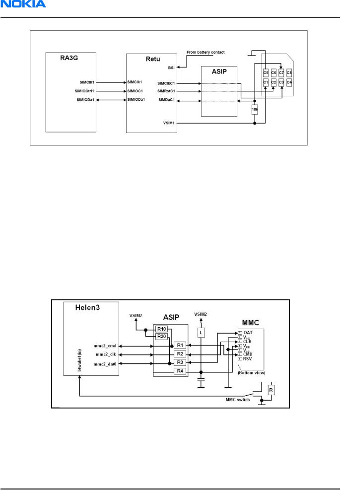
SIM interface
The device has one SIM (Subscriber Identification Module) interface. The SIM card is located under the battery. The SIM interface consists of an internal interface between RAP3G and Retu and of an external interface between Retu and SIM contacts. The main SIM interface functionality is in RAP3G while Retu takes care of power up/down, card detection, ATR (Answer To Reset) counting and level shifting. For Retu external SIM IF connections, see SIM interface connections (Page 1–39).
The SIM IF is shown in the following figure:
Issue 1 |
Company Confidential |
Page 1–17 |
|
Copyright ©2005 Nokia. All Rights Reserved. |
|
|
RM-84/99 |
Nokia Customer Care |
System Module |
Figure 8 SIM interface
Retu handles the detection of the SIM card. The detection method is based in the BSI line. Because of the location of the SIM card, removing the battery causes a quick power down of the SIM IF.
The Retu SIM1 interface supports both 1.8V and 3.0V SIM cards. The SIM interface voltage is first 1.8V when the SIM card is inserted, and if the card does not response to the ATR a 3V interface voltage is used.
The data communication between the card and the phone is asynchronous half duplex, and the clock supplied to the card is 1-5MHz, which is 3.2MHz by default (in GSM system). The data baud rate is the SIM card clock frequency divided by 372 (by default), 64, 32 or 16.
RS MMC interface
The reduced size (24mm x 18mm x 1.4mm) multimedia card slot is located under the battery. The device supports RS MMC hot insertion, which enables to remove/insert the card when the phone is powered on.
The RS MMC card is connected to the Helen3 processor MMC/SDIO2 (1.8V) interface. The MMC interface is shown in the following figure:
Figure 9 MMC interface
The basic multimedia card concept is based on the following communication signals: CLK, CMD and DAT.
With each cycle of the CLK signal, one bit transfer on the DAT and CMD line is performed. The maximum CLK frequency is 20MHz.
Page 1–18 |
Company Confidential |
Issue 1 |
|
Copyright ©2005 Nokia. All Rights Reserved. |
|
RM-84/99 |
|
System Module |
Nokia Customer Care |
CMD is a bi-directional command channel used for card initialization and data transfer commands. The CMD signal has two operational modes: open-drain and push-pull mode. The open-drain mode is used for card initialization and the push-pull mode for fast command transfer. CMD commands are sent by the host and CMD responses are sent by the card.
DAT is a bi-directional data channel, which operates in the push-pull mode.
The detection of the RS MMC card removal/insertion is done via the RS MMC cover switch. The RS MMC cover switch gives an interrupt to the SW when the cover is opened or closed. After opening the RS MMC cover lid (RS MMC SW signal is connected to GND via cover switch), SW powers down the card and switches off the RS MMC power supply (VSIM2). When the RS MMC cover lid is closed (RS MMC SW signal is internally connected in Helen3 to 1.8V), the card inserted is identified.
Note: Removing the RS MMC while writing to it, may corrupt the data stored in the card.
See Also
• RS MMC interface connections (Page 1–39)
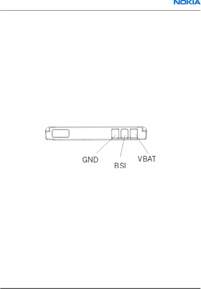
Battery interface
The battery interface supports the NMP 3-pole battery interface. The interface consists of three connectors: VBAT, BSI and GND.
The BSI line is used to recognize the battery capacity by a battery internal pull down resistor.
Figure 10 Battery pin order
Battery temperature is estimated by measuring separate battery temperature NTC via the BTEMP line, which is located on the transceiver PWB, at a place where the phone temperature is most stabile.
For service purposes, the device SW can be forced into local mode by using pull down resistors connected to the BSI line.
Camera interfaces
Back camera
The back camera of the device uses a 2.0 megapixel camera module with a sensor resolution of 1600 x 1200. The following block diagram shows how a CCP bus is used to transfer image data from the camera module to the phone engine. This bi-directional control bus is a software-implemented I2C interface.
The camera regulator N1470 powers the digital parts of the camera, and a VAUX power rail is used for powering the analogue parts.
A CAMVCTRL signal (Vctrl) is used for activating the camera module. When the Vctrl signal is High, the module enters the power on mode. When the signal is Low, the module enters the power off mode.
A CAMCLK signal feeds the system clock for the camera module.
Issue 1 |
Company Confidential |
Page 1–19 |
|
Copyright ©2005 Nokia. All Rights Reserved. |
|
Loading...