


NATIONAL SEMICONDUCTOR TMS427409ADJ-70, TMS427409ADJ-60, TMS427409ADJ-50, TMS427409ADGA-70, TMS427409ADGA-60 Datasheet
...TMS416409A, TMS417409A, TMS426409A, TMS427409A 4194304 BY 4-BIT EXTENDED DATA OUT DYNAMIC RANDOM-ACCESS MEMORIES
SMKS893B ± AUGUST 1996 ± REVISED APRIL 1997
This data sheet is applicable to all TMS41x409As and TMS42x409As symbolized by Revision ªBº, Revision ªEº, and subsequent revisions as described in the device symbolization section.
DOrganization . . . 4 194 304 × 4
DSingle Power Supply (5 V or 3.3 V)
DPerformance Ranges:
|
ACCESS ACCESS ACCESS |
EDO |
||
|
TIME |
TIME |
TIME |
CYCLE |
|
tRAC |
tCAC |
tAA |
tHPC |
|
MAX |
MAX |
MAX |
MIN |
'41x409A-50 |
50 ns |
13 ns |
25 ns |
20 ns |
'41x409A-60 |
60 ns |
15 ns |
30 ns |
25 ns |
'41x409A-70 |
70 ns |
18 ns |
35 ns |
30 ns |
'42x409A-50 |
50 ns |
13 ns |
25 ns |
20 ns |
'42x409A-60 |
60 ns |
15 ns |
30 ns |
25 ns |
'42x409A-70 |
70 ns |
18 ns |
35 ns |
30 ns |
DJ/DGA PACKAGES
( TOP VIEW )
|
VCC |
|
1 |
26 |
|
|
VSS |
||||
|
|
|
|
||||||||
|
|
||||||||||
DQ1 |
|
2 |
25 |
|
|
DQ4 |
|||||
DQ2 |
|
3 |
24 |
|
|
DQ3 |
|||||
|
|
|
|||||||||
|
|
|
|
|
|
|
|
|
|
|
|
|
|
W |
|
|
4 |
23 |
|
|
CAS |
||
|
|
|
|
|
|
|
|
|
|
|
|
|
RAS |
|
|
5 |
22 |
|
|
OE |
|
||
A11² |
|
6 |
21 |
|
|
A9 |
|||||
|
|
|
|||||||||
|
A10 |
|
8 |
19 |
|
|
A8 |
||||
|
|
|
|
||||||||
|
A0 |
|
9 |
18 |
|
|
A7 |
||||
|
|
|
|
||||||||
|
A1 |
|
10 |
17 |
|
|
A6 |
||||
|
|
|
|
||||||||
|
A2 |
|
11 |
16 |
|
|
A5 |
||||
|
|
|
|
||||||||
|
A3 |
|
12 |
15 |
|
|
A4 |
||||
|
|
|
|
||||||||
|
VCC |
|
13 |
14 |
|
|
VSS |
||||
|
|
|
|
||||||||
|
|
||||||||||
DExtended-Data-Out (EDO) Operation
DCAS-Before-RAS (CBR) Refresh
DLow Power Dissipation
D3-State Unlatched Output
DHigh-Reliability Plastic 24/26-Lead 300-Mil-Wide Surface-Mount Small-Outline J-Lead (SOJ) Package (DJ Suffix) and 24/26-Lead 300-Mil-Wide Surface-Mount Thin Small-Outline Package (TSOP)
(DGA Suffix)
DOperating Free-Air Temperature Range
0°C to 70°C
description
The TMS41x409A and TMS42x409A series are 16777216-bit dynamic random-access memory (DRAM) devices organized as 4194304 words of four bits each.
These devices feature maximum RAS access times of 50, 60, and 70 ns. All address and data-in lines are latched on chip to simplify system design. Data out is unlatched to allow greater system flexibility.
|
|
|
PIN NOMENCLATURE |
|
|
||
A0 ± A11² |
Address Inputs |
||
|
DQ1 ± DQ4 |
Data In / Data Out |
|
|
CAS |
Column-Address Strobe |
|
|
NC |
No Internal Connection |
|
|
OE |
Output Enable |
|
|
RAS |
|
Row-Address Strobe |
|
V |
5-V or 3.3-V Supply³ |
|
|
CC |
|
|
VSS |
Ground |
||
W |
Write Enable |
||
|
|
|
|
² A11 is NC for TMS417409A and TMS427409A. ³ See Available Options Table
AVAILABLE OPTIONS
|
|
SELF |
|
|
DEVICE |
POWER |
REFRESH, |
REFRESH |
|
SUPPLY |
BATTERY |
CYCLES |
||
|
||||
|
|
BACKUP |
|
|
|
|
|
|
|
TMS416409A |
5 V |
± |
4 096 in 64 ms |
|
|
|
|
|
|
TMS417409A |
5 V |
± |
2 048 in 32 ms |
|
|
|
|
|
|
TMS426409A |
3.3 V |
± |
4 096 in 64 ms |
|
|
|
|
|
|
TMS427409A |
3.3 V |
± |
2 048 in 32 ms |
The TMS416409A and TMS417409A are offered in a 24/26-lead plastic surface-mount SOJ package (DJ suffix). The TMS426409A and TMS427409A are offered in a 24/26-lead plastic surface-mount SOJ package (DJ suffix) and a 24/26-lead plastic surface-mount TSOP (DGA suffix). These packages are designed for operation from 0°C to 70°C.
Please be aware that an important notice concerning availability, standard warranty, and use in critical applications of Texas Instruments semiconductor products and disclaimers thereto appears at the end of this data sheet.
PRODUCTION DATA information is current as of publication date. Products conform to specifications per the terms of Texas Instruments standard warranty. Production processing does not necessarily include testing of all parameters.
POST OFFICE BOX 1443 •HOUSTON, TEXAS 77251±1443
Copyright 1997, Texas Instruments Incorporated
1
TMS416409A, TMS417409A, TMS426409A, TMS427409A 4194304 BY 4-BIT EXTENDED DATA OUT
DYNAMIC RANDOM-ACCESS MEMORIES
SMKS893B ± AUGUST 1996 ± REVISED APRIL 1997
logic symbol (TMS416409A and TMS426409A)²
|
9 |
RAM 4096 K × 4 |
||
A0 |
20D10/21D0 |
|
||
10 |
|
|||
A1 |
|
|
||
11 |
|
|
||
A2 |
|
|
||
12 |
|
|
||
A3 |
|
|
||
15 |
|
|
||
A4 |
|
|
||
16 |
|
|
||
A5 |
|
0 |
||
|
|
|||
A6 |
17 |
|
A 4 194 303 |
|
18 |
|
|
||
A7 |
|
|
||
19 |
|
|
||
A8 |
|
|
||
21 |
|
|
||
A9 |
20D19/21D9 |
|
||
8 |
|
|||
A10 |
20D20 |
|
||
6 |
|
|||
A11 |
20D21 |
|
||
|
|
|||
|
|
C20 [ROW] |
|
|
|
5 |
G23/[REFRESH ROW] |
||
RAS |
24 [PWR DWN] |
|
||
|
|
|||
|
|
C21[COLUMN] |
||
|
23 |
G24 |
|
|
CAS |
& |
|
||
|
23C22 |
|||
|
|
|
||
W |
4 |
23,21D |
24,25 EN |
|
22 |
||||
OE |
G25 |
|
||
|
|
|||
DQ1 |
2 |
A,22D |
|
|
|
A,Z26 |
|||
|
|
26 |
||
|
3 |
|
||
DQ2 |
|
|
||
24 |
|
|
||
DQ3 |
|
|
||
25 |
|
|
||
DQ4 |
|
|
||
|
|
|
||
² This symbol is in accordance with ANSI/IEEE Std 91-1984 and IEC Publication 647-12.
2 |
POST OFFICE BOX 1443 •HOUSTON, TEXAS 77251±1443 |
TMS416409A, TMS417409A, TMS426409A, TMS427409A 4194304 BY 4-BIT EXTENDED DATA OUT DYNAMIC RANDOM-ACCESS MEMORIES
SMKS893B ± AUGUST 1996 ± REVISED APRIL 1997
logic symbol (TMS417409A and TMS427409A)²
|
9 |
RAM 4096 K × 4 |
||
A0 |
20D11/21D0 |
|
||
10 |
|
|||
A1 |
|
|
||
11 |
|
|
||
A2 |
|
|
||
12 |
|
|
||
A3 |
|
|
||
15 |
|
|
||
A4 |
|
|
||
16 |
|
|
||
A5 |
|
0 |
||
|
|
|||
A6 |
17 |
|
A 4 194 303 |
|
18 |
|
|
||
A7 |
|
|
||
19 |
|
|
||
A8 |
|
|
||
21 |
|
|
||
A9 |
|
|
||
8 |
|
|
||
A10 |
20D21/21D10 |
|
||
|
|
|||
|
|
C20 [ROW] |
|
|
|
5 |
G23/[REFRESH ROW] |
||
RAS |
24 [PWR DWN] |
|
||
|
|
|||
|
|
C21[COLUMN] |
||
|
23 |
G24 |
|
|
CAS |
& |
|
||
|
23C22 |
|||
|
|
|
||
W |
4 |
23,21D |
24,25 EN |
|
22 |
||||
OE |
G25 |
|
||
|
|
|||
DQ1 |
2 |
A,22D |
|
|
|
A,Z26 |
|||
|
|
26 |
||
|
3 |
|
||
DQ2 |
|
|
||
24 |
|
|
||
DQ3 |
|
|
||
25 |
|
|
||
DQ4 |
|
|
||
|
|
|
||
² This symbol is in accordance with ANSI/IEEE Std 91-1984 and IEC Publication 647-12.
POST OFFICE BOX 1443 •HOUSTON, TEXAS 77251±1443 |
3 |

TMS416409A, TMS417409A, TMS426409A, TMS427409A 4194304 BY 4-BIT EXTENDED DATA OUT
DYNAMIC RANDOM-ACCESS MEMORIES
SMKS893B ± AUGUST 1996 ± REVISED APRIL 1997
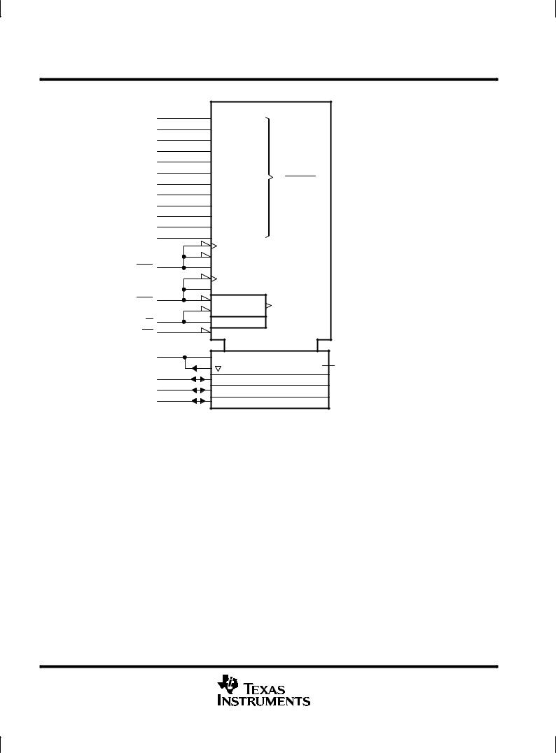
functional block diagram
TMS416409A, TMS426409A |
|
|
|
|
|
|
|
||
|
|
|
RAS |
CAS |
W |
OE |
|
|
|
|
|
|
|
Timing and Control |
|
|
|||
A0 |
|
10 |
|
Column Decode |
|
|
|
||
A1 |
|
|
|
|
|
||||
|
|
|
|
|
|
|
|
|
|
|
Column- |
|
|
Sense Amplifiers |
4 |
|
|
||
|
Address |
|
R |
|
256K Array |
|
Data- |
|
|
|
Buffers² |
|
|
|
|
||||
|
|
o |
|
256K Array |
|
In |
4 |
||
A11 |
|
|
|
|
|||||
|
|
w |
|
|
|
4 |
Reg. |
|
|
|
|
|
|
|
|
|
|||
|
|
|
|
|
|
|
I/O |
|
4 |
|
|
|
D |
|
|
|
Buffers |
|
|
|
Row- |
|
e |
|
|
|
64 |
Data- |
|
|
|
|
|
|
|
|
|||
|
|
c |
|
|
|
|
Out |
|
|
|
Address |
12 |
|
|
|
|
|
||
|
o |
|
|
|
|
Reg. |
|
||
|
Buffers |
|
|
|
|
|
|||
|
|
|
|
|
|
|
|||
|
|
d |
|
|
|
|
|
|
|
|
|
|
|
|
|
|
|
|
|
|
|
|
e |
|
256K Array |
|
|
DQ1 ± DQ4 |
|
|
|
|
|
|
|
|
|
|
|
|
|
|
12 |
|
|
|
|
|
|
² Column addresses A10 and A11 are not used.
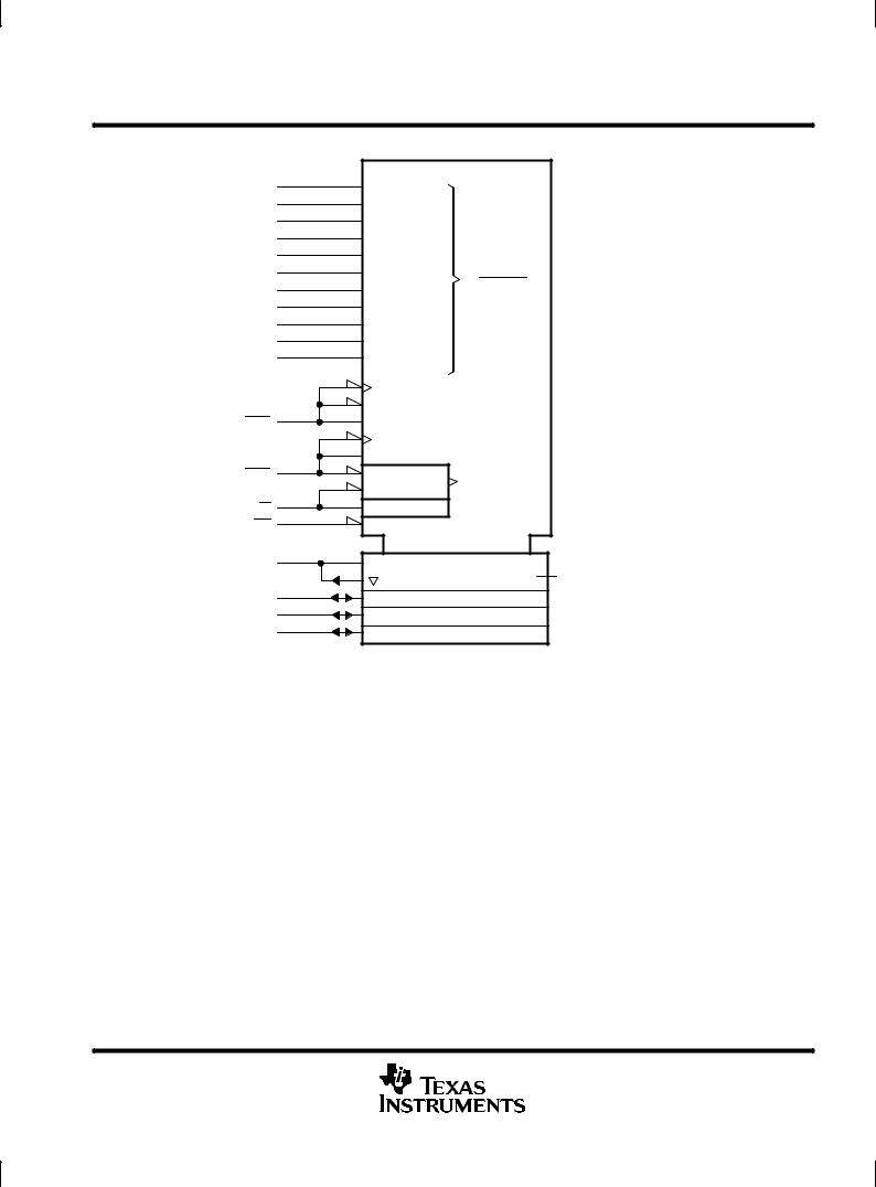
TMS417409A, TMS427409A |
|
|
|
|
|
|
|
||
|
|
|
RAS |
CAS |
W |
OE |
|
|
|
|
|
|
Timing and Control |
|
|
||||
A0 |
|
11 |
Column Decode |
|
|
|
|||
A1 |
|
|
|
|
|||||
|
|
|
|
|
|
|
|
|
|
|
Column- |
|
Sense Amplifiers |
4 |
|
|
|||
|
Address |
|
256K Array |
R |
256K Array |
Data- |
|
||
|
Buffers |
|
|
||||||
|
|
256K Array |
o |
256K Array |
In |
4 |
|||
A10 |
|
|
|||||||
|
|
|
|
w |
|
4 |
Reg. |
|
|
|
|
|
|
|
|
|
|||
|
|
|
|
|
|
|
I/O |
|
4 |
|
|
|
32 |
|
D |
|
Buffers |
|
|
|
Row- |
|
|
e |
|
32 |
Data- |
|
|
|
|
|
|
|
|
|
|||
|
|
|
|
c |
|
|
Out |
|
|
|
Address |
11 |
|
|
|
|
|
||
|
|
|
o |
|
|
Reg. |
|
||
|
Buffers |
|
|
|
|
|
|||
|
|
|
|
|
|
|
|||
|
|
|
|
d |
|
|
|
|
|
|
|
|
|
|
|
|
|
|
|
|
|
|
256K Array |
e |
256K Array |
|
DQ1 ± DQ4 |
||
|
|
|
|
|
|
|
|
|
|
|
|
|
11 |
|
|
|
|
|
|
4 |
POST OFFICE BOX 1443 •HOUSTON, TEXAS 77251±1443 |
TMS416409A, TMS417409A, TMS426409A, TMS427409A 4194304 BY 4-BIT EXTENDED DATA OUT DYNAMIC RANDOM-ACCESS MEMORIES
SMKS893B ± AUGUST 1996 ± REVISED APRIL 1997
operation
extended data out
Extended data out (EDO) allows data output rates of up to 50 MHz for 50-ns devices. When keeping the same row address while selecting random column addresses, the time for row-address setup and hold and for address multiplex is eliminated. The maximum number of columns that can be accessed is determined by tRASP , the
maximum RAS low time.
Extended data out does not place the data in/data out pins (DQ pins) into the high-impedance state with the rising edge of CAS. The output remains valid for the system to latch the data. After CAS goes high, the DRAM decodes the next address. OE and W can control the output impedance. Descriptions of OE and W further explain EDO operation benefit.
address: A0±A11 (TMS416409A and TMS426409A) and A0±A10 (TMS417409A and TMS427409A)
Twenty-two address bits are required to decode each of the 4194304 storage cell locations. For the TMS416409A and TMS426409A,12 row-address bits are set up on A0 through A11 and latched onto the chip by the row-address strobe (RAS). Ten column-address bits are set up on A0 through A9. For the TMS417409A and TMS427409A, 11 row-address bits are set up on inputs A0 through A10 and latched onto the chip by RAS. Eleven column-address bits are set up on A0 through A10. All addresses must be stable on or before the falling edge of RAS and CAS. RAS is similar to a chip enable because it activates the sense amplifiers as well as the row decoder. CAS is used as a chip select, activating the output buffers and latching the address bits into the column-address buffers.
output enable (OE)
OE controls the impedance of the output buffers. While CAS and RAS are low and W is high, OE can be brought low or high and the DQs transition between valid data and high impedance (see Figure 8). There are two methods for placing the DQs into the high-impedance state and maintaining that state during CAS high time. The first method is to transition OE high before CAS transitions high and keep OE high for tCHO (hold time, OE
from CAS) past the CAS transition. This disables the DQs and they remain disabled, regardless of OE, until CAS falls again. The second method is to have OE low as CAS transitions high. Then OE can pulse high for a minimum of tOEP (precharge time, OE) anytime during CAS high time, disabling the DQs regardless of further
transitions on OE until CAS falls again (see Figure 8).
write enable (W )
The read or write mode is selected through W. A logic high on W selects the read mode, and a logic low selects the write mode. The data inputs are disabled when the read mode is selected. When W goes low prior to CAS (early write), data out remains in the high-impedance state for the entire cycle, permitting a write operation with OE grounded. If W goes low in an extended-data-out read cycle, the DQs are disabled so long as CAS is high (see Figure 9).
data in/data out (DQ1±DQ4)
Data is written during a write or read-modify-write cycle. Depending on the mode of operation, the later falling edge of CAS or W strobes data into the on-chip data latch with setup and hold times referenced to the later edge. The DQs drive valid data after all access times are met and remain valid except in cases described in the W and OE sections.
POST OFFICE BOX 1443 •HOUSTON, TEXAS 77251±1443 |
5 |
TMS416409A, TMS417409A, TMS426409A, TMS427409A 4194304 BY 4-BIT EXTENDED DATA OUT
DYNAMIC RANDOM-ACCESS MEMORIES
SMKS893B ± AUGUST 1996 ± REVISED APRIL 1997
RAS-only refresh
TMS416409A, TMS426409A
A refresh operation must be performed at least once every 64 ms to retain data. This can be achieved by strobing each of the 4096 rows (A0±A11). A normal read or write cycle refreshes all bits in each row that is selected. A RAS-only operation can be used by holding CAS at the high (inactive) level, conserving power as the output buffers remain in the high-impedance state. Externally generated addresses must be used for a RAS-only refresh.
TMS417409A, TMS427409A
A refresh operation must be performed at least once every 32 ms to retain data. This can be achieved by strobing each of the 2048 rows (A0±A10). A normal read or write cycle refreshes all bits in each row that is selected. A RAS-only operation can be used by holding CAS at the high (inactive) level, conserving power as the output buffers remain in the high-impedance state. Externally generated addresses must be used for a RAS-only refresh.
hidden refresh
A hidden refresh can be performed while maintaining valid data at the output pin. This is accomplished by holding CAS at VIL after a read operation and cycling RAS after a specified precharge period, similar to a RAS-only refresh cycle. The external address is ignored, and the refresh address is generated internally.
CAS-before-RAS (CBR) refresh
CBR refresh is performed by bringing CAS low earlier than RAS (see parameter tCSR) and holding it low after
RAS falls (see parameter tCHR). For successive CBR refresh cycles, CAS can remain low while cycling RAS. The external address is ignored, and the refresh address is generated internally.
power up
To achieve proper device operation, an initial pause of 200 ms followed by a minimum of eight initialization cycles is required after power up to the full VCC level. These eight initialization cycles must include at least one refresh
(RAS-only or CBR) cycle.
test mode
The test mode (see Figure 1) is initiated with a CBR-refresh cycle while simultaneously holding the W input low. The entry cycle performs an internal refresh cycle while internally setting the device to perform parallel read or write on subsequent cycles. While in the test mode, any data sequence can be performed. The device exits test mode if a CBR refresh cycle with W held high or a RAS-only refresh cycle is performed.
In the test mode, the device is configured as 1024K bits ×4 bits for each DQ. Each DQ pin has a separate 4-bit parallel read and write data bus that ignores column addresses A0 and A1. During a read cycle, the four internal bits are compared for each DQ pin. If the four bits agree, DQ goes high; if not, DQ goes low. Test time is reduced by a factor of four for this series.
6 |
POST OFFICE BOX 1443 •HOUSTON, TEXAS 77251±1443 |
|
TMS416409A, TMS417409A, TMS426409A, TMS427409A |
||
|
|
4194304 BY 4-BIT EXTENDED DATA OUT |
|
|
|
DYNAMIC RANDOM-ACCESS MEMORIES |
|
|
|
SMKS893B ± AUGUST 1996 ± REVISED APRIL 1997 |
|
test mode (continued) |
|
|
|
|
|
Exit Cycle |
|
Entry Cycle |
Test Mode Cycle |
Normal |
|
Mode |
|||
|
|
||
RAS
CAS
W
NOTE A: The states of W, data in, and address are defined by the type of cycle used during test mode.
Figure 1. Test-Mode Cycle
POST OFFICE BOX 1443 •HOUSTON, TEXAS 77251±1443 |
7 |
TMS416409A, TMS417409A, TMS426409A, TMS427409A 4194304 BY 4-BIT EXTENDED DATA OUT
DYNAMIC RANDOM-ACCESS MEMORIES
SMKS893B ± AUGUST 1996 ± REVISED APRIL 1997
absolute maximum ratings over operating free-air temperature range (unless otherwise noted)²
Supply voltage range, VCC (TMS41x409A) . . . . . . . . . . . . . . . . . . . . . . . . . . . . . . . . . . . . . . . . . . |
. . . . ± 1 V to 7 |
V |
Supply voltage range, VCC (TMS42x409A) . . . . . . . . . . . . . . . . . . . . . . . . . . . . . . . . . . . . . . . . . . |
± 0.5 V to 4.6 |
V |
Voltage range on any pin (TMS41x409A) (see Note 1) . . . . . . . . . . . . . . . . . . . . . . . . . . . . . . . . . |
. . . ± 1 V to 7 |
V |
Voltage range on any pin (TMS42x409A) (see Note 1) . . . . . . . . . . . . . . . . . . . . . . . . . . . . . . . . |
± 0.5 V to 4.6 |
V |
Short-circuit output current . . . . . . . . . . . . . . . . . . . . . . . . . . . . . . . . . . . . . . . . . . . . . . . . . . . . . . . . . |
. . . . . . . 50 mA |
|
Power dissipation . . . . . . . . . . . . . . . . . . . . . . . . . . . . . . . . . . . . . . . . . . . . . . . . . . . . . . . . . . . . . . . . . |
. . . . . . . . . 1 W |
|
Operating free-air temperature range, TA . . . . . . . . . . . . . . . . . . . . . . . . . . . . . . . . . . . . . . . . . . . . |
. . 0°C to 70°C |
|
Storage temperature range, Tstg . . . . . . . . . . . . . . . . . . . . . . . . . . . . . . . . . . . . . . . . . . . . . . . . . . |
± 55°C to 125°C |
|
²Stresses beyond those listed under ªabsolute maximum ratingsº may cause permanent damage to the device. These are stress ratings only, and functional operation of the device at these or any other conditions beyond those indicated under ªrecommended operating conditionsº is not implied. Exposure to absolute-maximum-rated conditions for extended periods may affect device reliability.
NOTE 1: All voltage values are with respect to VSS.
recommended operating conditions
|
|
TMS41x409A |
|
TMS42x409A |
|
|||
|
|
|
|
|
|
|
|
|
|
|
MIN |
NOM |
MAX |
MIN |
NOM |
MAX |
UNIT |
|
|
|
|
|
|
|
|
|
VCC |
Supply voltage |
4.5 |
5 |
5.5 |
3 |
3.3 |
3.6 |
V |
VSS |
Supply voltage |
|
0 |
|
|
0 |
|
V |
VIH |
High-level input voltage |
2.4 |
|
6.5 |
2 |
|
VCC + 0.3 |
V |
VIL |
Low-level input voltage (see Note 2) |
± 1 |
|
0.8 |
± 0.3 |
|
0.8 |
V |
TA |
Operating free-air temperature |
0 |
|
70 |
0 |
|
70 |
°C |
NOTE 2: The algebraic convention, where the more negative (less positive) limit is designated as minimum, is used for logic-voltage levels only.
8 |
POST OFFICE BOX 1443 •HOUSTON, TEXAS 77251±1443 |
TMS416409A, TMS417409A, TMS426409A, TMS427409A 4194304 BY 4-BIT EXTENDED DATA OUT DYNAMIC RANDOM-ACCESS MEMORIES
SMKS893B ± AUGUST 1996 ± REVISED APRIL 1997
electrical characteristics over recommended ranges of supply voltage and operating free-air temperature (unless otherwise noted)
TMS416409A
|
PARAMETER |
TEST CONDITIONS² |
'416409A - 50 |
'416409A - 60 |
'416409 A- 70 |
UNIT |
||||
|
|
|
|
|
||||||
|
MIN |
MAX |
MIN MAX |
MIN MAX |
||||||
|
|
|
|
|
|
|
||||
|
|
|
|
|
|
|
|
|
|
|
VOH |
High-level output |
IOH = ± 5 mA |
|
2.4 |
|
2.4 |
2.4 |
V |
||
voltage |
|
|
||||||||
|
|
|
|
|
|
|
|
|
|
|
|
|
|
|
|
|
|
|
|
|
|
VOL |
Low-level output voltage |
IOL = 4.2 mA |
|
|
0.4 |
0.4 |
0.4 |
V |
||
II |
Input current (leakage) |
VCC = 5.5 V, |
VI = 0 V to 6.5 V, |
|
± 10 |
± 10 |
± 10 |
μA |
||
All others = 0 V to VCC |
|
|||||||||
|
|
|
|
|
|
|
||||
IO |
Output current |
VCC = 5.5 V, |
VO = 0 V to VCC, |
|
± 10 |
± 10 |
± 10 |
μA |
||
(leakage) |
CAS high |
|
|
|||||||
|
|
|
|
|
|
|
||||
|
|
|
|
|
|
|
|
|
|
|
ICC1³§ |
Average reador |
VCC = 5.5 V, |
Minimum cycle |
|
100 |
80 |
70 |
mA |
||
write-cycle current |
|
|||||||||
|
|
|
|
|
|
|
|
|
|
|
|
|
|
|
|
|
|
|
|
|
|
|
|
VIH = 2.4 V ( TTL), |
|
|
|
|
|
|
||
|
|
After one memory cycle, |
|
2 |
2 |
2 |
mA |
|||
ICC2 |
Average standby |
RAS and CAS high |
|
|
|
|
|
|
||
current |
VIH = VCC ± 0.2 V (CMOS), |
|
|
|
|
|
||||
|
|
After one memory cycle, |
|
1 |
1 |
1 |
mA |
|||
|
|
RAS and CAS high |
|
|
|
|
|
|
||
|
|
|
|
|
|
|
|
|
||
|
Average refresh current |
VCC = 5.5 V, |
Minimum cycle, |
|
|
|
|
|
||
ICC3³§ |
RAS cycling, |
|
|
|
|
|
|
|||
(RAS-only refresh or |
|
|
100 |
80 |
70 |
mA |
||||
|
|
|
|
|
||||||
CAS high (RAS only), |
|
|||||||||
|
CBR) |
|
|
|
|
|
||||
|
RAS low after CAS low (CBR) |
|
|
|
|
|
||||
|
|
|
|
|
|
|
||||
|
|
|
|
|
|
|
|
|
||
ICC4³¶ |
Average EDO current |
VCC = 5.5 V, |
tHPC = MIN, |
|
100 |
90 |
80 |
mA |
||
RAS low, |
CAS cycling |
|
||||||||
|
|
|
|
|
|
|
||||
² For conditions shown as MIN / MAX, use the appropriate value specified in the timing requirements. ³ Measured with outputs open
§ Measured with a maximum of one address change while RAS = VIL
¶ Measured with a maximum of one address change during each EDO cycle, tHPC
POST OFFICE BOX 1443 •HOUSTON, TEXAS 77251±1443 |
9 |

TMS416409A, TMS417409A, TMS426409A, TMS427409A 4194304 BY 4-BIT EXTENDED DATA OUT
DYNAMIC RANDOM-ACCESS MEMORIES
SMKS893B ± AUGUST 1996 ± REVISED APRIL 1997
electrical characteristics over recommended ranges of supply voltage and operating free-air temperature (unless otherwise noted) (continued)
TMS417409A
|
PARAMETER |
TEST CONDITIONS² |
'417409 A- 50 |
'417409A - 60 |
'417409A - 70 |
UNIT |
|||
|
|
|
|
|
|||||
|
MIN |
MAX |
MIN MAX |
MIN MAX |
|||||
|
|
|
|
|
|
||||
|
|
|
|
|
|
|
|
|
|
VOH |
High-level output |
IOH = ± 5 mA |
|
|
2.4 |
|
2.4 |
2.4 |
V |
voltage |
|
|
|
||||||
|
|
|
|
|
|
|
|
|
|
|
|
|
|
|
|
|
|
|
|
VOL |
Low-level output voltage |
IOL = 4.2 mA |
|
|
|
0.4 |
0.4 |
0.4 |
V |
II |
Input current (leakage) |
VCC = 5.5 V, |
VI = 0 V to 6.5 V, |
|
± 10 |
± 10 |
± 10 |
μA |
|
All others = 0 V to VCC |
|
||||||||
|
|
|
|
|
|
|
|||
IO |
Output current |
VCC = 5.5 V, |
VO = 0 V to VCC, |
|
± 10 |
± 10 |
± 10 |
μA |
|
(leakage) |
CAS high |
|
|
|
|||||
|
|
|
|
|
|
|
|
||
|
|
|
|
|
|
|
|
|
|
ICC1³§ |
Average reador |
VCC = 5.5 V, |
Minimum cycle |
|
130 |
110 |
100 |
mA |
|
write-cycle current |
|
||||||||
|
|
|
|
|
|
|
|
|
|
|
|
|
|
|
|
|
|
|
|
|
|
VIH = 2.4 V ( TTL), |
|
|
|
|
|
||
|
|
After one memory cycle, |
|
2 |
2 |
2 |
mA |
||
ICC2 |
Average standby |
RAS and CAS high |
|
|
|
|
|
||
current |
VIH = VCC ± 0.2 V (CMOS), |
|
|
|
|
|
|||
|
|
After one memory cycle, |
|
1 |
1 |
1 |
mA |
||
|
|
RAS and CAS high |
|
|
|
|
|
||
|
|
|
|
|
|
|
|
|
|
ICC3³§ |
Average refresh current |
VCC = 5.5 V, |
Minimum cycle, |
|
|
|
|
|
|
(RAS-only refresh or |
RAS cycling, |
CAS high (RAS only), |
|
130 |
110 |
100 |
mA |
||
|
CBR) |
RAS low after |
CAS |
low (CBR) |
|
|
|
|
|
|
|
|
|
|
|
|
|
|
|
ICC4³¶ |
Average EDO current |
VCC = 5.5 V, |
tHPC = MIN, |
|
110 |
90 |
80 |
mA |
|
RAS low, |
CAS cycling |
|
|||||||
|
|
|
|
|
|
|
|||
² For conditions shown as MIN / MAX, use the appropriate value specified in the timing requirements. ³ Measured with outputs open
§ Measured with a maximum of one address change while RAS = VIL
¶ Measured with a maximum of one address change during each EDO cycle, tHPC
10 |
POST OFFICE BOX 1443 •HOUSTON, TEXAS 77251±1443 |
TMS416409A, TMS417409A, TMS426409A, TMS427409A 4194304 BY 4-BIT EXTENDED DATA OUT DYNAMIC RANDOM-ACCESS MEMORIES
SMKS893B ± AUGUST 1996 ± REVISED APRIL 1997
electrical characteristics over recommended ranges of supply voltage and operating free-air temperature (unless otherwise noted) (continued)
TMS426409A
PARAMETER |
TEST CONDITIONS² |
'426409A - 50 |
'426409A -60 |
'426409A - 70 |
UNIT |
|||||||||||||
|
|
|
|
|
|
|||||||||||||
MIN |
MAX |
MIN |
MAX |
MIN |
MAX |
|||||||||||||
|
|
|
|
|
|
|
|
|
|
|
|
|||||||
|
|
|
|
|
|
|
|
|
|
|
|
|
|
|
|
|
|
|
VOH |
High-level |
IOH = ± 2 mA |
|
|
|
LVTTL |
2.4 |
|
2.4 |
|
2.4 |
|
V |
|||||
output |
|
|
|
|
|
|
|
|
|
|
|
|
|
|
|
|||
IOH = ± 100 μA |
|
|
|
LVCMOS |
VCC ± 0.2 |
|
VCC ± 0.2 |
|
VCC ± 0.2 |
|
||||||||
|
voltage |
|
|
|
|
|
|
|
||||||||||
VOL |
Low-level |
IOL = 2 mA |
|
|
|
LVTTL |
|
0.4 |
|
0.4 |
|
0.4 |
V |
|||||
output |
|
|
|
|
|
|
|
|
|
|
|
|
|
|
|
|||
IOL = 100 μA |
|
|
|
LVCMOS |
|
0.2 |
|
0.2 |
|
0.2 |
||||||||
|
voltage |
|
|
|
|
|
|
|
||||||||||
II |
Input current |
VCC = 3.6 V, |
VI = 0 V to 3.9 V, |
|
± 10 |
|
± 10 |
|
± 10 |
μA |
||||||||
(leakage) |
All others = 0 V to VCC |
|
|
|
||||||||||||||
|
|
|
|
|
|
|
|
|||||||||||
|
Output |
VCC = 3.6 V, |
VO = 0 V to VCC, |
|
|
|
|
|
|
|
||||||||
IO |
current |
|
± 10 |
|
± 10 |
|
± 10 |
μA |
||||||||||
CAS high |
|
|
|
|
|
|
|
|
|
|||||||||
|
(leakage) |
|
|
|
|
|
|
|
|
|
|
|
|
|
||||
|
|
|
|
|
|
|
|
|
|
|
|
|
|
|
|
|
||
|
|
|
|
|
|
|
|
|
|
|
|
|
|
|
|
|
|
|
|
Average |
|
|
|
|
|
|
|
|
|
|
|
|
|
|
|
|
|
ICC1³§ |
reador |
VCC = 3.6 V, |
Minimum cycle |
|
90 |
|
70 |
|
60 |
mA |
||||||||
writecycle |
|
|
|
|||||||||||||||
|
|
|
|
|
|
|
|
|
|
|
|
|
|
|
|
|
||
|
current |
|
|
|
|
|
|
|
|
|
|
|
|
|
|
|
|
|
|
|
|
|
|
|
|
|
|
|
|
|
|
|
|
|
|
|
|
|
|
VIH = 2 V (LVTTL) |
|
|
|
|
|
|
|
|
|
|
|
|
|
|||
|
Average |
After one memory cycle, |
RAS |
and |
CAS |
|
|
2 |
|
2 |
|
2 |
mA |
|||||
|
high |
|
|
|
|
|
|
|
|
|
|
|
|
|
||||
ICC2 |
standby |
|
|
|
|
|
|
|
|
|
|
|
|
|
||||
|
|
|
|
|
|
|
|
|
|
|
|
|
|
|
|
|||
VIH = VCC ± 0.2 V (LVCMOS), |
|
|
|
|
|
|
|
|
|
|||||||||
|
current |
|
|
|
1 |
|
1 |
|
1 |
mA |
||||||||
|
|
After one memory cycle, RAS and CAS |
|
|
|
|||||||||||||
|
|
high |
|
|
|
|
|
|
|
|
|
|
|
|
|
|||
|
|
|
|
|
|
|
|
|
|
|
|
|
|
|
|
|
|
|
|
Average |
|
|
|
|
|
|
|
|
|
|
|
|
|
|
|
|
|
|
refresh |
VCC = 3.6 V, |
Minimum cycle, |
|
|
|
|
|
|
|
||||||||
ICC3³§ |
current |
RAS cycling, |
|
|
|
|
|
|
|
90 |
|
70 |
|
60 |
mA |
|||
(RAS-only |
|
|
|
|
|
|
|
|
|
|
|
|
||||||
CAS high (RAS-only refresh), |
|
|
|
|||||||||||||||
|
|
|
|
|
|
|
|
|||||||||||
|
refresh |
RAS low after CAS low (CBR) |
|
|
|
|
|
|
|
|||||||||
|
or CBR) |
|
|
|
|
|
|
|
|
|
|
|
|
|
|
|
|
|
|
|
|
|
|
|
|
|
|
|
|
||||||||
ICC4³¶ |
Average |
VCC = 3.6 V, |
tHPC = MIN, |
|
100 |
|
90 |
|
80 |
mA |
||||||||
EDO current |
RAS low, |
CAS cycling |
|
|
|
|||||||||||||
|
|
|
|
|
|
|
|
|||||||||||
² For conditions shown as MIN / MAX, use the appropriate value specified in the timing requirements. ³ Measured with outputs open
§ Measured with a maximum of one address change while RAS = VIL
¶ Measured with a maximum of one address change during each EDO cycle, tHPC
POST OFFICE BOX 1443 •HOUSTON, TEXAS 77251±1443 |
11 |

TMS416409A, TMS417409A, TMS426409A, TMS427409A 4194304 BY 4-BIT EXTENDED DATA OUT
DYNAMIC RANDOM-ACCESS MEMORIES
SMKS893B ± AUGUST 1996 ± REVISED APRIL 1997
electrical characteristics over recommended ranges of supply voltage and operating free-air temperature (unless otherwise noted) (continued)
TMS427409A
PARAMETER |
TEST CONDITIONS² |
'427409A - 50 |
'427409A -60 |
'427409A - 70 |
UNIT |
|||||||||||||
|
|
|
|
|
|
|||||||||||||
MIN |
MAX |
MIN |
MAX |
MIN |
MAX |
|||||||||||||
|
|
|
|
|
|
|
|
|
|
|
|
|||||||
|
|
|
|
|
|
|
|
|
|
|
|
|
|
|
|
|
|
|
VOH |
High-level |
IOH = ± 2 mA |
|
|
LVTTL |
2.4 |
|
2.4 |
|
2.4 |
|
V |
||||||
output |
|
|
|
|
|
|
|
|
|
|
|
|
|
|
|
|||
IOH = ± 100 μA |
|
|
LVCMOS |
VCC ± 0.2 |
|
VCC ± 0.2 |
|
VCC ± 0.2 |
|
|||||||||
|
voltage |
|
|
|
|
|
|
|||||||||||
VOL |
Low-level |
IOL = 2 mA |
|
|
LVTTL |
|
0.4 |
|
0.4 |
|
0.4 |
V |
||||||
output |
|
|
|
|
|
|
|
|
|
|
|
|
|
|
|
|||
IOL = 100 μA |
|
|
LVCMOS |
|
0.2 |
|
0.2 |
|
0.2 |
|||||||||
|
voltage |
|
|
|
|
|
|
|||||||||||
II |
Input current |
VCC = 3.6 V, |
VI = 0 V to 3.9 V, |
|
± 10 |
|
± 10 |
|
± 10 |
μA |
||||||||
(leakage) |
All others = 0 V to VCC |
|
|
|
||||||||||||||
|
|
|
|
|
|
|
|
|||||||||||
|
Output |
VCC = 3.6 V, |
VO = 0 V to VCC, |
|
|
|
|
|
|
|
||||||||
IO |
current |
|
± 10 |
|
± 10 |
|
± 10 |
μA |
||||||||||
CAS high |
|
|
|
|
|
|
|
|
|
|||||||||
|
(leakage) |
|
|
|
|
|
|
|
|
|
|
|
|
|
||||
|
|
|
|
|
|
|
|
|
|
|
|
|
|
|
|
|
||
|
|
|
|
|
|
|
|
|
|
|
|
|
|
|
|
|
|
|
|
Average |
|
|
|
|
|
|
|
|
|
|
|
|
|
|
|
|
|
ICC1³§ |
reador |
VCC = 3.6 V, |
Minimum cycle |
|
120 |
|
100 |
|
90 |
mA |
||||||||
writecycle |
|
|
|
|||||||||||||||
|
|
|
|
|
|
|
|
|
|
|
|
|
|
|
|
|
||
|
current |
|
|
|
|
|
|
|
|
|
|
|
|
|
|
|
|
|
|
|
|
|
|
|
|
|
|
|
|
|
|
|
|
|
|
|
|
|
|
VIH = 2 V (LVTTL) |
|
|
|
|
|
|
|
|
|
|
|
|
|
|||
|
Average |
After one memory cycle, |
RAS |
and |
CAS |
|
|
2 |
|
2 |
|
2 |
mA |
|||||
|
high |
|
|
|
|
|
|
|
|
|
|
|
|
|
||||
ICC2 |
standby |
|
|
|
|
|
|
|
|
|
|
|
|
|
||||
|
|
|
|
|
|
|
|
|
|
|
|
|
|
|
|
|||
VIH = VCC ± 0.2 V (LVCMOS), |
|
|
|
|
|
|
|
|
|
|||||||||
|
current |
|
|
|
1 |
|
1 |
|
1 |
mA |
||||||||
|
|
After one memory cycle, RAS and CAS |
|
|
|
|||||||||||||
|
|
high |
|
|
|
|
|
|
|
|
|
|
|
|
|
|||
|
|
|
|
|
|
|
|
|
|
|
|
|
|
|
|
|
|
|
|
Average |
|
|
|
|
|
|
|
|
|
|
|
|
|
|
|
|
|
|
refresh |
VCC = 3.6 V, |
Minimum cycle, |
|
|
|
|
|
|
|
||||||||
ICC3³§ |
current |
RAS cycling, |
|
|
|
|
|
|
|
120 |
|
100 |
|
90 |
mA |
|||
(RAS-only |
|
|
|
|
|
|
|
|
|
|
|
|
||||||
CAS high (RAS-only refresh), |
|
|
|
|||||||||||||||
|
|
|
|
|
|
|
|
|||||||||||
|
refresh |
RAS low after CAS low (CBR) |
|
|
|
|
|
|
|
|||||||||
|
or CBR) |
|
|
|
|
|
|
|
|
|
|
|
|
|
|
|
|
|
|
|
|
|
|
|
|
|
|
|
|
||||||||
ICC4³¶ |
Average |
VCC = 3.6 V, |
tHPC = MIN, |
|
110 |
|
90 |
|
80 |
mA |
||||||||
EDO current |
RAS low, |
CAS cycling |
|
|
|
|||||||||||||
|
|
|
|
|
|
|
|
|||||||||||
² For conditions shown as MIN / MAX, use the appropriate value specified in the timing requirements. ³ Measured with outputs open
§ Measured with a maximum of one address change while RAS = VIL
¶ Measured with a maximum of one address change during each EDO cycle, tHPC
12 |
POST OFFICE BOX 1443 •HOUSTON, TEXAS 77251±1443 |
 Loading...