


LM70
July 2000
LM70
SPI/MICROWIRE™ 10-Bit plus Sign Digital Temperature Sensor
General Description
The LM70 is a temperature sensor, Delta-Sigma analog-to-digital converter with an SPI and MICROWIRE compatible interface available in LLP and MSOP 8-pin packages. The host can query the LM70 at any time to read temperature. A shutdown mode decreases power consumption to less than 10 µA. This mode is useful in systems where low average power consumption is critical.
The LM70 has 10-bit plus sign temperature resolution (0.25ÊC per LSB) while operating over a temperature range of −55ÊC to +150ÊC.
The LM70's 2.65V to 5.5V supply voltage range, low supply current and simple SPI interface make it ideal for a wide range of applications. These include thermal management and protection applications in hard disk drives, printers, electronic test equipment, and office electronics.
Applications
nSystem Thermal Management
nPersonal Computers
nDisk Drives
nOffice Electronics
n Electronic Test Equipment
Features
n0.25ÊC temperature resolution.
nShutdown mode conserves power between temperature reading
nSPI and MICROWIRE Bus interface
nMSOP-8 and LLP-8 packages save space
Key Specifications
j Supply Voltage |
|
2.65V to 5.5V |
j Supply Current |
operating |
260µA (typ) |
|
|
490µA (max) |
|
shutdown |
12µA (typ) |
j Temperature |
−40ÊC to 85ÊC |
±2ÊC(max) |
Accuracy |
−10ÊC to 65ÊC |
+1.5/−2ÊC(max) |
|
−55ÊC to 125ÊC |
+3/−2ÊC(max) |
|
−55ÊC to 150ÊC |
+3.5/−2ÊC(max) |
Simplified Block Diagram
DS101223-1
MICROWIRE® is a registered trademark of National Semiconductor Corporation.
Sensor Temperature Digital Sign plus Bit-SPI/MICROWIRE10 LM70
© 2000 National Semiconductor Corporation |
DS101223 |
www.national.com |
LM70
Connection Diagrams
MSOP-8 |
LLP-8 |
DS101223-2 |
|
TOP VIEW |
DS101223-25 |
|
|
NS Package Number MUA08A |
TOP VIEW |
|
NS Package Number LDA08A |
Ordering Information
Order Number |
Package |
NS Package |
Supply Voltage |
Transport Media |
|
Marking |
Number |
||||
|
|
|
|||
|
|
|
|
|
|
LM70CILD-3 |
T33 |
LLP-8, LDA08A |
2.65V to 3.6V |
_ Units in Rail |
|
|
|
|
|
|
|
LM70CILDX-3 |
T33 |
LLP-8, LDA08A |
2.65V to 3.6V |
_ Units in Rail |
|
|
|
|
|
|
|
LM70CILD-5 |
T35 |
LLP-8, LDA08A |
4.5V to 5.5V |
_ Units in Tape and Reel |
|
|
|
|
|
|
|
LM70CILDX-5 |
T35 |
LLP-8, LDA08A |
4.5V to 5.5V |
_ Units in Tape and Reel |
|
|
|
|
|
|
|
LM70CIMM-3 |
T04C |
MSOP-8, MUA08A |
2.65V to 3.6V |
250 Units in Rail |
|
|
|
|
|
|
|
LM70CIMMX-3 |
T04C |
MSOP-8, MUA08A |
2.65V to 3.6V |
3500 Units in Tape and Reel |
|
|
|
|
|
|
|
LM70CIMM-5 |
T03C |
MSOP-8, MUA08A |
4.5V to 5.5V |
250 Units in Rail |
|
|
|
|
|
|
|
LM70CIMMX-5 |
T03C |
MSOP-8, MUA08A |
4.5V to 5.5V |
3500 Units in Tape and Reel |
|
|
|
|
|
|
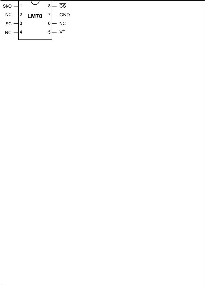
Pin Descriptions
|
Label |
SOP-8 |
LLP-8 |
Function |
Typical Connection |
|
|
|
|
Pin # |
Pin # |
|
|
|
|
|
|
|
|
|
|
SI/O |
1 |
1 |
Input/Output - Serial bus bi-directional data |
From and to Controller |
|
|
|
|
|
|
line. Schmitt trigger input. |
|
|
|
|
|
|
|
|
|
SC |
2 |
3 |
Clock - Serial bus clock Schmitt trigger input |
From Controller |
|
|
|
|
|
|
line. |
|
|
|
|
|
|
|
|
|
GND |
4 |
7 |
Power Supply Ground |
Ground |
|
|
|
|
|
|
|
|
|
V+ |
5 |
5 |
Positive Supply Voltage Input |
DC Voltage from 2.65V to 5.5V. Bypass |
|
|
|
|
|
|
|
with a 0.1 µF ceramic capacitor. |
|
|
|
|
|
|
|
|
|
7 |
8 |
Chip Select input. |
From Controller |
|
|
CS |
|
||||
|
|
|
|
|
|
|
|
NC |
3, 6, 8 |
2, 4, 6 |
No Connect |
These pins are not connected to the |
|
|
|
|
|
|
|
LM70 die in any way. |
|
|
|
|
|
|
|
www.national.com |
2 |
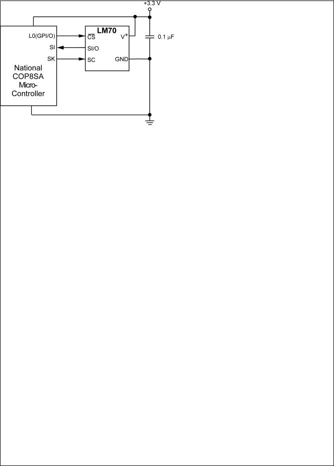
Typical Application
DS101223-3
FIGURE 1. COP Microcontroller Interface
LM70
3 |
www.national.com |

LM70
Absolute Maximum Ratings (Note 1)
Supply Voltage |
−0.3V to 6.0V |
Voltage at any Pin |
−0.3V to V + + 0.3V |
Input Current at any Pin (Note 2) |
5 mA |
Package Input Current (Note 2) |
20 mA |
Storage Temperature |
−65ÊC to +150ÊC |
Soldering Information, Lead Temperature |
|
MSOP-8 and LLP-8 Packages |
|
(Note 3) |
|
Vapor Phase (60 seconds) |
215ÊC |
Infrared (15 seconds) |
220ÊC |
ESD Susceptibility (Note 4) |
|
Human Body Model |
3000V |
Machine Model |
300V |
Operating Ratings
Specified Temperature Range |
TMIN to TMAX |
(Note 5) |
−55ÊC to +150ÊC |
Supply Voltage Range (+VS) |
+2.65V to +5.5V |
Temperature-to-Digital Converter Characteristics
Unless otherwise noted, these specifications apply for V+ = 2.65V to 3.6V for the LM70-3 and V+ = 4.5V to 5.5V for the LM70-5 (Note 6). Boldface limits apply for TA = TJ = TMIN to TMAX; all other limits TA = TJ=+25ÊC, unless otherwise noted.
|
|
Typical |
LM70-5 |
LM70-3 |
Units |
Parameter |
Conditions |
(Note 7) |
Limits |
Limits |
(Limit) |
|
|
|
(Note 8) |
(Note 8) |
|
|
|
|
|
|
|
Temperature Error (Note 6) |
TA = −10ÊC to +65ÊC |
|
+1.5/−2.0 |
+1.5/−2.0 |
ÊC (max) |
|
TA = −40ÊC to +85ÊC |
|
± 2.0 |
± 2.0 |
ÊC (max) |
|
TA = −55ÊC to +125ÊC |
|
+3.0/−2.0 |
+3.0/−2.0 |
ÊC (max) |
|
TA = −55ÊC to +150ÊC |
|
+3.5/−2.0 |
+3.5/−2.0 |
ÊC (max) |
Resolution |
|
11 |
|
|
Bits |
|
|
0.25 |
|
|
ÊC |
|
|
|
|
|
|
Temperature Conversion Time |
(Note 9) |
140 |
210 |
210 |
ms (max) |
|
|
|
|
|
|
Quiescent Current |
Serial Bus Inactive |
260 |
490 |
490 |
µA (max) |
|
Serial Bus Active |
260 |
|
|
µA |
|
Shutdown Mode |
12 |
|
|
µA |
|
|
|
|
|
|
Logic Electrical Characteristics
DIGITAL DC CHARACTERISTICS
Unless otherwise noted, these specifications apply for V+ = 2.65V to 3.6V for the LM70-3 and V+ = 4.5V to 5.5V for the LM70-5. Boldface limits apply for TA = TJ = TMIN to TMAX; all other limits TA = TJ=+25ÊC, unless otherwise noted.
|
Symbol |
Parameter |
|
Conditions |
Typical |
Limits |
Units |
|
|
(Note 7) |
(Note 8) |
(Limit) |
|||
|
|
|
|
|
|||
|
|
|
|
|
|
|
|
V |
Logical ª1º Input Voltage |
|
|
|
V+ x 0.7 |
V (min) |
|
|
IN(1) |
|
|
|
|
|
|
|
|
|
|
|
|
V+ + 0.3 |
V (max) |
VIN(0) |
Logical ª0º Input Voltage |
|
|
|
−0.3 |
V (min) |
|
|
|
|
|
|
|
V+ x 0.3 |
V (max) |
|
|
Input Hysteresis Voltage |
V+ = 2.65V to 3.6V |
0.8 |
0.27 |
V (min) |
|
|
|
|
V+ = 4.5V to 5.5V |
0.8 |
0.35 |
V (min) |
|
I |
IN(1) |
Logical ª1º Input Current |
V |
= V+ |
0.005 |
3.0 |
µA (max) |
|
|
IN |
|
|
|
|
|
I |
IN(0) |
Logical ª0º Input Current |
V |
= 0V |
−0.005 |
−3.0 |
µA (min) |
|
|
IN |
|
|
|
|
|
CIN |
All Digital Inputs |
|
|
20 |
|
pF |
|
VOH |
High Level Output Voltage |
IOH = −400 µA |
|
2.4 |
V (min) |
||
VOL |
Low Level Output Voltage |
IOL = +2 mA |
|
0.4 |
V (max) |
||
IO_TRI-STATE |
TRI-STATE Output Leakage |
VO = GND |
|
−1 |
µA (min) |
||
|
|
Current |
VO = V+ |
|
+1 |
µA(max) |
|
www.national.com |
4 |
 Loading...