


ADC12H030
National Semiconductor ADC12H030, ADC12H032, ADC12H034, ADC12H038, ADC12030 Technical data
...
查询ADC12030供应商
ADC12H030/ADC12H032/ADC12H034/ADC12H038,
ADC12030/ADC12032/ADC12034/ADC12038
Self-Calibrating 12-Bit Plus Sign Serial I/O A/D
Converters with MUX and Sample/Hold
July 1999
ADC12H030/ADC12H032/ADC12H034/ADC12H038, ADC12030/ADC12032/ADC12034/ADC12038
Self-Calibrating 12-Bit Plus Sign Serial I/O A/D Converters with MUX and Sample/Hold
General Description
The ADC12030, and ADC12H030 families are 12-bit plus
sign successive approximationA/DconverterswithserialI/O
and configurable input multiplexers. The ADC12032/
ADC12H032, ADC12034/ADC12H034 and ADC12038/
ADC12H038 have 2, 4 and 8 channel multiplexers, respectively.The differential multiplexer outputs and A/D inputs are
available on the MUXOUT1, MUXOUT2,A/DIN1andA/DIN2
pins. The ADC12030/ADC12H030 has a two channel multiplexer with the multiplexer outputs and A/D inputs internally
connected. The ADC12030 family is tested witha5MHz
clock, while the ADC12H030 family is tested with an 8 MHz
clock. On request, these A/Ds go through a self calibration
process that adjusts linearity, zero and full-scale errors to
less than
The analog inputs can be configured to operate in various
combinations of single-ended, differential, or
pseudo-differential modes.A fully differential unipolar analog
input range (0V to +5V) can be accommodated with a single
+5V supply. In the differential modes, valid outputs are obtained even when the negative inputs are greater than the
positive because of the 12-bit plus sign output data format.
The serial I/O is configured to comply with the
NSC MICROWIRE
LM4040 or LM4041.
±
1 LSB each.
™
. For voltage references see the
Features
n Serial I/O (MICROWIRE Compatible)
n 2, 4, or 8 channel differential or single-ended multiplexer
n Analog input sample/hold function
n Power down mode
n Variable resolution and conversion rate
n Programmable acquisition time
n Variable digital output word length and format
n No zero or full scale adjustment required
n Fully tested and guaranteed with a 4.096V reference
n 0V to 5V analog input range with single 5V power
supply
n No Missing Codes over temperature
Key Specifications
n Resolution 12-bit plus sign
n 12-bit plus sign conversion time
— ADC12H030 family 5.5 µs (max)
— ADC12030 family 8.8 µs (max)
n 12-bit plus sign throughput time
— ADC12H030 family 8.6 µs (max)
— ADC12030 family 14 µs (max)
n Integral linearity error
n Single supply 5V
n Power dissipation 33 mW (max)
— Power down 100 µW (typ)
±
1 LSB (max)
±
10
Applications
n Medical instruments
n Process control systems
n Test equipment
%
TRI-STATE®is a registered trademark of National Semiconductor Corporation.
™
COPS
microcontrollers, HPC™and MICROWIRE™are trademarks of National Semiconductor Corporation.
© 1999 National Semiconductor Corporation DS011354 www.national.com

ADC12038 Simplified Block Diagram
Connection Diagrams
DS011354-1
16-Pin Wide Body
SO Packages
Top View
20-Pin Wide Body
SO Packages
DS011354-6
DS011354-7
Top View
www.national.com 2
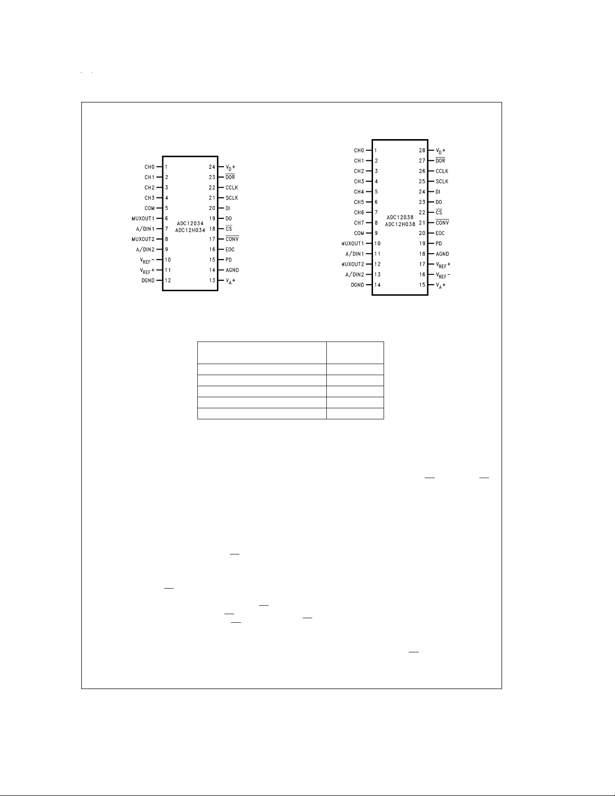
Connection Diagrams (Continued)
24-Pin Wide Body
SO Packages
28-Pin Wide Body
SO Packages
DS011354-8
Top View
Ordering Information
Industrial Temperature Range Package
−40˚C ≤ T
ADC12H030CIWM, ADC12030CIWM M16B
ADC12H032CIWM, ADC12032CIWM M20B
ADC12H034CIN, ADC12034CIN N24C
ADC12H034CIWM, ADC12034CIWM M24B
ADC12H038CIWM, ADC12038CIWM M28B
≤ +85˚C
A
Pin Descriptions
CCLK The clock applied to this input controls the
SCLK This is the serial data clock input. The clock
DI This is the serial data input pin. The data ap-
sucessive approximation conversion time
interval and the acquisition time. The rise
and fall times of the clock edges should not
exceed 1 µs.
applied to this input controls the rate at
which the serial data exchange occurs. The
rising edge loads the information on the DI
pin into the multiplexer address and mode
select shift register. This address controls
which channel of the analog input multiplexer (MUX) is selected and the mode of
operation for the A/D. With CS low the falling edge of SCLK shifts the data resulting
from the previous ADC conversion out on
DO, with the exception of the first bit of data.
When CS is low continously, the first bit of
the data is clocked out on the rising edge of
EOC (end of conversion). When CS is
toggled the falling edge of CS always clocks
out the first bit of data. CS should be
brought low when SCLK is low. The rise and
fall times of the clock edges should not exceed 1 µs.
plied to this pin is shifted by the rising edge
of SCLK into the multiplexer address and
DS011354-9
Top View
mode select register.
5
show the assignment of the multiplexer
address and the mode select data.
DO The data output pin. This pin is an active
EOC This pin is an active push/pull output and in-
CS
push/pull output when CS is low. When CS
is high, this output is TRI-STATE. The A/D
conversion result (D0–D12) and converter
status data are clocked out by the falling
edge of SCLK on this pin. The word length
and format of this result can vary (see
1
). The word length and format are controlled by the data shifted into the multiplexer address and mode select register
(see
Table 5
dicates the status of the ADC12030/2/4/8.
When low, it signals that the A/D is busy with
a conversion, auto-calibration, auto-zero or
power down cycle. The rising edge of EOC
signals the end of one of these cycles.
This is the chip select pin. When a logic low
is applied to this pin, the rising edge of
SCLK shifts the data on DI into the address
register. This low also brings DO out of
TRI-STATE. With CS low the falling edge of
SCLK shifts the data resulting from the previous ADC conversion out on DO, with the
Table 2
through
Table
Table
).
www.national.com3

Pin Descriptions (Continued)
exception of the first bit of data. When CS is
low continously, the first bit of the data is
clocked out on the rising edge of EOC (end
of conversion). When CS is toggled the falling edge of CS always clocks out the first bit
of data. CS should be brought low when
SCLK is low. The falling edge of CS resets a
conversion in progress and starts the sequence for a new conversion. When CS is
brought back low during a conversion, that
conversion is prematurely terminated. The
data in the output latches may be corrupted.
Therefore, when CS is brought back low
during a conversion in progress the data
output at that time should be ignored. CS
may also be left continuously low. In this
case it is imperative that the correct number
of SCLK pulses be applied to the ADC in order to remain synchronous. After the ADC
supply power is applied it expects to see 13
clock pulses for each I/O sequence. The
number of clock pulses the ADC expects is
the same as the digital output word length.
This word length can be modified by the
data shifted in on the DO pin.
the data required.
DOR
This is the data output ready pin.This pin is
an active push/pull output. It is low when the
conversion result is being shifted out and
goes high to signal that all the data has
been shifted out.
CONV
Alogic low is required on this pin to program
any mode or change the ADC’s configuration as listed in the Mode Programming
Table5
such as 12-bit conversion, 8-bit conversion, Auto Cal, Auto Zero etc. When this
pin is high the ADC is placed in the read
data only mode. While in the read data only
mode, bringing CS low and pulsing SCLK
will only clock out on DO any data stored in
the ADCs output shift register. The data on
DI will be neglected. A new conversion will
not be started and the ADC will remain in
the mode and/or configuration previously
programmed. Read data only cannot be
performed while a conversion, Auto-Cal or
Auto-Zero are in progress.
PD This is the power down pin. When PD is
high the A/D is powered down; when PD is
low the A/D is powered up. The A/D takes a
maximum of 250 µs to power up after the
command is given.
CH0–CH7 These are the analog inputs of the MUX. A
channel input is selected by the address information at the DI pin, which is loaded on
the rising edge of SCLK into the address
register (See
Tables 2, 3, 4
The voltage applied to these inputs should
not exceed V
ing this range on an unselectedchannel will
+ or go below GND. Exceed-
A
corrupt the reading of a selected channel.
COM This pin is another analog input pin. It is
used as a pseudo ground when the analog
multiplexer is single-ended.
Table5
).
details
MUXOUT1,
MUXOUT2
These are the multiplexer output
pins.
A/DIN1, /DIN2 These are the converter input pins. MUX-
OUT1 is usually tied to A/DIN1. MUXOUT2
is usually tied toA/DIN2. If external circuitry
is placed between MUXOUT1 and A/DIN1,
or MUXOUT2 and A/DIN2 it may be necessary to protect these pins. The voltage at
these pins should not exceed V
low AGND (see
+ This is the positive analog voltage reference
V
REF
input. In order to maintain accuracy, the
voltage range of V
V
−) is 1 VDCto 5.0 VDCand the voltage
REF
at V
REF
for recommended bypassing.
− The negative voltage reference input. In or-
V
REF
der to maintain accuracy, the voltage at this
Figure 5
REF(VREF
+ cannot exceed VA+. See
pin must not go below GND or exceed V
(See
Figure 6
).
+, VD+ These are the analog and digital power sup-
V
A
ply pins. V
gether on the chip. These pins should be
A
+
+
and V
are not connected to-
D
+
or go be-
A
).
=
+−
V
REF
Figure 6
A
tied to the same power supply and bypassed separately (see
ating voltage range of V
4.5 V
to 5.5 VDC.
DC
DGND This is the digital ground pin (see
AGND This is the analog ground pin (see
Figure 6
). The oper-
+ and VD+is
A
Figure 6
Figure 6
+.
).
).
www.national.com 4
Absolute Maximum Ratings (Notes 1, 2)
If Military/Aerospace specified devices are required,
please contact the National Semiconductor Sales Office/
Distributors for availability and specifications.
Positive Supply Voltage
+
=
+=VD+) 6.5V
V
(V
Voltage at Inputs and Outputs
Voltage at Analog Inputs
|V
Input Current at Any Pin (Note 3)
Package Input Current (Note 3)
Package Dissipation at
ESD Susceptability (Note 5)
A
+
except CH0–CH7 and COM −0.3V to V
CH0–CH7 and COM GND −5V to V
+−VD+| 300 mV
A
=
25˚C (Note 4) 500 mW
T
A
+0.3V
+
±
30 mA
±
120 mA
+5V
Human Body Model 1500V
Operating Ratings (Notes 1, 2)
Operating Temperature Range T
ADC12030CIWM,
ADC12H030CIWM,
ADC12032CIWM,
ADC12H032CIWM,
ADC12034CIN, ADC12034CIWM,
ADC12H034CIN,
ADC12H034CIWM,
ADC12038CIWM,
ADC12H038CIWM −40˚C ≤ T
Supply Voltage (V
+−VD+| ≤ 100 mV
|V
A
+ 0VtoVA+
V
REF
− 0VtoV
V
REF
V
REF(VREF
Common Mode Voltage Range
V
REF
+
=
+=VD+) +4.5V to +5.5V
V
A
+−V
−) 1V to VA+
REF
MIN
≤ TA≤ T
A
≤ +85˚C
Soldering Information
N Packages (10 seconds) 260˚C
SO Package (Note 6):
Vapor Phase (60 seconds) 215˚C
Infrared (15 seconds) 220˚C
Storage Temperature −65˚C to +150˚C
A/DIN1, A/DIN2, MUXOUT1
and MUXOUT2 Voltage Range 0V to V
A/D IN Common Mode
Voltage Range
0.1 VA+ to 0.6 VA+
0V to VA+
Converter Electrical Characteristics
The following specifications apply for V
sion mode, f
ADC12030, ADC12032, ADC12034 and ADC12038, R
input with fixed 2.048V common-mode voltage, and 10(tCK) acquisition time unless otherwise specified. Boldface limits apply
for T
A
Symbol Parameter Conditions Typical
=
=
f
CK
=
=
T
J
8 MHz for the ADC12H030, ADC12H032, ADC12H034 and ADC12H038, f
SK
to T
T
MIN
; all other limits T
MAX
+
=
+=VD+=+5.0 VDC,V
V
A
=
=
T
A
J
+=+4.096 VDC,V
REF
=
25Ω, source impedance for V
S
25˚C. (Notes 7, 8, 9)
−=0VDC, 12-bit + sign conver-
REF
+ and V
REF
(Note 10)
=
=
f
CK
REF
5 MHz for the
SK
− ≤ 25Ω, fully-differential
Limits
(Note 11)
Units
(Limits)
STATIC CONVERTER CHARACTERISTICS
Resolution with No
12 + sign Bits (min)
Missing Codes
+ILE Positive Integral Linearity Error After Auto-Cal (Notes 12, 18)
−ILE Negative Integral Linearity Error After Auto-Cal (Notes 12, 18)
DNL Differential Non-Linearity After Auto-Cal
Positive Full-Scale Error After Auto-Cal (Notes 12, 18)
Negative Full-Scale Error After Auto-Cal (Notes 12, 18)
Offset Error After Auto-Cal (Notes 5, 18)
V
(+)=VIN(−)=2.048V
IN
DC Common Mode Error After Auto-Cal (Note 15)
TUE Total Unadjusted Error After Auto-Cal
±
1/2
±
1/2
±
1/2
±
1/2
±
1/2
±
2
±
1 LSB
±
1 LSB (max)
±
1 LSB (max)
±
1 LSB (max)
±
3.0 LSB (max)
±
3.0 LSB (max)
±
2 LSB (max)
±
3.5 LSB (max)
(Notes 12, 13, 14)
Resolution with No
8-bit + sign mode 8 + sign Bits (min)
Missing Codes
+INL Positive Integral Linearity Error 8-bit + sign mode (Note 12)
−INL Negative Integral Linearity Error 8-bit + sign mode (Note 12)
DNL Differential Non-Linearity 8-bit + sign mode
Positive Full-Scale Error 8-bit + sign mode (Note 12)
Negative Full-Scale Error 8-bit + sign mode (Note 12)
±
1/2 LSB (max)
±
1/2 LSB (max)
±
3/4 LSB (max)
±
1/2 LSB (max)
±
1/2 LSB (max)
REF
MAX
+
+
A
www.national.com5
Converter Electrical Characteristics (Continued)
+
Offset Error
=
+=VD+=+5.0 VDC,V
V
A
=
25Ω, source impedance for V
S
=
=
T
25˚C. (Notes 7, 8, 9)
A
J
after Auto-Zero (Note 13)
V
(+)=VIN(−)=+ 2.048V
IN
after Auto-Zero
(Notes 12, 13, 14)
+
=
±
10
+5V
=
V
+4.096V
REF
=
1 kHz, V
IN
=
20 kHz, V
IN
=
f
40 kHz, V
IN
=
, where S/(N+D) drops 3 dB 31 kHz
5V
IN
PP
=
1 kHz, V
IN
=
20 kHz, V
IN
=
f
40 kHz, V
IN
=
±
5V, where S/(N+D) drops 3 dB 40 kHz
IN
=
+5.0V or
IN
=
0V
IN
+=+4.096 VDC,V
REF
−=0VDC, 12-bit + sign conver-
REF
+ and V
REF
(Note 10)
=
=
f
CK
REF
±
0.05 LSB
5 MHz for the
SK
− ≤ 25Ω, fully-differential
Limits
(Note 11)
±
1/2 LSB (max)
±
3/4 LSB (max)
(Limits)
%
±
0.5
±
0.5
±
0.5
±
0.5 LSB
±
0.5 LSB
PP,VREF
PP,VREF
PP,VREF
REF
5V, V
5V, V
+
=
5.0V 69.4 dB
+
=
5.0V 68.3 dB
+=5.0V 65.7 dB
+
=
5.0V 77.0 dB
+
=
5.0V 73.9 dB
REF
+
=
5.0V 67.0 dB
REF
±
0.1
=
5V
IN
=
5V
IN
=
5V
IN
=
±
5V, V
IN
=
±
IN
=
±
IN
±
1 LSB (max)
±
1.5 LSB (max)
±
1.5 LSB (max)
±
1.0 µA (max)
+ + 0.05 V (max)
A
10 pF
The following specifications apply for V
sion mode, f
ADC12030, ADC12032, ADC12034 and ADC12038, R
input with fixed 2.048V common-mode voltage, and 10(tCK) acquisition time unless otherwise specified. Boldface limits apply
for T
A
=
=
f
CK
=
=
T
J
8 MHz for the ADC12H030, ADC12H032, ADC12H034 and ADC12H038, f
SK
to T
T
MIN
; all other limits T
MAX
Symbol Parameter Conditions Typical
STATIC CONVERTER CHARACTERISTICS
Offset Error 8-bit + sign mode,
TUE Total Unadjusted Error 8-bit + sign mode
Multiplexer Channel
to Channel Matching
Power Supply Sensitivity V
+ Full-Scale Error
− Full-Scale Error
+ Integral Linearity Error
− Integral Linearity Error
Output Data from (Note 20) +10 LSB (max)
“12-Bit Conversion of Offset” −10 LSB (min)
(see
Table 5
)
Output Data from (Note 20) 4095 LSB (max)
“12-Bit Conversion of Full-Scale” 4093 LSB (min)
(see
Table 5
)
UNIPOLAR DYNAMIC CONVERTER CHARACTERISTICS
S/(N+D) Signal-to-Noise Plus f
Distortion Ratio f
−3 dB Full Power Bandwidth V
DIFFERENTIAL DYNAMIC CONVERTER CHARACTERISTICS
S/(N+D) Signal-to-Noise Plus f
Distortion Ratio f
−3 dB Full Power Bandwidth V
REFERENCE INPUT, ANALOG INPUTS AND MULTIPLEXER CHARACTERISTICS
C
REF
C
A/D
Reference Input Capacitance 85 pF
A/DIN1 and A/DIN2 Analog 75 pF
Input Capacitance
A/DIN1 and A/DIN2 Analog V
Input Leakage Current V
CH0–CH7 and COM GND − 0.05 V (min)
Input Voltage V
C
CH
C
MUXOUT
CH0–CH7 and COM
Input Capacitance
MUX Output Capacitance 20 pF
Units
www.national.com 6
Converter Electrical Characteristics (Continued)
+
The following specifications apply for V
sion mode, f
ADC12030, ADC12032, ADC12034 and ADC12038, R
input with fixed 2.048V common-mode voltage, and 10(tCK) acquisition time unless otherwise specified. Boldface limits apply
for T
A
=
=
f
CK
=
=
T
J
8 MHz for the ADC12H030, ADC12H032, ADC12H034 and ADC12H038, f
SK
to T
T
MIN
; all other limits T
MAX
Symbol Parameter Conditions Typical
REFERENCE INPUT, ANALOG INPUTS AND MULTIPLEXER CHARACTERISTICS
Off Channel Leakage (Note 16) On Channel=5V and −0.01 −0.3 µA (min)
CH0–CH7 and COM Pins Off Channel=0V
On Channel Leakage (Note 16) On Channel=5V and 0.01 0.3 µA (max)
CH0–CH7 and COM Pins Off Channel=0V
MUXOUT1 and MUXOUT2 V
Leakage Current V
R
MUX On Resistance V
ON
R
Matching Channel V
ON
to Channel V
Channel to Channel Crosstalk V
MUX Bandwidth 90 kHz
=
+=VD+=+5.0 VDC,V
V
A
=
25Ω, source impedance for V
S
=
=
T
25˚C. (Notes 7, 8, 9)
A
J
+=+4.096 VDC,V
REF
−=0VDC, 12-bit + sign conver-
REF
+ and V
REF
(Note 10)
=
=
f
CK
REF
5 MHz for the
SK
− ≤ 25Ω, fully-differential
Limits
(Note 11)
On Channel=0V and 0.01 0.3 µA (max)
Off Channel=5V
On Channel=0V and −0.01 −0.3 µA (min)
Off Channel=5V
=
MUXOUT
MUXOUT
IN
V
MUXOUT
IN
MUXOUT
IN
5.0V or 0.01 0.3 µA (max)
=
0V
=
2.5V and 850 1150 Ω (max)
=
2.4V
=
2.5V and 5
=
2.4V
=
5V
=
40 kHz −72 dB
PP,fIN
Units
(Limits)
%
DC and Logic Electrical Characteristics
The following specifications apply for V
sion mode, f
ADC12030, ADC12032, ADC12034 and ADC12038, R
input with fixed 2.048V common-mode voltage, and 10(t
for T
A
=
=
f
CK
=
=
T
J
8 MHz for the ADC12H030, ADC12H032, ADC12H034 and ADC12H038, f
SK
to T
T
MIN
; all other limits T
MAX
+
=
+=VD+=+5.0 VDC,V
V
A
=
=
T
A
J
+=+4.096 VDC,V
REF
=
25Ω, source impedance for V
S
) acquisition time unless otherwise specified. Boldface limits apply
CK
25˚C. (Notes 7, 8, 9)
−=0VDC, 12-bit + sign conver-
REF
REF
+ and V
=
=
f
CK
REF
5 MHz for the
SK
− ≤ 25Ω, fully-differential
Symbol Parameter Conditions Typical Limits Units
(Note 10) (Note 11) (Limits)
CCLK, CS, CONV, DI, PD AND SCLK INPUT CHARACTERISTICS
+
V
V
I
I
Logical “1” Input Voltage V
IN(1)
Logical “0” Input Voltage V
IN(0)
Logical “1” Input Current V
IN(1)
Logical “0” Input Current V
IN(0)
=
5.5V 2.0 V (min)
+
=
4.5V 0.8 V (max)
=
5.0V 0.005 1.0 µA (max)
IN
=
0V −0.005 −1.0 µA (min)
IN
DO, EOC AND DOR DIGITAL OUTPUT CHARACTERISTICS
V
V
I
OUT
+I
−I
Logical “1” Output Voltage V
OUT(1)
Logical “0” Output Voltage V
OUT(0)
TRI-STATE®Output Current V
Output Short Circuit Source Current V
SC
Output Short Circuit Sink Current V
SC
=
4.5V, I
+
=
V
4.5V, I
+
=
4.5V, I
=
OUT
=
V
OUT
=
OUT
=
OUT
=
−360 µA 2.4 V (min)
OUT
=
−10µA 4.25 V (min)
OUT
=
1.6 mA 0.4 V (max)
OUT
0V −0.1 −3.0 µA (max)
5V 0.1 3.0 µA (max)
0V 14 6.5 mA (min)
+168.0 mA (min)
V
D
+
POWER SUPPLY CHARACTERISTICS
I
+ Digital Supply Current Awake 1.6 2.5 mA (max)
D
ADC12030, ADC12032, ADC12034 CS=HIGH, Powered Down, CCLK on
and ADC12038 CS=HIGH, Powered Down, CCLK off
600 µA
20 µA
Digital Supply Current Awake 2.3 3.2 mA
ADC12H030, ADC12H032, CS=HIGH, Powered Down, CCLK on
ADC12H034 and ADC12H038 CS=HIGH, Powered Down, CCLK off
0.9 mA
20 µA
www.national.com7
DC and Logic Electrical Characteristics (Continued)
+
The following specifications apply for V
sion mode, f
ADC12030, ADC12032, ADC12034 and ADC12038, R
input with fixed 2.048V common-mode voltage, and 10(tCK) acquisition time unless otherwise specified. Boldface limits apply
for T
A
=
=
f
CK
=
=
T
J
8 MHz for the ADC12H030, ADC12H032, ADC12H034 and ADC12H038, f
SK
to T
T
MIN
; all other limits T
MAX
Symbol Parameter Conditions Typical Limits Units
POWER SUPPLY CHARACTERISTICS
+ Positive Analog Supply Current Awake 2.7 4.0 mA (max)
I
A
I
Reference Input Current Awake 70 µA
REF
=
+=VD+=+5.0 VDC,V
V
A
=
25Ω, source impedance for V
S
=
=
T
25˚C. (Notes 7, 8, 9)
A
J
CS=HIGH, Powered Down, CCLK on
CS=HIGH, Powered Down, CCLK off
CS=HIGH, Powered Down
+=+4.096 VDC,V
REF
−=0VDC, 12-bit + sign conver-
REF
REF
+ and V
=
=
f
CK
REF
5 MHz for the
SK
− ≤ 25Ω, fully-differential
(Note 10) (Note 11) (Limits)
10 µA
0.1 µA
0.1 µA
AC Electrical Characteristics
The following specifications apply for V
sion mode, t
MHz for the ADC12030, ADC12032, ADC12034 and ADC12038, R
fully-differential input with fixed 2.048V common-mode voltage, and 10(tCK) acquisition time unless otherwise specified. Bold-
face limits apply for T
Symbol Parameter Conditions Typical
=
=
t
3 ns, f
r
f
CK
=
T
A
J
+
=
+=VD+=+5.0 VDC,V
V
=
f
SK
=
T
MIN
A
=
8 MHz for the ADC12H030, ADC12H032, ADC12H034 and ADC12H038, f
to T
; all other limits T
MAX
(Note 10)
+=+4.096 VDC,V
REF
=
25Ω, source impedance for V
S
=
=
T
25˚C. (Note 17)
A
J
ADC12H030/2/4/8 ADC12030/2/4/8 Units
Limits Limits
REF
−=0VDC, 12-bit + sign conver+ and V
REF
CK
REF
=
f
SK
− ≤ 25Ω,
(Limits)
(Note 11) (Note 11)
f
CK
Conversion Clock 10 85MHz (max)
(CCLK) Frequency 1 MHz (min)
f
SK
Serial Data Clock 10 85MHz (max)
SCLK Frequency 0 Hz (min)
Conversion Clock 40 40
Duty Cycle 60 60
Serial Data Clock 40 40
Duty Cycle 60 60
t
C
Conversion Time 12-Bit + Sign or 12-Bit 44(tCK) 44(tCK) 44(tCK) (max)
%
%
%
%
5.5 8.8 µs (max)
8-Bit + Sign or 8-Bit 21(t
) 21(tCK) 21(tCK) (max)
CK
2.625 4.2 µs (max)
t
A
Acquisition Time 6 Cycles Programmed 6(tCK) 6(tCK) 6(tCK) (min)
(Note 19) 7(t
) 7(tCK) (max)
CK
0.75 1.2 µs (min)
0.875 1.4 µs (max)
10 Cycles Programmed 10(t
) 10(tCK) 10(tCK) (min)
CK
11(t
) 11(tCK) (max)
CK
1.25 2.0 µs (min)
1.375 2.2 µs (max)
18 Cycles Programmed 18(t
) 18(tCK) 18(tCK) (min)
CK
19(t
) 19(tCK) (max)
CK
2.25 3.6 µs (min)
2.375 3.8 µs (max)
34 Cycles Programmed 34(t
) 34(tCK) 34(tCK) (min)
CK
35(t
) 35(tCK) (max)
CK
4.25 6.8 µs (min)
4.375 7.0 µs (max)
=
(min)
(max)
(min)
(max)
5
www.national.com 8
AC Electrical Characteristics (Continued)
+
The following specifications apply for V
sion mode, t
MHz for the ADC12030, ADC12032, ADC12034 and ADC12038, R
fully-differential input with fixed 2.048V common-mode voltage, and 10(tCK) acquisition time unless otherwise specified. Bold-
face limits apply for T
=
=
t
3 ns, f
r
f
=
CK
=
=
T
A
J
Symbol Parameter Conditions Typical
t
CKAL
t
AZ
t
SYNC
Self-Calibration Time 4944(tCK) 4944(tCK) 4944(tCK) (max)
Auto-Zero Time 76(tCK) 76(tCK) 76(tCK) (max)
Self-Calibration 2(tCK) 2(tCK) 2(tCK) (min)
or Auto-Zero 3(t
Synchronization Time 0.250 0.40 µs (min)
from DOR 0.375 0.60 µs (max)
t
DOR
DOR High Time 9(tSK) 9(tSK) 9(tSK) (max)
when CS is Low
Continuously for Read
Data and Software
Power Up/Down
t
CONV
CONV Valid Data Time 8(tSK) 8(tSK) 8(tSK) (max)
=
+=VD+=+5.0 VDC,V
V
A
=
f
8 MHz for the ADC12H030, ADC12H032, ADC12H034 and ADC12H038, f
SK
to T
T
MIN
; all other limits T
MAX
(Note 10)
+=+4.096 VDC,V
REF
=
25Ω, source impedance for V
S
=
=
T
A
25˚C. (Note 17)
J
ADC12H030/2/4/8 ADC12030/2/4/8 Units
Limits Limits
−=0VDC, 12-bit + sign conver-
REF
(Note 11) (Note 11)
618.0 988.8 µs (max)
9.5 15.2 µs (max)
) 3(tCK) (max)
CK
1.125 1.8 µs (max)
1.0 1.6 µs (max)
REF
+ and V
CK
REF
=
f
SK
− ≤ 25Ω,
(Limits)
=
5
AC Electrical Characteristics
The following specifications apply for V
sion mode, t
MHz for the ADC12030, ADC12032, ADC12034 and ADC12038, R
fully-differential input with fixed 2.048V common-mode voltage, and 10(tCK) acquisition time unless otherwise specified. Bold-
face limits apply for T
Symbol Parameter Conditions Typical
t
HPU
=
=
t
3 ns, f
r
f
CK
=
T
A
J
Hardware Power-Up Time, Time from 140 250 µs (max)
+
=
+=VD+=+5.0 VDC,V
V
=
f
SK
=
T
MIN
A
=
8 MHz for the ADC12H030, ADC12H032, ADC12H034 and ADC12H038, f
to T
; all other limits T
MAX
+=+4.096 VDC,V
REF
=
25Ω, source impedance for V
S
=
=
T
25˚C. (Note 17)
A
J
REF
(Note 10)
−=0VDC, 12-bit + sign conver+ and V
REF
Limits
(Note 11)
CK
REF
=
f
SK
− ≤ 25Ω,
(Limits)
PD Falling Edge to EOC Rising Edge
t
SPU
Software Power-Up Time, Time from
Serial Data Clock Falling Edge to 140 250 µs (max)
EOC Rising Edge
t
ACC
Access Time Delay from 20 50 ns (max)
CS Falling Edge to DO Data Valid
t
SET-UP
Set-Up Time of CS Falling Edge to 30 ns (min)
Serial Data Clock Rising Edge
t
DELAY
Delay from SCLK Falling 0 5 ns (min)
Edge to CS Falling Edge
=
t1H,t0HDelay from CS Rising Edge to R
L
=
3k, C
100 pF 40 100 ns (max)
L
DO TRI-STATE
t
HDI
DI Hold Time from Serial Data 5 15 ns (min)
Clock Rising Edge
t
SDI
DI Set-Up Time from Serial Data 5 10 ns (min)
Clock Rising Edge
=
t
HDO
DO Hold Time from Serial Data R
L
=
3k, C
100 pF 25 50 ns (max)
L
Clock Falling Edge 5 ns (min)
t
DDO
Delay from Serial Data Clock 35 50 ns (max)
Falling Edge to DO Data Valid
=
5
Units
www.national.com9
AC Electrical Characteristics (Continued)
+
The following specifications apply for V
sion mode, t
MHz for the ADC12030, ADC12032, ADC12034 and ADC12038, R
fully-differential input with fixed 2.048V common-mode voltage, and 10(tCK) acquisition time unless otherwise specified. Bold-
face limits apply for T
=
=
t
3 ns, f
r
f
=
CK
=
=
T
A
J
Symbol Parameter Conditions Typical
t
RDO
DO Rise Time, TRI-STATE to High R
DO Rise Time, Low to High 10 30 ns (max)
t
FDO
DO Fall Time, TRI-STATE to Low R
DO Fall Time, High to Low 12 30 ns (max)
t
CD
Delay from CS Falling Edge 25 45 ns (max)
to DOR Falling Edge
t
SD
Delay from Serial Data Clock Falling 25 45 ns (max)
Edge to DOR Rising Edge
C
IN
C
OUT
Capacitance of Logic Inputs 10 pF
Capacitance of Logic Outputs 20 pF
Note 1: Absolute Maximum Ratings indicate limits beyond which damage to the device may occur. Operating Ratings indicate conditions for which the device is functional, but do not guarantee specific performance limits. For guaranteed specifications and test conditions, see the Electrical Characteristics. The guaranteed specifications apply only for the test conditions listed. Some performance characteristics may degrade when the device is not operated under the listed test conditions.
Note 2: All voltages are measured with respect to GND, unless otherwise specified.
Note 3: When the input voltage (V
The 120 mA maximum package input current rating limits the number of pins that can safely exceed the power supplies with an input current of 30 mA to four.
Note 4: The maximum power dissipation must be derated at elevated temperatures and is dictated by T
allowable power dissipation at any temperature is P
max=150˚C. The typical thermal resistance (θJA) of these parts when board mounted follow:
T
J
Note 5: The human body model is a 100 pF capacitor discharged through a 1.5 kΩ resistor into each pin.
Note 6: See AN450 “Surface Mounting Methods and Their Effect on Product Reliability” or the section titled “Surface Mount” found in any post 1986 National Semi-
conductor Linear Data Book for other methods of soldering surface mount devices.
Note 7: Two on-chip diodes are tied to each analog input through a series resistor as shown below. Input voltage magnitude up to 5V above V
will not damage this device. However, errors in the A/D conversion can occur (if these diodes are forward biased by more than 50 mV) if the input voltage magnitude
of selected or unselected analog input go above V
to ensure accurate conversions.
V
DC
) at any pin exceeds the power supplies (V
IN
=
+=VD+=+5.0 VDC,V
V
A
=
f
8 MHz for the ADC12H030, ADC12H032, ADC12H034 and ADC12H038, f
SK
to T
T
MIN
; all other limits T
MAX
=
3k, C
L
=
3k, C
L
IN
=
max − TA)/θJAor the number given in the Absolute Maximum Ratings, whichever is lower. For this device,
(T
D
J
+=+4.096 VDC,V
REF
=
25Ω, source impedance for V
S
=
=
T
25˚C. (Note 17)
A
J
(Note 10)
=
100 pF 10 30 ns (max)
L
=
100 pF 12 30 ns (max)
L
<
GND or V
>
VA+orVD+), the current at that pin should be limited to 30 mA.
IN
max, θJAand the ambient temperature, TA. The maximum
J
−=0VDC, 12-bit + sign conver-
REF
+ and V
REF
Limits
(Note 11)
Thermal
Part Number Resistance
θ
JA
ADC12H030CIWM, ADC12030CIWM 70˚C/W
ADC12H032CIWM, ADC12032CIWM 64˚C/W
ADC12H034CIN, ADC12034CIN 42˚C/W
ADC12H034CIWM, ADC12034CIWM 57˚C/W
ADC12H038CIWM, ADC12038CIWM 50˚C/W
+ or below GND by more than 50 mV. As an example, if VA+ is 4.5 VDC, full-scale input voltage must be ≤4.55
A
=
f
CK
SK
− ≤ 25Ω,
REF
Units
(Limits)
+ or 5V below GND
A
=
5
Note 8: To guarantee accuracy, it is required that the V
pin.
www.national.com 10
+ and VD+ be connected together to the same power supply with separate bypass capacitors at each V
A
DS011354-2
+
AC Electrical Characteristics (Continued)
Note 9: With the test condition for V
=
Note 10: Typicals are at T
Note 11: Tested limits are guaranteed to National’s AOQL (Average Outgoing Quality Level).
Note 12: Positive integral linearity error is defined as the deviation of the analog value, expressed in LSBs, from the straight line that passes through positive
full-scale and zero. For negative integral linearity error, the straight line passes through negative full-scale and zero (see
Note 13: Zero error is a measure of the deviation from the mid-scale voltage (a code of zero), expressed in LSB. It is the worst-case value of the code transitions
between 1 to 0 and 0 to +1 (see
=
T
J
A
Figure 4
Note 14: Total unadjusted error includes offset, full-scale, linearity and multiplexer errors.
Note 15: The DC common-mode error is measured in the differential multiplexer mode with the assigned positive and negative input channels shorted together.
Note 16: Channel leakage current is measured after the channel selection.
Note 17: Timing specifications are tested at the TTL logic levels, V
to 1.4V.
Note 18: The ADC12030 family’s self-calibration technique ensures linearity and offset errors as specified, but noise inherent in the self-calibration process will re-
sult in a maximum repeatability uncertainty of 0.2 LSB.
Note 19: If SCLK and CCLK are driven from the same clock source, then t
Note 20: The “12-Bit Conversion of Offset” and “12-Bit Conversion of Full-Scale” modes are intended to test the functionality of the device. Therefore, the output
data from these modes are not an indication of the accuracy of a conversion result.
+−V
REF(VREF
25˚C and represent most likely parametric norm.
−) given as +4.096V, the 12-bit LSB is 1.0 mV and the 8-bit LSB is 16.0 mV.
REF
).
=
0.4V for a falling edge and V
IL
is 6, 10, 18 or 34 clock periods minimum and maximum.
A
Figures 2, 3
).
=
2.4V for a rising edge. TRI-STATEoutput voltage is forced
IH
DS011354-10
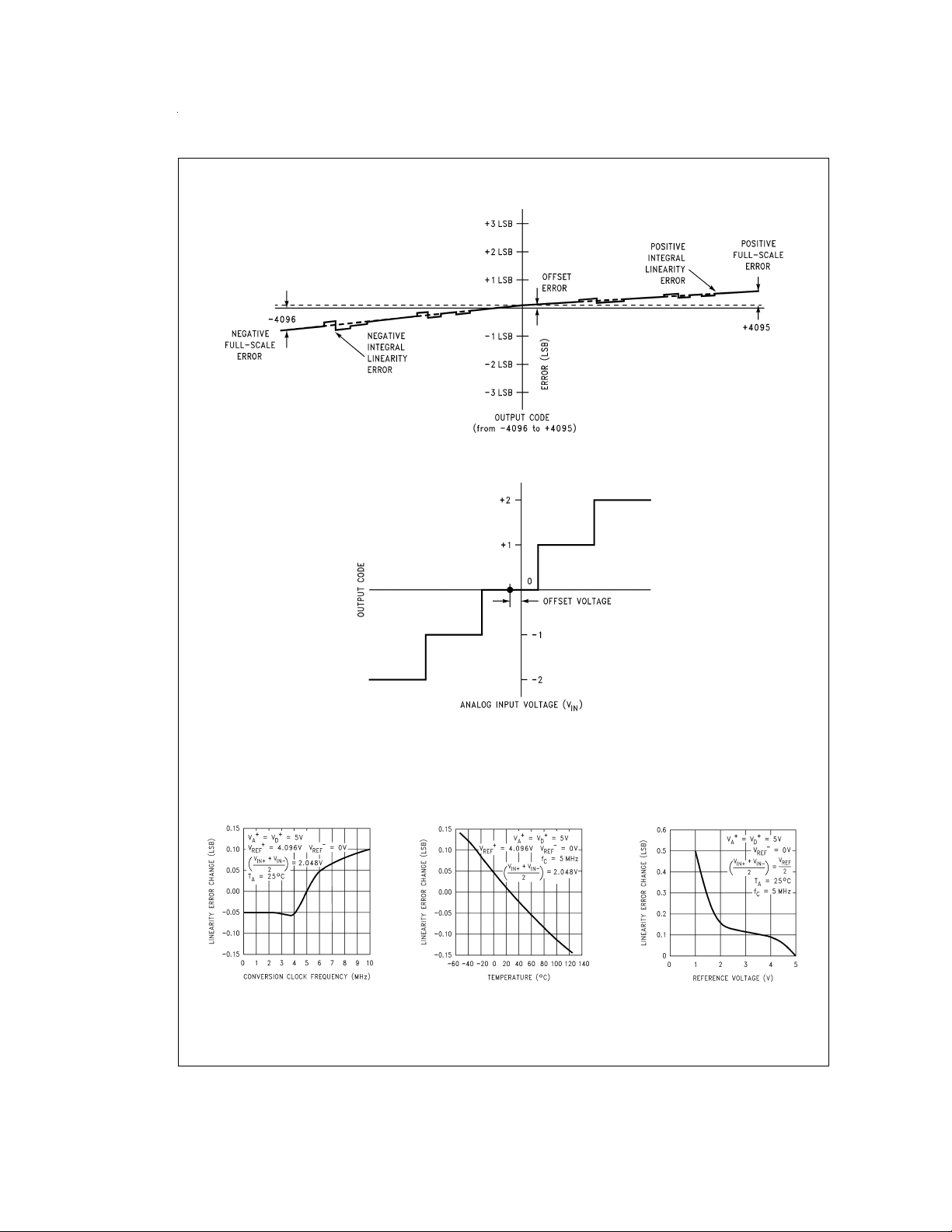
FIGURE 1. Transfer Characteristic
DS011354-11
FIGURE 2. Simplified Error Curve vs Output Code without Auto-Calibration or Auto-Zero Cycles
www.national.com11
AC Electrical Characteristics (Continued)
FIGURE 3. Simplified Error Curve vs Output Code after Auto-Calibration Cycle
DS011354-12
DS011354-13
FIGURE 4. Offset or Zero Error Voltage
Typical Performance Characteristics The following curves apply for 12-bit + sign mode after
auto-calibration unless otherwise specified. The performance for 8-bit + sign mode is equal to or better than shown. (Note 9)
Linearity Error Change
vs Clock Frequency
DS011354-53
www.national.com 12
Linearity Error Change
vs Temperature
Linearity Error Change
vs Reference Voltage
DS011354-54
DS011354-55
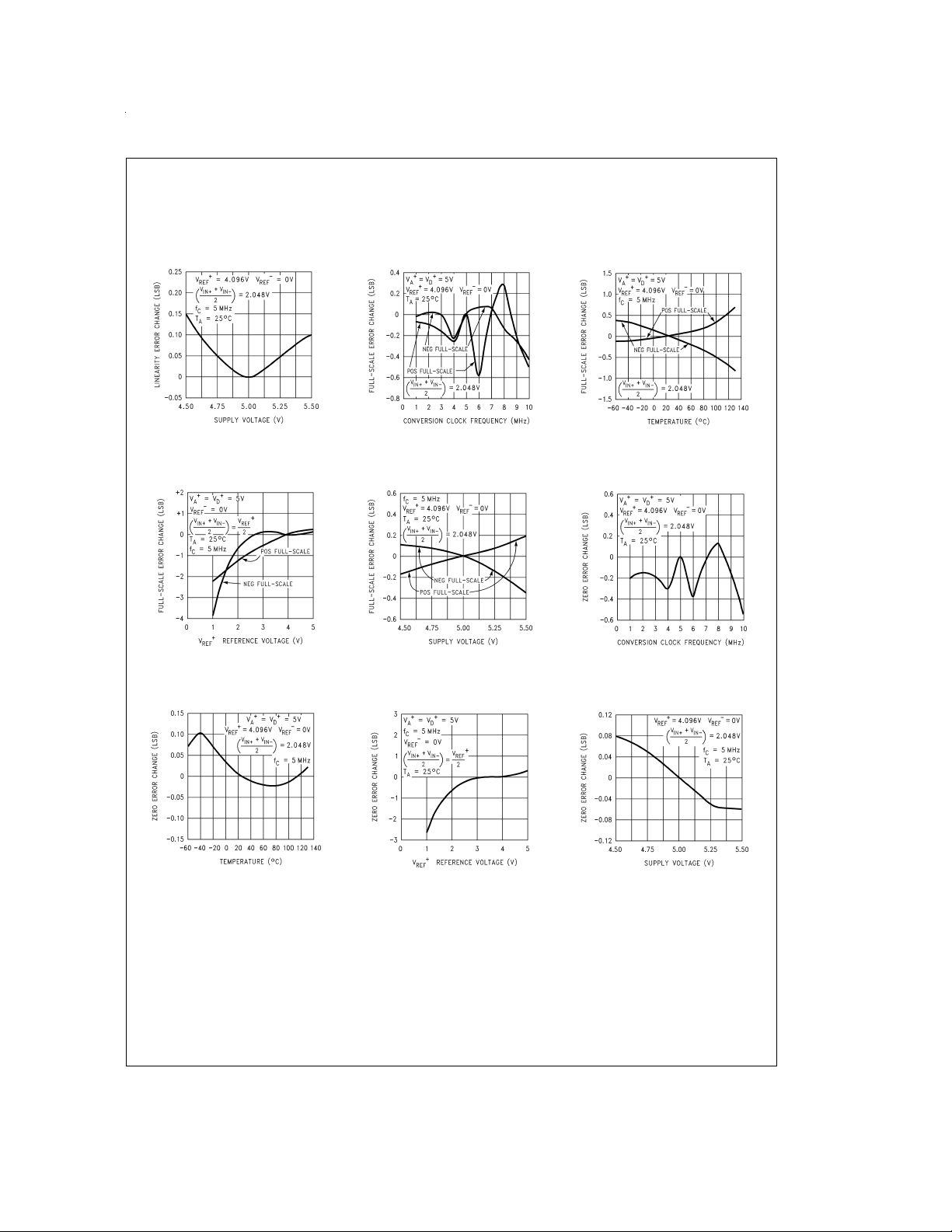
Typical PerformanceCharacteristics The following curves apply for 12-bit + sign mode after
auto-calibration unless otherwise specified. The performance for 8-bit + sign mode is equal to or better than shown. (Note
9) (Continued)
Linearity Error Change
vs Supply Voltage
Full-Scale Error Change
vs Reference Voltage
Zero Error Change
vs Temperature
DS011354-56
DS011354-59
Full-Scale Error Change
vs Clock Frequency
Full-Scale Error Change
vs Supply Voltage
Zero Error Change
vs Reference Voltage
DS011354-57
DS011354-60
Full-Scale Error Change
vs Temperature
DS011354-58
Zero Error Change
vs Clock Frequency
DS011354-61
Zero Error Change
vs Supply Voltage
DS011354-62
DS011354-63
DS011354-64
www.national.com13
 Loading...