


DS90C387
DS90C387/DS90CF388
Dual Pixel LVDS Display Interface (LDI)-SVGA/QXGA
General Description
The DS90C387/DS90CF388 transmitter/receiver pair is de-
signed to support dual pixel data transmission between Host
and Flat Panel Display up to QXGA resolutions. The trans-
mitter converts 48 bits (Dual Pixel 24-bit color) of CMOS/TTL
data into 8 LVDS (Low Voltage Differential Signalling) data
streams. Control signals (VSYNC, HSYNC, DE and two
user-defined signals) are sent during blanking intervals. At a
maximum dual pixel rate of 112MHz, LVDS data line speed is
672Mbps, providing a total throughput of 5.38Gbps (672
Megabytes per second). Two other modes are also sup-
ported. 24-bit color data (single pixel) can be clocked into the
transmitter at a maximum rate of 170MHz. In this mode, the
transmitter provides single-to-dual pixel conversion, and the
output LVDS clock rate is 85MHz maximum. The third mode
provides inter-operability with FPD-Link devices.
The LDI chipset is improved over prior generations of FPD-
Link devices and offers higher bandwidth support and longer
cable drive with three areas of enhancement. To increase
bandwidth, the maximum pixel clock rate is increased to 112
(170) MHz and 8 serialized LVDS outputs are provided.
Cable drive is enhanced with a user selectable pre-
emphasis feature that provides additional output current dur-
ing transitions to counteract cable loading effects. DC bal-
ancing on a cycle-to-cycle basis, is also provided to reduce
ISI (Inter-Symbol Interference). With pre-emphasis and DC
balancing, a low distortion eye-pattern is provided at the
receiver end of the cable. A cable deskew capability has
been added to deskew long cables of pair-to-pair skew of up
to +/−1 LVDS data bit time (up to 80 MHz Clock Rate). These
three enhancements allow cables 5+ meters in length to be
driven. This chipset is an ideal means to solve EMI and cable
size problems for high-resolution flat panel applications. It
provides a reliable interface based on LVDS technology that
delivers the bandwidth needed for high-resolution panels
while maximizing bit times, and keeping clock rates low to
reduce EMI and shielding requirements. For more details,
please refer to the “Applications Information” section of this
datasheet.
Features
n Complies with OpenLDI specification for digital display
interfaces
n 32.5 to 112/170MHz clock support for DS90C387, 40 to
112MHz clock support for DS90CF388
n Supports SVGA through QXGA panel resolutions
n Drives long, low cost cables
n Up to 5.38Gbps bandwidth
n Pre-emphasis reduces cable loading effects
n DC Balance data transmission provided by transmitter
reduces ISI distortion
n Cable Deskew of +/−1 LVDS data bit time (up to 80
MHz Clock Rate) of pair-to-pair skew at receiver inputs;
intra-pair skew tolerance of 300ps
n Dual pixel architecture supports interface to GUI and
timing controller; optional single pixel transmitter inputs
support single pixel GUI interface
n Transmitter rejects cycle-to-cycle jitter
n 5V tolerant on data and control input pins
n Programmable transmitter data and control strobe select
(rising or falling edge strobe)
n Backward compatible configuration select with FPD-Link
n Optional second LVDS clock for backward compatibility
w/ FPD-Link
n Support for two additional user-defined control signals in
DC Balanced mode
n Compatible with ANSI/TIA/EIA-644-1995 LVDS Standard
TRI-STATE
®
is a registered trademark of National Semiconductor Corporation.
May 2004
DS90C387/DS90CF388 Dual Pixel LVDS Display Interface (LDI)-SVGA/QXGA
© 2004 National Semiconductor Corporation DS100073 www.national.com
查询DS90C387供应商
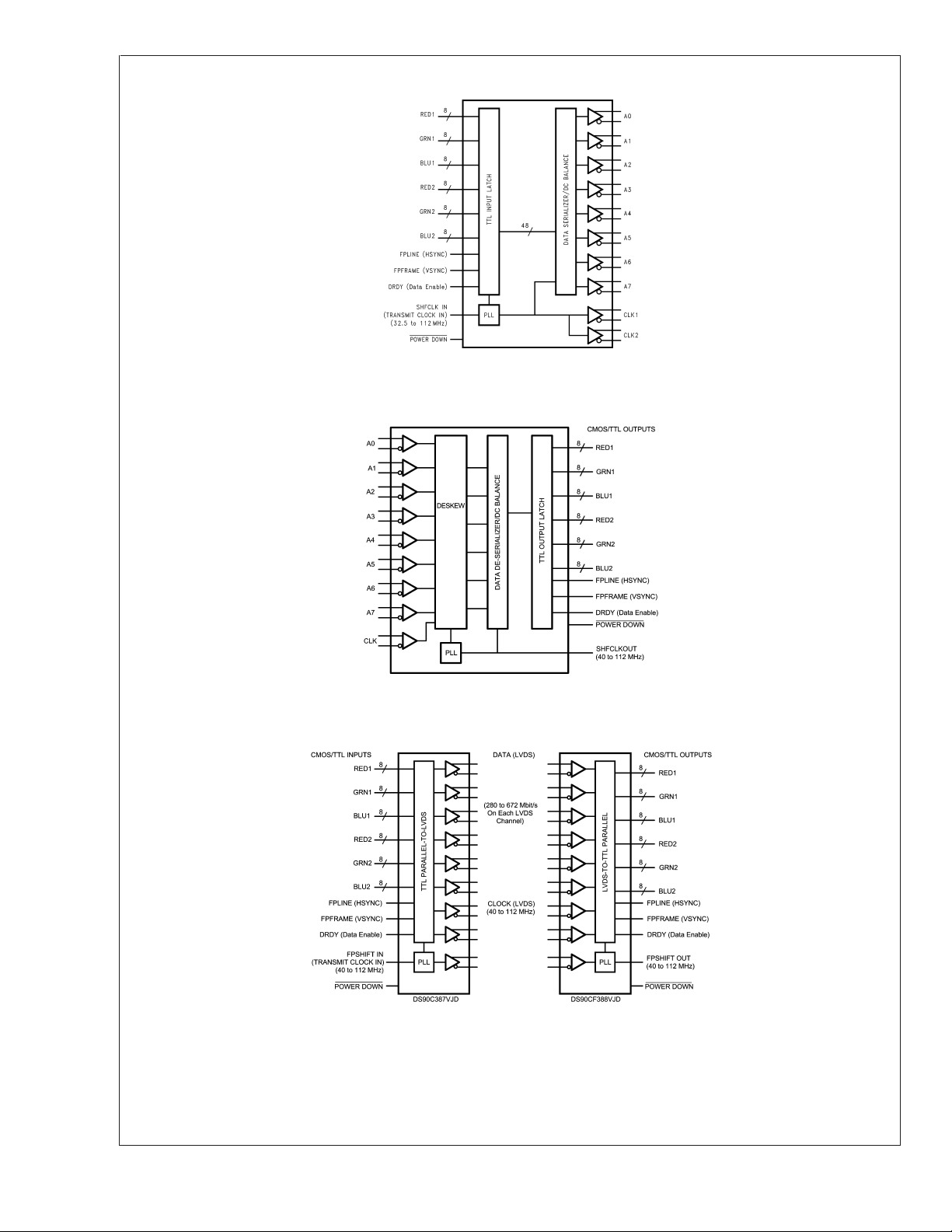
Transmitter Block Diagram
10007302
Receiver Block Diagram
10007303
Generalized Block Diagram
10007301
DS90C387/DS90CF388
www.national.com 2
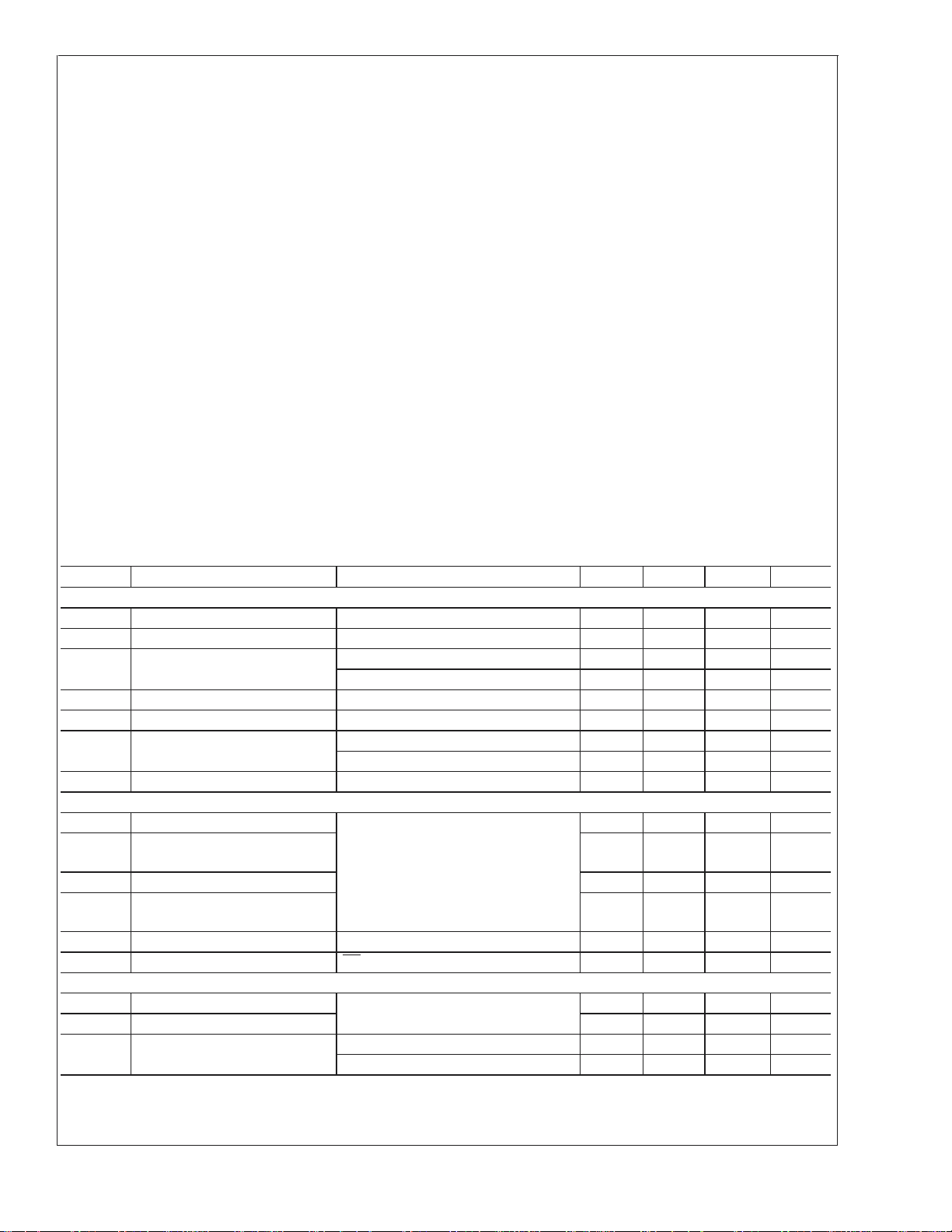
Absolute Maximum Ratings (Note 1)
If Military/Aerospace specified devices are required,
please contact the National Semiconductor Sales Office/
Distributors for availability and specifications.
Supply Voltage (V
CC
) −0.3V to +4V
CMOS/TTL Input Voltage −0.3V to +5.5V
CMOS/TTL Output
Voltage −0.3V to (V
CC
+ 0.3V)
LVDS Receiver Input
Voltage −0.3V to +3.6V
LVDS Driver Output
Voltage −0.3V to +3.6V
LVDS Output Short
Circuit Duration Continuous
Junction Temperature +150˚C
Storage Temperature −65˚C to +150˚C
Lead Temperature
(Soldering, 4 sec.) +260˚C
Maximum Package Power Dissipation Capacity
@
25˚C
100 TQFP Package:
DS90C387 2.8W
DS90CF388 2.8W
Package Derating:
DS90C387 18.2mW/˚C above +25˚C
DS90CF388 18.2mW/˚C above +25˚C
ESD Rating:
DS90C387
(HBM, 1.5kΩ, 100pF)
>
6kV
(EIAJ, 0Ω, 200pF)
>
300 V
DS90CF388
(HBM, 1.5kΩ, 100pF)
>
2kV
(EIAJ, 0Ω, 200pF)
>
200 V
Recommended Operating
Conditions
Min Nom Max Units
Supply Voltage (V
CC
) 3.0 3.3 3.6 V
Operating Free Air
Temperature (T
A)
−10 +25 +70 ˚C
Receiver Input Range 0 2.4 V
Supply Noise Voltage (V
CC
) 100 mV
p-p
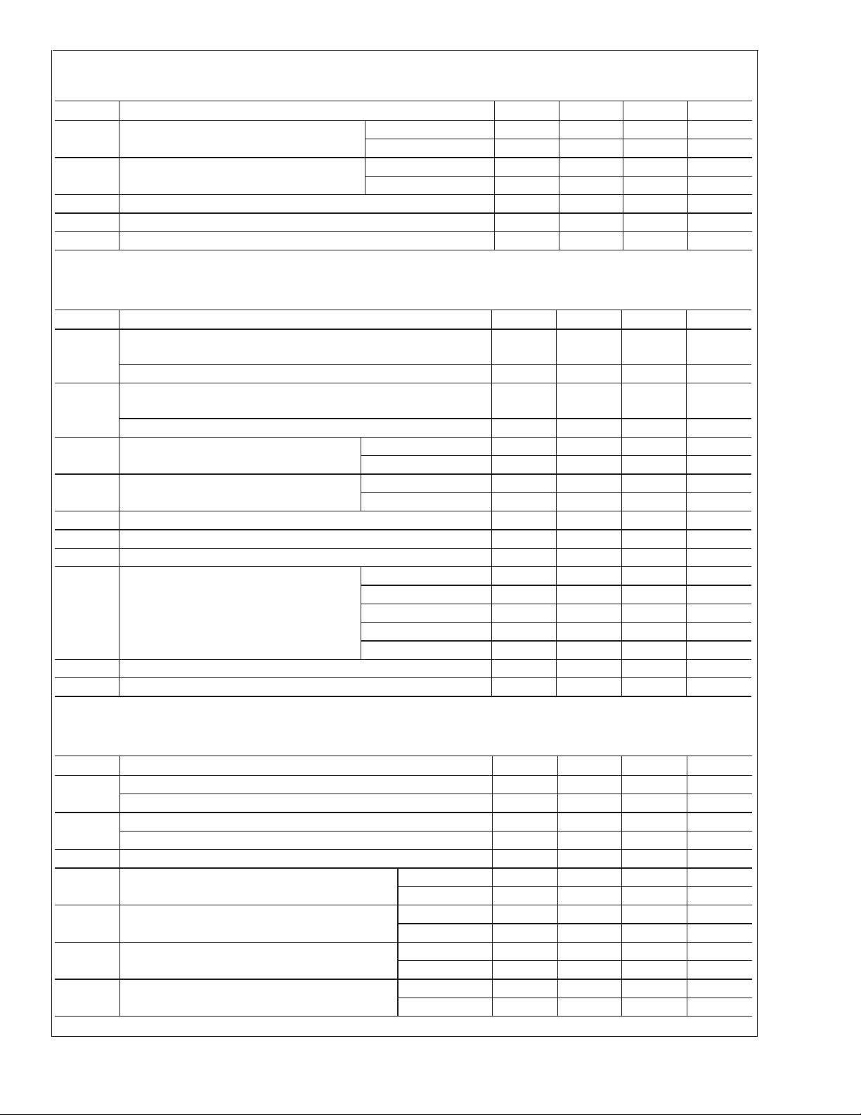
Electrical Characteristics
Over recommended operating supply and temperature ranges unless otherwise specified.
Symbol Parameter Conditions Min Typ Max Units
CMOS/TTL DC SPECIFICATIONS (Tx inputs, Rx outputs, control inputs and outputs)
V
IH
High Level Input Voltage 2.0 5.0 V
V
IL
Low Level Input Voltage GND 0.8 V
V
OH
High Level Output Voltage I
OH
= −0.4 mA 2.7 2.9 V
I
OH
= −2 mA 2.7 2.85 V
V
OL
Low Level Output Voltage I
OL
= 2 mA 0.1 0.3 V
V
CL
Input Clamp Voltage I
CL
= −18 mA −0.79 −1.5 V
I
IN
Input Current V
IN
= 0.4V, 2.5V or V
CC
+1.8 +15 µA
V
IN
= GND −15 0 µA
I
OS
Output Short Circuit Current V
OUT
= 0V −120 mA
LVDS DRIVER DC SPECIFICATIONS
V
OD
Differential Output Voltage R
L
= 100Ω 250 345 450 mV
∆V
OD
Change in V
OD
between
Complimentary Output States
35 mV
V
OS
Offset Voltage 1.125 1.25 1.375 V
∆V
OS
Change in V
OS
between
Complimentary Output States
35 mV
I
OS
Output Short Circuit Current V
OUT
= 0V, R
L
= 100Ω −3.5 −10 mA
I
OZ
Output TRI-STATE
®
Current PD = 0V, V
OUT
=0VorV
CC
±
1
±
10 µA
LVDS RECEIVER DC SPECIFICATIONS
V
TH
Differential Input High Threshold V
CM
= +1.2V +100 mV
V
TL
Differential Input Low Threshold −100 mV
I
IN
Input Current V
IN
= +2.4V, V
CC
= 3.6V
±
10 µA
V
IN
= 0V, V
CC
= 3.6V
±
10 µA
DS90C387/DS90CF388
www.national.com3
Electrical Characteristics (Continued)
Over recommended operating supply and temperature ranges unless otherwise specified.
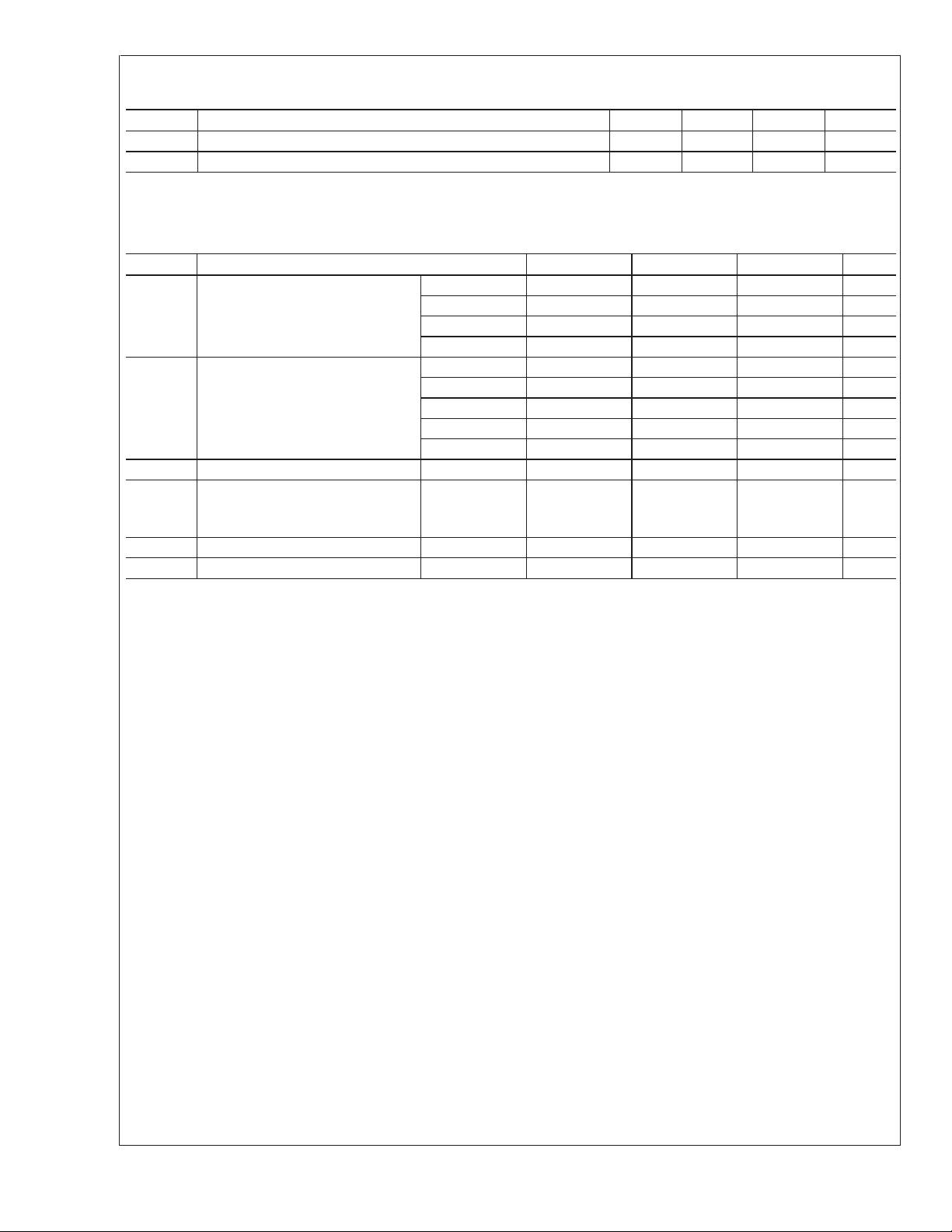
Symbol Parameter Conditions Min Typ Max Units
TRANSMITTER SUPPLY CURRENT
ICCTW Transmitter Supply Current
Worst Case
R
L
= 100Ω,C
L
=5
pF,
Worst Case
Pattern
(Figures 1, 3)
, DUAL=High
(48-bit RGB),
BAL=High
(enabled)
f = 32.5 MHz 91.4 140 mA
f = 65 MHz 106 160 mA
f = 85 MHz 135 183 mA
f = 112 MHz 155 210 mA
ICCTG Transmitter Supply Current
16 Grayscale
R
L
= 100Ω,C
L
=5
pF,
16 Grayscale
Pattern
(Figures 2, 3)
, DUAL=High
(48-bit RGB),
BAL=High
(enabled)
f = 32.5 MHz 62.6 120 mA
f = 65 MHz 84.4 130 mA
f = 85 MHz 89.0 145 mA
f = 112 MHz 94.5 155 mA
ICCTZ Transmitter Supply Current
Power Down
PD = Low
4.8 50 µA
Driver Outputs in TRI-STATE under
Powerdown Mode
RECEIVER SUPPLY CURRENT
ICCRW Receiver Supply Current
Worst Case
C
L
= 8 pF,
Worst Case
Pattern
(Figures 1, 4)
, DUAL (48-bit
RGB), BAL=High
(enabled)
f = 40MHz 125 160 mA
f = 65 MHz 200 250 mA
f = 85 MHz 240 275 mA
f = 112 MHz 250 300 mA
ICCRG Receiver Support Current
16 Grayscale
C
L
= 8 pF,
16 Grayscale
Pattern
(Figures 2, 4)
, DUAL (48-bit
RGB), BAL=High
(enabled)
f = 40MHz 60 95 mA
f = 65 MHz 95 125 mA
f = 85 MHz 115 150 mA
f = 112 MHz 150 270 mA
ICCRZ Receiver Supply Current
Power Down
PD = Low
Receiver Outputs stay low
during Powerdown mode.
255 300 µA
Note 1: “Absolute Maximum Ratings” are those values beyond which the safety of the device cannot be guaranteed. They are not meant to imply that the device
should be operated at these limits. The tables of “Electrical Characteristics” specify conditions for device operation.
Note 2: Typical values are given for V
CC
= 3.3V and T
A
= +25˚C.
Note 3: Current into device pins is defined as positive. Current out of device pins is defined as negative. Voltages are referenced to ground unless otherwise
specified (except V
OD
and ∆V
OD
).
DS90C387/DS90CF388
www.national.com 4
Recommended Transmitter Input Characteristics
Over recommended operating supply and temperature ranges unless otherwise specified.
Symbol Parameter Min Typ Max Units
TCIT TxCLK IN Transition Time (Figure 5) DUAL=Gnd or Vcc 1.0 2.0 3.0 ns
DUAL=1/2Vcc 1.0 1.5 1.7 ns
TCIP TxCLK IN Period (Figure 6) DUAL=Gnd or Vcc 8.928 T 30.77 ns
DUAL=1/2Vcc 5.88 15.38 ns
TCIH TxCLK in High Time (Figure 6) 0.35T 0.5T 0.65T ns
TCIL TxCLK in Low Time (Figure 6) 0.35T 0.5T 0.65T ns
TXIT TxIN Transition Time 1.5 6.0 ns
Transmitter Switching Characteristics
Over recommended operating supply and temperature ranges unless otherwise specified.
Symbol Parameter Min Typ Max Units
LLHT LVDS Low-to-High Transition Time (Figure 3), PRE = 0.75V
(disabled)
0.14 0.7 ns
LVDS Low-to-High Transition Time (Figure 3), PRE = Vcc (max) 0.11 0.6 ns
LHLT LVDS High-to-Low Transition Time (Figure 3), PRE = 0.75V
(disabled)
0.16 0.8 ns
LVDS High-to-Low Transition Time (Figure 3), PRE = Vcc (max) 0.11 0.7 ns
TBIT Transmitter Output Bit Width DUAL=Gnd or Vcc 1/7 TCIP ns
DUAL=1/2Vcc 2/7 TCIP ns
TPPOS Transmitter Pulse Positions - Normalized f = 33 to 70 MHz −250 0 +250 ps
f = 70 to 112 MHz −200 0 +200 ps
TCCS TxOUT Channel to Channel Skew 100 ps
TSTC TxIN Setup to TxCLK IN (Figure 6) 2.7 ns
THTC TxIN Hold to TxCLK IN (Figure 6)0ns
TJCC Transmitter Jitter Cycle-to-cycle (Figures
14, 15) (Note 5), DUAL=Vcc
f = 112 MHz 85 100 ps
f = 85 MHz 60 75 ps
f = 65 MHz 70 80 ps
f = 56 MHz 100 120 ps
f = 32.5 MHz 75 110 ps
TPLLS Transmitter Phase Lock Loop Set (Figure 8)10ms
TPDD Transmitter Powerdown Delay (Figure 10) 100 ns
Receiver Switching Characteristics
Over recommended operating supply and temperature ranges unless otherwise specified.
Symbol Parameter Min Typ Max Units
CLHT CMOS/TTL Low-to-High Transition Time (Figure 4), Rx data out 1.52 2.0 ns
CMOS/TTL Low-to-High Transition Time (Figure 4), Rx clock out 0.5 1.0 ns
CHLT CMOS/TTL High-to-Low Transition Time (Figure 4), Rx data out 1.7 2.0 ns
CMOS/TTL High-to-Low Transition Time (Figure 4), Rx clock out 0.5 1.0 ns
RCOP RxCLK OUT Period (Figure 7) 8.928 T 25 ns
RCOH RxCLK OUT High Time (Figure 7)(Note 4) f = 112 MHz 3.5 ns
f = 85 MHz 4.5 ns
RCOL RxCLK OUT Low Time (Figure 7)(Note 4) f = 112 MHz 3.5 ns
f = 85 MHz 4.5 ns
RSRC RxOUT Setup to RxCLK OUT (Figure 7)(Note 4) f = 112 MHz 2.4 ns
f = 85 MHz 3.0 ns
RHRC RxOUT Hold to RxCLK OUT (Figure 7)(Note 4) f = 112 MHz 3.4 ns
f = 85 MHz 4.75 ns
DS90C387/DS90CF388
www.national.com5
Receiver Switching Characteristics (Continued)
Over recommended operating supply and temperature ranges unless otherwise specified.
Symbol Parameter Min Typ Max Units
RPLLS Receiver Phase Lock Loop Set (Figure 9)10ms
RPDD Receiver Powerdown Delay (Figure 11)1µs
Chipset RSKM Characteristics
Over recommended operating supply and temperature ranges unless otherwise specified.(Notes 4, 8). See Applications Infor-
mation section for more details on this parameter and how to apply it.
Symbol Parameter Min Typ Max Units
RSKM Receiver Skew Margin without
Deskew in non-DC Balance Mode,
(Figure 12), (Note 6)
f = 112 MHz 170 ps
f = 100 MHz 170 240 ps
f = 85MHz 300 350 ps
f = 66MHz 300 350 ps
RSKM Receiver Skew Margin without
Deskew in DC Balance Mode,
(Figure 12), (Note 6)
f = 112 MHz 170 ps
f = 100 MHz 170 200 ps
f = 85 MHz 250 300 ps
f = 66 MHz 250 300 ps
f = 50MHz 100 350 ps
f = 40MHz 94 530 ps
RSKMD Receiver Skew Margin with Deskew
in DC Balance, (Figure 13),
(Note 7)
f=40to80
MHz
0.25TBIT ps
RDR Receiver Deskew Range f = 80 MHz
±
1 TBIT
RDSS Receiver Deskew Step Size f = 80 MHz 0.3 TBIT ns
Note 4: The Minimum and Maximum Limits are based on statistical analysis of the device performance over voltage and temperature ranges. This parameter is
functionally tested on Automatic Test Equipment (ATE). ATE is limited to 85MHz. A sample of characterization parts have been bench tested to verify functional
performance.
Note 5: The limits are based on bench characterization of the device’s jitter response over the power supply voltage range. Output clock jitter is measured with a
cycle-to-cycle jitter of
±
3ns applied to the input clock signal while data inputs are switching (see figures 15 and 16).A jitter event of 3ns, represents worse case jump
in the clock edge from most graphics VGA chips currently available. This parameter is used when calculating system margin as described in AN-1059.
Note 6: Receiver Skew Margin (RSKM) is defined as the valid data sampling region at the receiver inputs. This margin takes into account transmitter output pulse
positions (min and max) and the receiver input setup and hold time (internal data sampling window - RSPOS). This margin allows for LVDS interconnect skew,
inter-symbol interference (both dependent on type/length of cable) and clock jitter.
RSKM ≥ cable skew (type, length) + source clock jitter (cycle to cycle, TJCC) + ISI (if any). See Applications Information section for more details.
Note 7: Receiver Skew Margin with Deskew (RSKMD) is defined as the valid data sampling region at the receiver inputs. The DESKEW function will constrain the
receiver’s sampling strobes to the middle half of the LVDS bit and removes (adjusts for) fixed interconnect skew. This margin (RSKMD) allows for inter-symbol
interference (dependent on type/length of cable), Transmitter Pulse Position (TPPOS) variance, and LVDS clock jitter (TJCC).
RSKMD ≥ ISI + TPPOS(variance) + source clock jitter (cycle to cycle). See Applications Information section for more details.
Note 8: Typical values for RSKM and RSKMD are applicable for fixed V
CC
and T
A
for the Transmitter and Receiver (both are assumed to be at the same V
CC
and
T
A
points).
DS90C387/DS90CF388
www.national.com 6
AC Timing Diagrams
Note 9: The worst case test pattern produces a maximum toggling of digital circuits, LVDS I/O and CMOS/TTL I/O.
Note 10: The 16 grayscale test pattern tests device power consumption for a “typical” LCD display pattern. The test pattern approximates signal switching needed
to produce groups of 16 vertical stripes across the display.
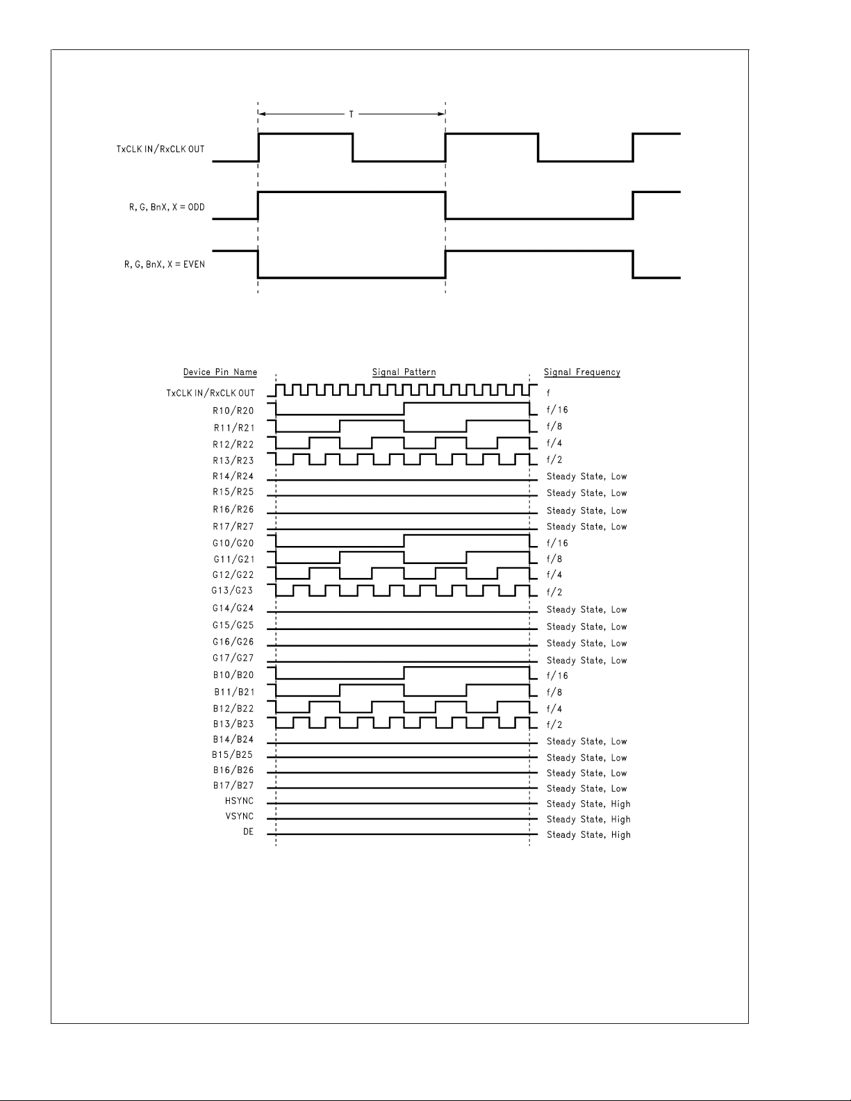
Note 11: Figures 1, 2 show a falling edge data strobe (TxCLK IN/RxCLK OUT).
10007310
FIGURE 1. “Worst Case” Test Pattern
10007311
FIGURE 2. “16 Grayscale” Test Pattern (Notes 9, 10, 11)
DS90C387/DS90CF388
www.national.com7
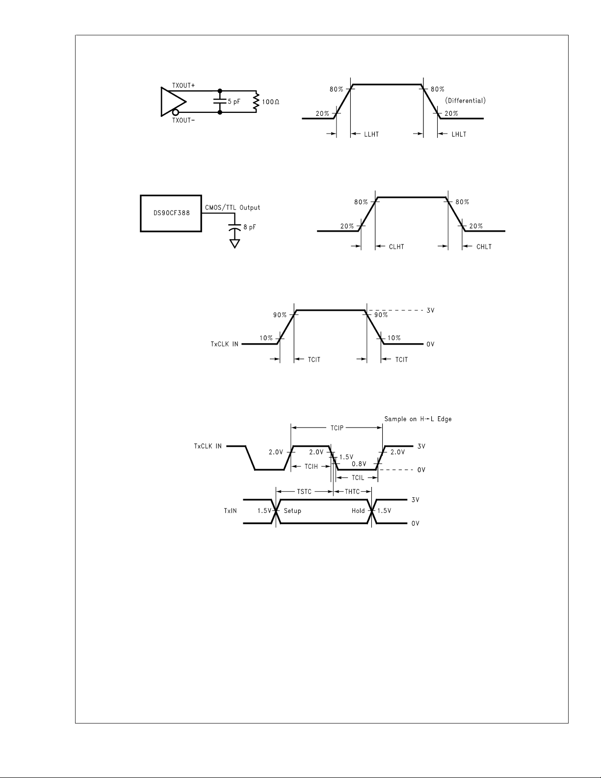
AC Timing Diagrams (Continued)
10007312
FIGURE 3. DS90C387 (Transmitter) LVDS Output Load and Transition Times
10007313
FIGURE 4. DS90CF388 (Receiver) CMOS/TTL Output Load and Transition Times
10007314
FIGURE 5. DS90C387 (Transmitter) Input Clock Transition Time
10007315
FIGURE 6. DS90C387 (Transmitter) Setup/Hold and High/Low Times (Falling Edge Strobe)
DS90C387/DS90CF388
www.national.com 8
 Loading...