


March 2005
LP2952/LP2952A/LP2953/LP2953A
Adjustable Micropower Low-Dropout Voltage Regulators
General Description
The LP2952 and LP2953 are micropower voltage regulators with very low quiescent current (130 µA typical at 1 mA load) and very low dropout voltage (typ. 60 mV at light load and 470 mV at 250 mA load current). They are ideally suited for battery-powered systems. Furthermore, the quiescent current increases only slightly at dropout, which prolongs battery life.
The LP2952 and LP2953 retain all the desirable characteristics of the LP2951, but offer increased output current, additional features, and an improved shutdown function.
The internal crowbar pulls the output down quickly when the shutdown is activated.
The error flag goes low if the output voltage drops out of regulation.
Reverse battery protection is provided.
The internal voltage reference is made available for external use, providing a low-T.C. reference with very good line and load regulation.
The parts are available in DIP and surface mount packages.
Features
n Output voltage adjusts from 1.23V to 29V n Guaranteed 250 mA output current
n Extremely low quiescent current n Low dropout voltage
n Extremely tight line and load regulation n Very low temperature coefficient
n Current and thermal limiting n Reverse battery protection
n 50 mA (typical) output pulldown crowbar n 5V and 3.3V versions available
LP2953 Versions Only
nAuxiliary comparator included with CMOS/TTL compatible output levels. Can be used for fault detection, low input line detection, etc.
Applications
n High-efficiency linear regulator
n Regulator with under-voltage shutdown n Low dropout battery-powered regulator n Snap-ON/Snap-OFF regulator
Block Diagrams
LP2952 |
LP2953 |
01112702
01112701
Regulators Voltage Dropout-Low Micropower Adjustable LP2952/LP2952A/LP2953/LP2953A
© 2005 National Semiconductor Corporation |
DS011127 |
www.national.com |
LP2952/LP2952A/LP2953/LP2953A
Pinout Drawings
LP2952
14-Pin DIP
01112711
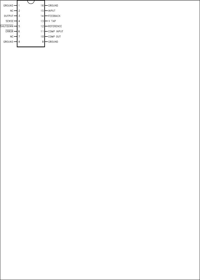
LP2953
16-Pin DIP
01112713
LP2952
16-Pin SO
01112712
LP2953
16-Pin SO
01112714
Ordering Information
LP2952
Order |
Temp. |
|
Package |
|
NSC |
|
Range |
|
|
|
Drawing |
||
Number |
|
|
|
|||
(TJ) ûC |
|
|
|
Number |
||
|
|
|
|
|
||
LP2952IN, |
−40 to |
|
14-Pin |
|
N14A |
|
LP2952AIN, |
+125 |
|
Molded |
|
|
|
LP2952IN-3.3, |
|
|
DIP |
|
|
|
LP2952AIN-3.3 |
|
|
|
|
|
|
|
|
|
|
|
|
|
LP2952IM, |
−40 to |
|
16-Pin |
|
M16A |
|
LP2952AIM, |
+125 |
|
Surface |
|
|
|
LP2952IM-3.3, |
|
|
Mount |
|
|
|
LP2952AIM-3.3 |
|
|
|
|
|
|
|
|
|
|
|
|
|
|
|
LP2953 |
|
|
|
|
|
|
|
|
|
|
|
Order |
|
Temp. |
|
Package |
NSC |
|
|
Range |
|
|
|
Drawing |
|
Number |
|
|
|
|
||
|
(TJ) ûC |
|
|
|
Number |
|
|
|
|
|
|
||
LP2953IN, |
|
−40 to |
|
16-Pin |
N16A |
|
LP2953AIN, |
|
+125 |
Molded DIP |
|
||
LP2953IN-3.3, |
|
|
|
|
|
|
LP2953AIN-3.3 |
|
|
|
|
|
|
|
|
|
|
|
|
|
LP2953IM, |
|
−40 to |
|
16-Pin |
M16A |
|
LP2953AIM, |
|
+125 |
|
Surface |
|
|
LP2953IM-3.3, |
|
|
|
Mount |
|
|
LP2953AIM-3.3 |
|
|
|
|
|
|
|
|
|
|
|
|
|
LP2953AMJ/883 |
|
−55 to |
|
16-Pin |
|
|
5962-9233601MEA |
|
+150 |
Ceramic DIP |
J16A |
||
LP2953AMJ-QMLV |
|
|
|
|
|
|
|
|
|
|
|
|
|
5962-9233601VEA |
|
|
|
|
|
|
|
|
|
|
|
|
|
LP2953AMWG/883 |
|
−55 to |
|
16-Pin |
|
|
5962-9233601QXA |
|
+150 |
|
Ceramic |
WG16A |
|
LP2953AMWG-QMLV |
|
|
|
Surface |
||
|
|
|
|
|||
5962-9233601VXA |
|
|
|
Mount |
|
|
|
|
|
|
|
|
|
www.national.com |
2 |

Absolute Maximum Ratings (Note 1)
If Military/Aerospace specified devices are required, please contact the National Semiconductor Sales Office/ Distributors for availability and specifications.
Storage Temperature Range |
−65˚C ≤ TA ≤ |
|
+150˚C |
Operating Temperature Range |
|
LP2952I, LP2953I, LP2952AI, |
|
LP2953AI, LP2952I-3.3, |
|
LP2953I-3.3, LP2952AI-3.3, |
|
LP2953AI-3.3 |
−40˚C ≤ TJ ≤ +125˚C |
LP2953AM |
−55˚C ≤ TA ≤ |
|
+125˚C |
Lead Temp. (Soldering, 5 seconds) |
260˚C |
Power Dissipation (Note 2) |
Internally Limited |
Maximum Junction Temperature |
|
LP2952I, LP2953I, LP2952AI, |
|
LP2953AI, LP2952I-3.3, |
|
LP2953I-3.3, LP2952AI-3.3, |
|
LP2953AI-3.3 |
+125˚C |
LP2953AM |
+150˚C |
Input Supply Voltage |
−20V to +30V |
Feedback Input Voltage (Note 3) |
−0.3V to +5V |
Comparator Input Voltage (Note 4) |
−0.3V to +30V |
Shutdown Input Voltage (Note 4) |
−0.3V to +30V |
Comparator Output Voltage (Note |
|
4) |
−0.3V to +30V |
ESD Rating (Note 15) |
2 kV |
Electrical Characteristics Limits in standard typeface are for TJ = 25˚C, bold typeface applies over the full operating temperature range. Limits are guaranteed by production testing or correlation techniques using standard Statistical Quality Control (SQC) methods. Unless otherwise specified: VIN = VO(NOM) + 1V, IL = 1 mA, CL = 2.2 µF for 5V parts and 4.7µF for 3.3V parts. Feedback pin is tied to V Tap pin, Output pin is tied to Output Sense pin.
3.3V Versions
Symbol |
Parameter |
Conditions |
Typical |
LP2952AI-3.3, LP2953AI-3.3 |
LP2952I-3.3, LP2953I-3.3 |
Units |
||
|
|
|
|
|
|
|
|
|
|
|
|
|
Min |
Max |
Min |
Max |
|
|
|
|
|
|
|
|
|
|
VO |
Output Voltage |
|
3.3 |
3.284 |
3.317 |
3.267 |
3.333 |
V |
|
|
|
|
3.260 |
3.340 |
3.234 |
3.366 |
|
|
|
|
|
|
|
|
|
|
|
|
1 mA ≤ IL ≤ 250 mA |
3.3 |
3.254 |
3.346 |
3.221 |
3.379 |
|
5V Versions
Symbol |
Parameter |
Conditions |
Typical |
LP2952AI, LP2953AI, |
LP2952I, LP2953I |
Units |
||
|
|
|
|
LP2953AM (Note 17) |
|
|
|
|
|
|
|
|
|
|
|
|
|
|
|
|
|
Min |
Max |
Min |
Max |
|
|
|
|
|
|
|
|
|
|
VO |
Output Voltage |
|
5.0 |
4.975 |
5.025 |
4.950 |
5.050 |
V |
|
|
|
|
4.940 |
5.060 |
4.900 |
5.100 |
|
|
|
|
|
|
|
|
|
|
|
|
1 mA ≤ IL ≤ 250 mA |
5.0 |
4.930 |
5.070 |
4.880 |
5.120 |
|
All Voltage Options
Electrical Characteristics
Limits in standard typeface are for TJ = 25˚C, bold typeface applies over the full operating temperature range. Limits are guaranteed by production testing or correlation techniques using standard Statistical Quality Control (SQC) methods. Unless otherwise specified: VIN = VO(NOM) + 1V, IL = 1 mA, CL = 2.2 µF for 5V parts and 4.7µF for 3.3V parts. Feedback pin is tied to V Tap pin, Output pin is tied to Output Sense pin.
Symbol |
Parameter |
Conditions |
Typical |
LP2952AI, LP2953AI, |
LP2952I, LP2953I, |
Units |
||
|
|
|
|
LP2952AI-3.3, |
LP2952I-3.3, |
|
||
|
|
|
|
LP2953AI-3.3, |
LP2953I-3.3 |
|
||
|
|
|
|
LP2953AM |
|
|
|
|
|
|
|
|
(Notes 16, 17) |
|
|
|
|
|
|
|
|
|
|
|
|
|
|
|
|
|
Min |
Max |
Min |
Max |
|
|
|
|
|
|
|
|
|
|
REGULATOR |
|
|
|
|
|
|
|
|
|
|
|
|
|
|
|
|
|
|
Output Voltage Temp. |
(Note 5) |
20 |
|
100 |
|
150 |
ppm/˚C |
|
Coefficient |
|
|
|
|
|
|
|
|
|
|
|
|
|
|
|
|
|
Output Voltage Line |
VIN = VO(NOM) + 1V to 30V |
0.03 |
|
0.1 |
|
0.2 |
% |
|
Regulation |
|
|
|
0.2 |
|
0.4 |
|
|
|
|
|
|
|
|
||
|
|
|
|
|
|
|
|
|
LP2952/LP2952A/LP2953/LP2953A
3 |
www.national.com |

LP2952/LP2952A/LP2953/LP2953A
All Voltage Options (Continued)
Electrical Characteristics (Continued)
Limits in standard typeface are for TJ = 25˚C, bold typeface applies over the full operating temperature range. Limits are guaranteed by production testing or correlation techniques using standard Statistical Quality Control (SQC) methods. Unless otherwise specified: VIN = VO(NOM) + 1V, IL = 1 mA, CL = 2.2 µF for 5V parts and 4.7µF for 3.3V parts. Feedback pin is tied to V Tap pin, Output pin is tied to Output Sense pin.
Symbol |
Parameter |
Conditions |
Typical |
LP2952AI, LP2953AI, |
LP2952I, LP2953I, |
Units |
||
|
|
|
|
LP2952AI-3.3, |
LP2952I-3.3, |
|
||
|
|
|
|
LP2953AI-3.3, |
LP2953I-3.3 |
|
||
|
|
|
|
LP2953AM |
|
|
|
|
|
|
|
|
(Notes 16, 17) |
|
|
|
|
|
|
|
|
|
|
|
|
|
|
|
|
|
Min |
Max |
Min |
Max |
|
|
|
|
|
|
|
|
|
|
|
Output Voltage Load |
IL = 1 mA to 250 mA |
0.04 |
|
0.16 |
|
0.20 |
% |
|
Regulation (Note 6) |
IL = 0.1 mA to 1 mA |
|
|
0.20 |
|
0.30 |
|
|
|
|
|
|
|
|||
|
|
|
|
|
|
|
|
|
VIN–VO |
Dropout Voltage |
IL = 1 mA |
60 |
|
100 |
|
100 |
mV |
|
(Note 7) |
|
|
|
150 |
|
150 |
|
|
|
|
|
|
|
|
|
|
|
|
IL = 50 mA |
240 |
|
300 |
|
300 |
|
|
|
|
|
|
420 |
|
420 |
|
|
|
|
|
|
|
|
|
|
|
|
IL = 100 mA |
310 |
|
400 |
|
400 |
|
|
|
|
|
|
520 |
|
520 |
|
|
|
|
|
|
|
|
|
|
|
|
IL = 250 mA |
470 |
|
600 |
|
600 |
|
|
|
|
|
|
800 |
|
800 |
|
|
|
|
|
|
|
|
|
|
IGND |
Ground Pin Current |
IL = 1 mA |
130 |
|
170 |
|
170 |
µA |
|
(Note 8) |
|
|
|
200 |
|
200 |
|
|
|
|
|
|
|
|
|
|
|
|
IL = 50 mA |
1.1 |
|
2 |
|
2 |
mA |
|
|
|
|
|
2.5 |
|
2.5 |
|
|
|
|
|
|
|
|
|
|
|
|
IL = 100 mA |
4.5 |
|
6 |
|
6 |
|
|
|
|
|
|
8 |
|
8 |
|
|
|
|
|
|
|
|
|
|
|
|
IL = 250 mA |
21 |
|
28 |
|
28 |
|
|
|
|
|
|
33 |
|
33 |
|
|
|
|
|
|
|
|
|
|
IGND |
Ground Pin Current at |
VIN = VO(NOM) −0.5V |
165 |
|
210 |
|
210 |
µA |
|
Dropout |
IL = 100 µA |
|
|
240 |
|
240 |
|
IGND |
Ground Pin Current at |
VSHUTDOWN ≤ 1.1V |
105 |
|
140 |
|
140 |
µA |
|
Shutdown (Note 8) |
|
|
|
|
|
|
|
|
|
|
|
|
|
|
|
|
ILIMIT |
Current Limit |
VOUT = 0 |
380 |
|
500 |
|
500 |
mA |
|
|
|
|
|
530 |
|
530 |
|
|
|
|
|
|
|
|
|
|
|
Thermal Regulation |
(Note 10) |
0.05 |
|
0.2 |
|
0.2 |
%/W |
|
|
|
|
|
|
|
|
|
en |
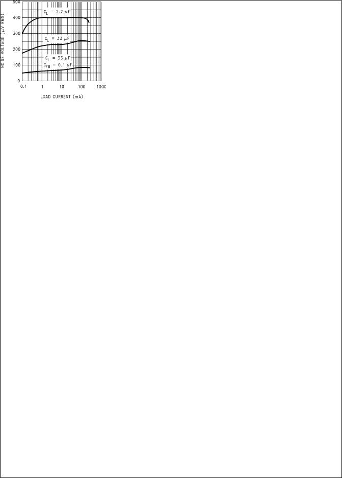
Output Noise Voltage |
CL = 4.7 µF |
400 |
|
|
|
|
µV |
|
(10 Hz to 100 kHz) |
CL = 33 µF |
260 |
|
|
|
|
RMS |
|
IL = 100 mA |
CL = 33 µF (Note 11) |
80 |
|
|
|
|
|
VREF |
Reference Voltage |
(Note 12) |
1.230 |
1.215 |
1.245 |
1.205 |
1.255 |
V |
|
|
|
|
1.205 |
1.255 |
1.190 |
1.270 |
|
|
|
|
|
|
|
|
|
|
|
Reference Voltage Line |
VIN = 2.5V to VO(NOM) + 1V |
0.03 |
|
0.1 |
|
0.2 |
% |
|
Regulation |
VIN = VO(NOM) + 1V to 30V |
|
|
0.2 |
|
0.4 |
|
|
|
(Note 13) |
|
|
|
|
|
|
|
|
|
|
|
|
|
|
|
|
Reference Voltage Load |
IREF = 0 to 200 µA |
0.25 |
|
0.4 |
|
0.8 |
% |
|
Regulation |
|
|
|
0.6 |
|
1.0 |
|
|
|
|
|
|
|
|
||
|
|
|
|
|
|
|
|
|
|
Reference Voltage |
(Note 5) |
20 |
|
|
|
|
ppm/˚C |
|
Temp. Coefficient |
|
|
|
|
|
|
|
|
|
|
|
|
|
|
|
|
www.national.com |
4 |

All Voltage Options (Continued)
Electrical Characteristics (Continued)
Limits in standard typeface are for TJ = 25˚C, bold typeface applies over the full operating temperature range. Limits are guaranteed by production testing or correlation techniques using standard Statistical Quality Control (SQC) methods. Unless otherwise specified: VIN = VO(NOM) + 1V, IL = 1 mA, CL = 2.2 µF for 5V parts and 4.7µF for 3.3V parts. Feedback pin is tied to V Tap pin, Output pin is tied to Output Sense pin.
|
Symbol |
|
Parameter |
Conditions |
Typical |
LP2952AI, LP2953AI, |
LP2952I, LP2953I, |
Units |
|||
|
|
|
|
|
|
|
LP2952AI-3.3, |
LP2952I-3.3, |
|
||
|
|
|
|
|
|
|
LP2953AI-3.3, |
LP2953I-3.3 |
|
||
|
|
|
|
|
|
|
LP2953AM |
|
|
|
|
|
|
|
|
|
|
|
(Notes 16, 17) |
|
|
|
|
|
|
|
|
|
|
|
|
|
|
|
|
|
|
|
|
|
|
|
Min |
Max |
Min |
Max |
|
|
|
|
|
|
|
|
|
|
|
|
|
IB(FB) |
Feedback Pin Bias |
|
|
20 |
|
40 |
|
40 |
nA |
||
|
|
Current |
|
|
|
|
60 |
|
60 |
|
|
|
|
|
|
|
|
|
|
|
|
|
|
IO(SINK) |
Output “OFF” Pulldown |
(Note 9) |
|
30 |
|
30 |
|
mA |
|||
|
|
Current |
|
|
|
20 |
|
20 |
|
|
|
|
|
|
|
|
|
|
|
|
|
|
|
DROPOUT DETECTION COMPARATOR |
|
|
|
|
|
|
|||||
|
|
|
|
|
|
|
|
|
|
|
|
IOH |
Output “HIGH” Leakage |
VOH = 30V |
0.01 |
|
1 |
|
1 |
µA |
|||
|
|
|
|
|
|
|
|
2 |
|
2 |
|
|
|
|
|
|
|
|
|
|
|
|
|
VOL |
Output “LOW” Voltage |
VIN = VO(NOM) − 0.5V |
150 |
|
250 |
|
250 |
mV |
|||
|
|
|
|
IO(COMP) = 400 µA |
|
|
400 |
|
400 |
|
|
VTHR |
Upper Threshold |
(Note 14) |
−60 |
−80 |
−35 |
−80 |
−35 |
mV |
|||
(MAX) |
Voltage |
|
|
|
−95 |
−25 |
−95 |
−25 |
|
||
|
|
|
|
|
|
|
|
|
|
|
|
VTHR |
Lower Threshold |
(Note 14) |
−85 |
−110 |
−55 |
−110 |
−55 |
mV |
|||
(MIN) |
Voltage |
|
|
|
−160 |
−40 |
−160 |
−40 |
|
||
|
|
|
|
|
|
|
|
|
|
|
|
HYST |
Hysteresis |
(Note 14) |
15 |
|
|
|
|
mV |
|||
|
|
|
|
|
|
|
|
|
|
|
|
|
|
INPUT (Note 15) |
|
|
|
|
|
|
|
|
|
SHUTDOWN |
|
|
|
|
|
|
|
|
|||
VOS |
Input Offset |
(Referred to VREF) |
±3 |
−7.5 |
7.5 |
−7.5 |
7.5 |
mV |
|||
|
|
Voltage |
|
|
|
−10 |
10 |
−10 |
10 |
|
|
|
|
|
|
|
|
|
|
|
|
|
|
HYST |
Hysteresis |
|
|
6 |
|
|
|
|
mV |
||
|
|
|
|
|
|
|
|
|
|
|
|
IB |
Input Bias |
VIN(S/D) = 0V to 5V |
10 |
−30 |
30 |
−30 |
−30 |
nA |
|||
|
|
Current |
|
|
|
−50 |
50 |
−50 |
50 |
|
|
|
|
|
|
|
|
|
|
|
|
|
|
|
|
|
|
|
LP2953AM |
10 |
−30 |
30 |
|
|
|
|
|
|
|
|
|
|
−75 |
75 |
|
|
|
|
|
|
|
|
|
|
|
|
|
|
|
AUXILIARY COMPARATOR (LP2953 Only) |
|
|
|
|
|
|
|||||
|
|
|
|
|
|
|
|
|
|
|
|
VOS |
Input Offset Voltage |
(Referred to VREF) |
±3 |
−7.5 |
7.5 |
−7.5 |
7.5 |
mV |
|||
|
|
|
|
|
|
|
−10 |
10 |
−10 |
10 |
|
|
|
|
|
|
|
|
|
|
|
|
|
|
|
|
|
|
LP2953AM |
±3 |
−7.5 |
7.5 |
|
|
|
|
|
|
|
|
|
|
−12 |
12 |
|
|
|
|
|
|
|
|
|
|
|
|
|
|
|
HYST |
Hysteresis |
|
|
6 |
|
|
|
|
mV |
||
|
|
|
|
|
|
|
|
|
|
|
|
IB |
Input Bias Current |
VIN(COMP) = 0V to 5V |
10 |
−30 |
30 |
−30 |
30 |
nA |
|||
|
|
|
|
|
|
|
−50 |
50 |
−50 |
50 |
|
|
|
|
|
|
|
|
|
|
|
|
|
|
|
|
|
|
LP2953AM |
10 |
−30 |
30 |
|
|
|
|
|
|
|
|
|
|
−75 |
75 |
|
|
|
|
|
|
|
|
|
|
|
|
|
|
|
IOH |
Output “HIGH” Leakage |
VOH = 30V |
0.01 |
|
1 |
|
1 |
µA |
|||
|
|
|
|
VIN(COMP) = 1.3V |
|
|
2 |
|
2 |
|
|
|
|
|
|
|
LP2953AM |
0.01 |
|
1 |
|
|
|
|
|
|
|
|
|
|
|
2.2 |
|
|
|
|
|
|
|
|
|
|
|
|
|
|
|
VOL |
Output “LOW” Voltage |
VIN(COMP) = 1.1V |
150 |
|
250 |
|
250 |
mV |
|||
|
|
|
|
IO(COMP) = 400 µA |
|
|
400 |
|
400 |
|
|
|
|
|
|
|
LP2953AM |
150 |
|
250 |
|
|
|
|
|
|
|
|
|
|
|
420 |
|
|
|
|
|
|
|
|
|
|
|
|
|
|
|
LP2952/LP2952A/LP2953/LP2953A
5 |
www.national.com |
LP2952/LP2952A/LP2953/LP2953A
All Voltage Options (Continued)
Electrical Characteristics (Continued)
Note 1: Absolute maximum ratings indicate limits beyond which damage to the component may occur. Electrical specifications do not apply when operating the device outside of its rated operating conditions.
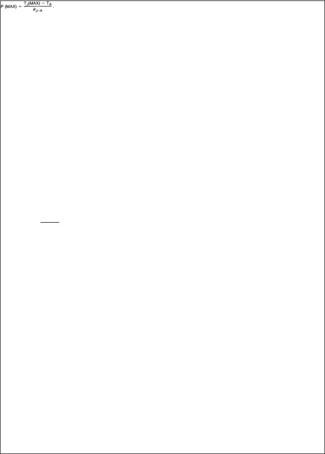
Note 2: The maximum allowable power dissipation is a function of the maximum junction temperature, TJ(MAX), the junction-to-ambient thermal resistance, θJ–A, and the ambient temperature, TA. The maximum allowable power dissipation at any ambient temperature is calculated using the equation for P(MAX),
.
Exceeding the maximum allowable power dissipation will cause excessive die temperature, and the regulator will go into thermal shutdown. See APPLICATION HINTS for additional information on heatsinking and thermal resistance.
Note 3: When used in dual-supply systems where the regulator load is returned to a negative supply, the output voltage must be diode-clamped to ground.
Note 4: May exceed the input supply voltage.
Note 5: Output or reference voltage temperature coefficient is defined as the worst case voltage change divided by the total temperature range.
Note 6: Load regulation is measured at constant junction temperature using low duty cycle pulse testing. Two separate tests are performed, one for the range of 100 µA to 1 mA and one for the 1 mA to 250 mA range. Changes in output voltage due to heating effects are covered by the thermal regulation specification.
Note 7: Dropout voltage is defined as the input to output differential at which the output voltage drops 100 mV below the value measured with a 1V differential. At very low values of programmed output voltage, the input voltage minimum of 2V (2.3V over temperature) must be observed.
Note 8: Ground pin current is the regulator quiescent current. The total current drawn from the source is the sum of the ground pin current, output load current, and current through the external resistive divider (if used).
Note 9: VSHUTDOWN ≤ 1.1V, VOUT = VO(NOM).
Note 10: Thermal regulation is the change in output voltage at a time T after a change in power dissipation, excluding load or line regulation effects. Specifications are for a 200 mA load pulse at VIN = VO(NOM)+15V (3W pulse) for T = 10 ms.
Note 11: Connect a 0.1 µF capacitor from the output to the feedback pin. Note 12: VREF ≤ VOUT ≤ (VIN − 1V), 2.3V ≤ VIN ≤ 30V, 100 µA ≤ IL ≤ 250 mA.
Note 13: Two separate tests are performed, one covering 2.5V ≤ VIN ≤ VO(NOM)+1V and the other test for VO(NOM)+1V ≤ VIN ≤ 30V.
Note 14: Comparator thresholds are expressed in terms of a voltage differential at the Feedback terminal below the nominal reference voltage measured atVIN = VO(NOM) + 1V. To express these thresholds in terms of output voltage change, multiply by the Error amplifier gain, which is VOUT/VREF = (R1 + R2)/R2(refer to
Figure 4).
Note 15: Human body model, 200 pF discharged through 1.5 kΩ.
Note 16: Drive Shutdown pin with TTL or CMOS-low level to shut regulator OFF, high level to turn regulator ON.
Note 17: A military RETS specification is available upon request. For more information on military products, please refer to the Mil-Aero web page at http://www.national.com/appinfo/milaero/index.html.
www.national.com |
6 |
Typical Performance Characteristics
Unless otherwise specified: VIN = 6V, IL = 1 mA, CL = 2.2 µF, VSD = 3V, TA = 25˚C, VOUT = 5V.
Quiescent Current
01112727
Ground Pin Current vs Load
01112729
Ground Pin Current
01112731
Quiescent Current
01112728
Ground Pin Current
01112730
Output Noise Voltage
01112732
LP2952/LP2952A/LP2953/LP2953A
7 |
www.national.com |
 Loading...