


LMP7707
Table of contents
 Loading...
July 30, 2008
LMP7707/LMP7708/LMP7709
Precision, CMOS Input, RRIO, Wide Supply Range
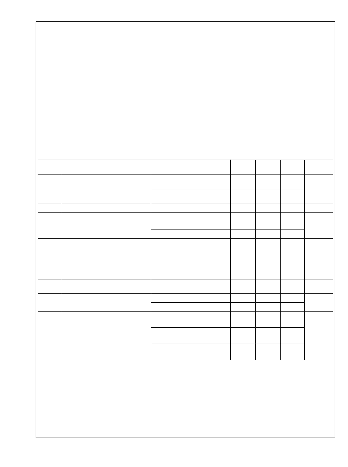
Decompensated Amplifiers
General Description
The LMP7707/LMP7708/LMP7709 devices are single, dual,
and quad low offset voltage, rail-to-rail input and output pre-
cision amplifiers which each have a CMOS input stage and a
wide supply voltage range. The LMP7707/LMP7708/
LMP7709 are part of the LMP
®
precision amplifier family and
are ideal for sensor interface and other instrumentation ap-
plications. These decompensated amplifiers are stable at a
gain of 6 and higher.
The guaranteed low offset voltage of less than ±200 µV along
with the guaranteed low input bias current of less than ±1 pA
make the LMP7707/LMP7708/LMP7709 ideal for precision
applications. The LMP7707/LMP7708/LMP7709 are built uti-
lizing VIP50 technology, which allows the combination of a
CMOS input stage and a supply voltage range of 12V with
rail-to-rail common mode voltage capability. The LMP7707/
LMP7708/LMP7709 are the perfect choice in many applica-
tions where conventional CMOS parts cannot operate due to
the voltage conditions.
The unique design of the rail-to-rail input stage of each of the
LMP7707/LMP7708/LMP7709 significantly reduces the CM-
RR glitch commonly associated with rail-to-rail input ampli-
fiers. Both sides of the complimentary input stage have been
trimmed, thereby reducing the difference between the NMOS
and PMOS offsets. The output swings within 40 mV of either
rail to maximize the signal dynamic range in applications re-
quiring low supply voltage.
The LMP7707 is offered in the space saving 5-Pin SOT23 and
8-pin SOIC package, the LMP7708 is offered in the 8-Pin
MSOP and 8-pin SOIC package and the quad LMP7709 is
offered in the 14-Pin TSSOP and the 14-pin SOIC package.
These small packages are ideal solutions for area con-
strained PC boards and portable electronics.
Features
Unless otherwise noted, typical values at V
S
= 5V.
■
Input offset voltage (LMP7707) ±200 µV (max)
■
Input offset voltage (LMP7708/LMP7709) ±220 µV (max)
■
Input bias current ±200 fA
■
Input voltage noise 9 nV/√Hz
■
CMRR 130 dB
■
Open loop gain 130 dB
■
Temperature range −40°C to 125°C
■
Gain bandwidth product (A
V
=10) 14 MHz
■
Stable at a gain of 10 or higher
■
Supply current (LMP7707) 715 µA
■
Supply current (LMP7708) 1.5 mA
■
Supply current (LMP7709) 2.9 mA
■
Supply voltage range 2.7V to 12V
■
Rail-to-rail input and output
Applications
■
High impedance sensor interface
■
Battery powered instrumentation
■
High gain amplifiers
■
DAC buffer
■
Instrumentation amplifier
■
Active filters
Open Loop Frequency Response
20203764
Increased Bandwidth for Same Supply Current at A
V
> 10
LMP
®
is a registered trademark of National Semiconductor Corporation.
© 2008 National Semiconductor Corporation 202037 www.national.com
LMP7707/LMP7708/LMP7709 Precision, CMOS Input, RRIO, Wide Supply Range Decompensated
Amplifiers
Absolute Maximum Ratings (Note 1)
If Military/Aerospace specified devices are required,
please contact the National Semiconductor Sales Office/
Distributors for availability and specifications.
ESD Tolerance (Note 2)
Human Body Model 2000V
Machine Model 200V
Charge Device Model 1000V
V
IN
Differential
±300 mV
Supply Voltage (V
S
= V
+
– V
−
)
13.2V
Voltage at Input/Output Pins V
+
+ 0.3V to V
−
− 0.3V
Input Current 10 mA
Storage Temperature Range −65°C to +150°C
Junction Temperature (Note 3) +150°C
Soldering Information
Infrared or Convection (20 sec) 235°C
Wave Soldering Lead Temp. (10
sec) 260°C
Operating Ratings (Note 1)
Temperature Range (Note 3) −40°C to +125°C
Supply Voltage (V
S
= V
+
– V
−
)
2.7V to 12V
Package Thermal Resistance (θ
JA
) (Note 3)
5-Pin SOT23 265°C/W
8-Pin SOIC 190°C/W
8-Pin MSOP 235°C/W
14-Pin TSSOP 122°C/W
14-Pin SOIC 145°C/W
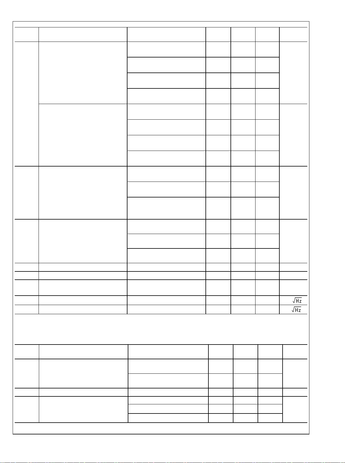
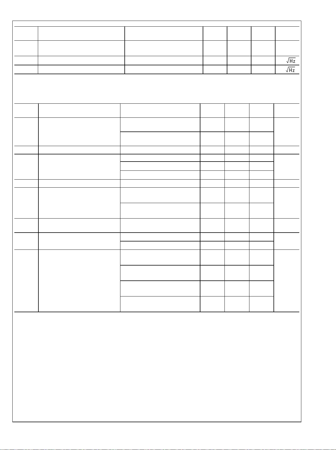
3V Electrical Characteristics (Note 4)
Unless otherwise specified, all limits are guaranteed for T
A
= 25°C, V
+
= 3V, V
−
= 0V, V
CM
= V
+
/2, and R
L
> 10 kΩ to V
+
/2.
Boldface limits apply at the temperature extremes.
Symbol Parameter Conditions Min
(Note 6)
Typ
(Note 5)
Max
(Note 6)
Units
V
OS
Input Offset Voltage LMP7707 ±37 ±200
±500
μV
LMP7708/LMP7709 ±56 ±220
±520
TCV
OS
Input Offset Voltage Drift (Note 7) ±1 ±5
μV/°C
I
B
Input Bias Current (Notes 7, 8) ±0.2 ±1
pA
−40°C ≤ T
A
≤ 85°C
±50
−40°C ≤ T
A
≤ 125°C
±400
I
OS
Input Offset Current 40 fA
CMRR Common Mode Rejection Ratio
0V ≤ V
CM
≤ 3V
LMP7707
86
80
130
dB
0V ≤ V
CM
≤ 3V
LMP7708/LMP7709
84
78
130
PSRR Power Supply Rejection Ratio
2.7V ≤ V
+
≤ 12V, V
O
= V
+
/2
86
82
98
dB
CMVR Input Common-Mode Voltage Range
CMRR ≥ 80 dB
−0.2 3.2
V
CMRR ≥ 77 dB
−0.2 3.2
A
VOL
Open Loop Voltage Gain
R
L
= 2 kΩ (LMP7707)
V
O
= 0.3V to 2.7V
100
96
114
dB
R
L
= 2 kΩ (LMP7708/LMP7709)
V
O
= 0.3V to 2.7V
100
94
114
R
L
= 10 kΩ
V
O
= 0.2V to 2.8V
100
96
124
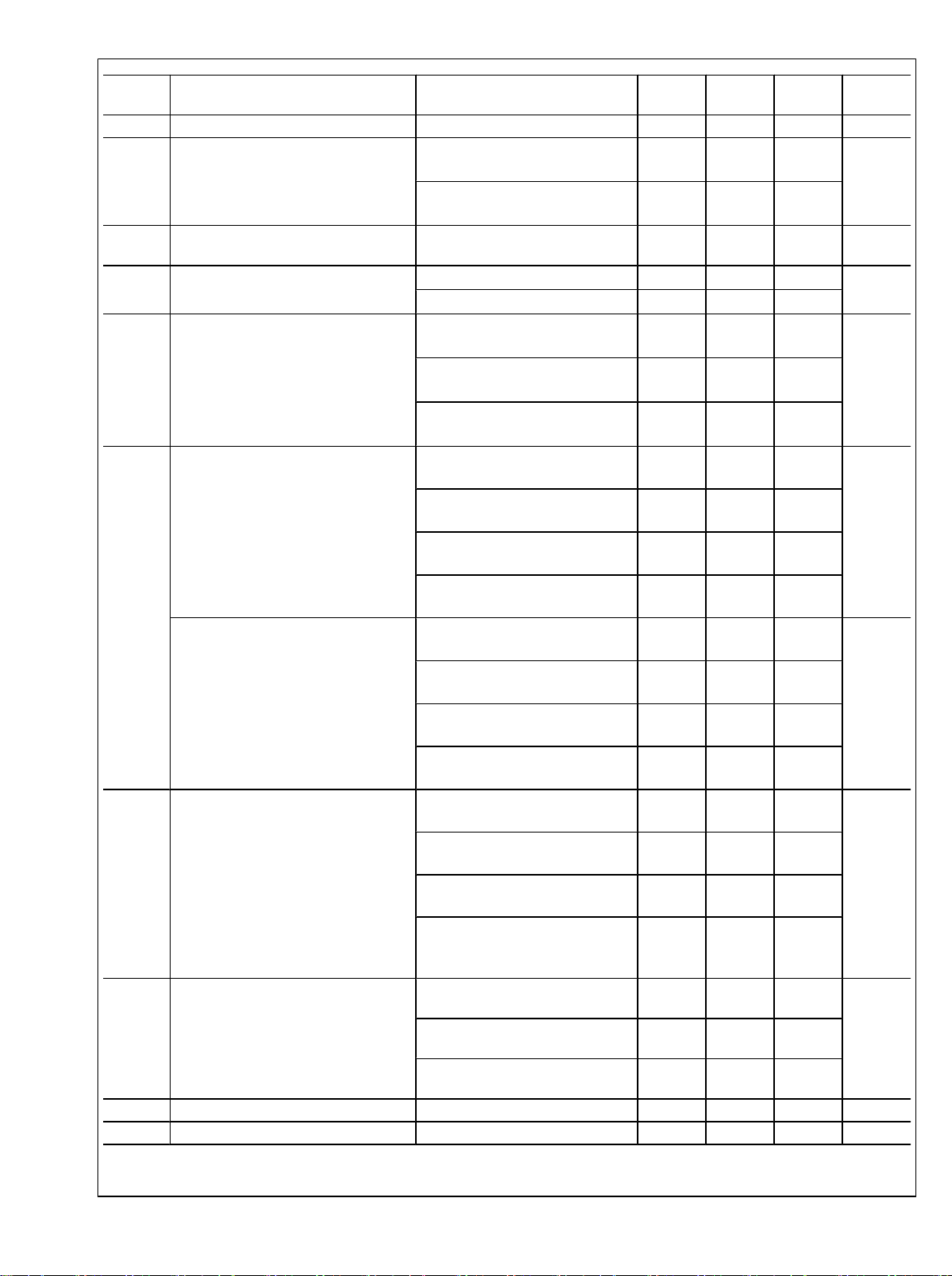
www.national.com 2
LMP7707/LMP7708/LMP7709
Symbol Parameter Conditions Min
(Note 6)
Typ
(Note 5)
Max
(Note 6)
Units
V
O
Output Swing High
R
L
= 2 kΩ to V
+
/2
LMP7707
40 80
120
mV
from V
+
R
L
= 2 kΩ to V
+
/2
LMP7708/LMP7709
40 80
150
R
L
= 10 kΩ to V
+
/2
LMP7707
30 40
60
R
L
= 10 kΩ to V
+
/2
LMP7708/LMP7709
35 50
100
Output Swing Low
R
L
= 2 kΩ to V
+
/2
LMP7707
40 60
80
mV
R
L
= 2 kΩ to V
+
/2
LMP7708/LMP7709
45 100
170
R
L
= 10 kΩ to V
+
/2
LMP7707
20 40
50
R
L
= 10 kΩ to V
+
/2
LMP7708/LMP7709
20 50
90
I
O
Output Short Circuit Current
(Notes 3, 9)
Sourcing V
O
= V
+
/2
V
IN
= 100 mV
25
15
42
mA
Sinking V
O
= V
+
/2
V
IN
= −100 mV (LMP7707)
25
20
42
Sinking V
O
= V
+
/2
V
IN
= −100 mV (LMP7708/
LMP7709)
25
15
42
I
S
Supply Current LMP7707 0.670 1.0
1.2
mA
LMP7708 1.4 1.8
2.1
LMP7709 2.9 3.5
4.5
SR Slew Rate (Note 10) V
O
= 2 V
PP,
10% to 90% 5.1
V/μs
GBWP Gain Bandwidth Product A
V
= 10 13 MHz
THD+N Total Harmonic Distortion + Noise f = 1 kHz, A
V
= 10, V
O
= 2.5V,
R
L
= 10 kΩ
0.024 %
e
n
Input-Referred Voltage Noise f = 1 kHz 9
nV/
i
n
Input-Referred Current Noise f = 100 kHz 1
fA/
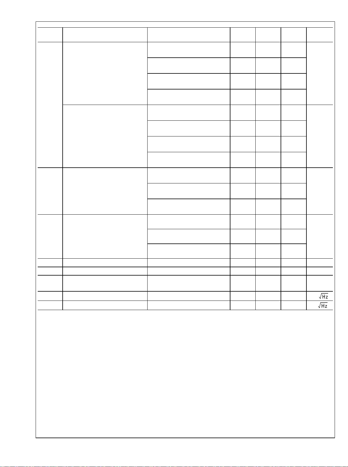
5V Electrical Characteristics (Note 4)
Unless otherwise specified, all limits are guaranteed for T
A
= 25°C, V
+
= 5V, V
−
= 0V, V
CM
= V
+
/2, and R
L
> 10 kΩ to V
+
/2.
Boldface limits apply at the temperature extremes.
Symbol Parameter Conditions Min
(Note 6)
Typ
(Note 5)
Max
(Note 6)
Units
V
OS
Input Offset Voltage LMP7707 ±37 ±200
±500
μV
LMP7708/LMP7709 ±32 ±220
±520
TCV
OS
Input Offset Voltage Drift (Note 7) ±1 ±5
μV/°C
I
B
Input Bias Current (Notes 7, 8) ±0.2 ±1
pA
−40°C ≤ T
A
≤ 85°C
±50
−40°C ≤ T
A
≤ 125°C
±400
3 www.national.com
LMP7707/LMP7708/LMP7709
Symbol Parameter Conditions Min
(Note 6)
Typ
(Note 5)
Max
(Note 6)
Units
I
OS
Input Offset Current 40
fA
CMRR Common Mode Rejection Ratio
0V ≤ V
CM
≤ 5V
LMP7707
88
83
130
dB
0V ≤ V
CM
≤ 5V
LMP7708/LMP7709
86
81
130
PSRR Power Supply Rejection Ratio
2.7V ≤ V
+
≤ 12V, V
O
= V
+
/2
86
82
100
dB
CMVR Input Common-Mode Voltage Range
CMRR ≥ 80 dB
−0.2 5.2
V
CMRR ≥ 78 dB
−0.2 5.2
A
VOL
Open Loop Voltage Gain
R
L
= 2 kΩ (LMP7707)
V
O
= 0.3V to 4.7V
100
96
119
dB
R
L
= 2 kΩ (LMP7708/LMP7709)
V
O
= 0.3V to 4.7V
100
94
119
R
L
= 10 kΩ
V
O
= 0.2V to 4.8V
100
96
130
V
O
Output Swing High
R
L
= 2 kΩ to V
+
/2
LMP7707
60 110
130
mV
from V
+
R
L
= 2 kΩ to V
+
/2
LMP7708/LMP7709
60 120
200
R
L
= 10 kΩ to V
+
/2
LMP7707
40 50
70
R
L
= 10 kΩ to V
+
/2
LMP7708/LMP7709
40 60
120
Output Swing Low
R
L
= 2 kΩ to V
+
/2
LMP7707
50 80
90
mV
R
L
= 2 kΩ to V
+
/2
LMP7708/LMP7709
50 120
190
R
L
= 10 kΩ to V
+
/2
LMP7707
30 40
50
R
L
= 10 kΩ to V
+
/2
LMP7708/LMP7709
30 50
100
I
O
Output Short Circuit Current
(Notes 3, 9)
Sourcing V
O
= V
+
/2
V
IN
= 100 mV (LMP7707)
40
28
66
mA
Sourcing V
O
= V
+
/2
V
IN
= 100 mV (LMP7708/LMP7709)
38
25
66
Sinking V
O
= V
+
/2
V
IN
= −100 mV (LMP7707)
40
28
76
Sinking V
O
= V
+
/2
V
IN
= −100 mV (LMP7708/
LMP7709)
40
23
76
I
S
Supply Current LMP7707 0.715 1.0
1.2
mA
LMP7708 1.5 1.9
2.2
LMP7709 2.9 3.7
4.6
SR Slew Rate (Note 10) V
O
= 4 V
PP
, 10% to 90% 5.6
V/μs
GBWP Gain Bandwidth Product A
V
= 10 14 MHz
www.national.com 4
LMP7707/LMP7708/LMP7709
Symbol Parameter Conditions Min
(Note 6)
Typ
(Note 5)
Max
(Note 6)
Units
THD+N Total Harmonic Distortion + Noise f = 1 kHz, A
V
= 10, V
O
= 4.5V,
R
L
= 10 kΩ
0.024 %
e
n
Input-Referred Voltage Noise f = 1 kHz 9
nV/
i
n
Input-Referred Current Noise f = 100 kHz 1
fA/
±5V Electrical Characteristics (Note 4)
Unless otherwise specified, all limits are guaranteed for T
A
= 25°C, V
+
= 5V, V
−
= −5V, V
CM
= 0V, and R
L
> 10 kΩ to 0V. Bold-
face limits apply at the temperature extremes.
Symbol Parameter Conditions Min
(Note 6)
Typ
(Note 5)
Max
(Note 6)
Units
V
OS
Input Offset Voltage LMP7707 ±37 ±200
±500
μV
LMP7708/LMP7709 ±37 ±220
±520
TCV
OS
Input Offset Voltage Drift (Note 7) ±1 ±5
μV/°C
I
B
Input Bias Current (Notes 7, 8) ±0.2 1
pA
−40°C ≤ T
A
≤ 85°C
±50
−40°C ≤ T
A
≤ 125°C
±400
I
OS
Input Offset Current 40
fA
CMRR Common Mode Rejection Ratio
−5V ≤ V
CM
≤ 5V
LMP7707
92
88
138
dB
−5V ≤ V
CM
≤ 5V
LMP7708/LMP7709
90
86
138
PSRR Power Supply Rejection Ratio
2.7V ≤ V
+
≤ 12V, V
−
= 0V, V
O
= V
+
/2
86
82
98
dB
CMVR Input Common-Mode Voltage Range
CMRR ≥ 80 dB
−5.2 5.2
V
CMRR ≥ 78 dB
−5.2 5.2
A
VOL
Open Loop Voltage Gain
R
L
= 2 kΩ (LMP7707)
V
O
= −4.7V to 4.7V
100
98
121
dB
R
L
= 2 kΩ (LMP7708/LMP7709)
V
O
= −4.7V to 4.7V
100
94
121
R
L
= 10 kΩ (LMP7707)
V
O
= −4.8V to 4.8V
100
98
134
R
L
= 10 kΩ (LMP7708/LMP7709)
V
O
= −4.8V to 4.8V
100
97
134
5 www.national.com
LMP7707/LMP7708/LMP7709
Symbol Parameter Conditions Min
(Note 6)
Typ
(Note 5)
Max
(Note 6)
Units
V
O
Output Swing High
R
L
= 2 kΩ to 0V
LMP7707
90 150
170
mV
from V
+
R
L
= 2 kΩ to 0V
LMP7708/LMP7709
90 180
290
R
L
= 10 kΩ to 0V
LMP7707
40 80
100
R
L
= 10 kΩ to 0V
LMP7708/LMP7709
40 80
150
Output Swing Low
R
L
= 2 kΩ to 0V
LMP7707
90 130
150
mV
from V
–
R
L
= 2 kΩ to 0V
LMP7708/LMP7709
90 180
290
R
L
= 10 kΩ to 0V
LMP7707
40 50
60
R
L
= 10 kΩ to 0V
LMP7708/LMP7709
40 60
110
I
O
Output Short Circuit Current
(Notes 3, 9)
Sourcing V
O
= 0V
V
IN
= 100 mV (LMP7707)
50
35
86
mA
Sourcing V
O
= 0V
V
IN
= 100 mV (LMP7708/LMP7709)
48
33
86
Sinking V
O
= 0V
V
IN
= −100 mV
50
35
84
I
S
Supply Current LMP7707 0.790 1.1
1.3
mA
LMP7708 1.7 2.1
2.5
LMP7709 3.2 4.2
5.0
SR Slew Rate (Note 10) V
O
= 9 V
PP
, 10% to 90% 5.9
V/μs
GBWP Gain Bandwidth Product A
V
= 10 15 MHz
THD+N Total Harmonic Distortion + Noise f = 1 kHz, A
V
= 10, V
O
= 9V,
R
L
= 10 kΩ
0.024 %
e
n
Input-Referred Voltage Noise f = 1 kHz 9
nV/
i
n
Input-Referred Current Noise f = 100 kHz 1
fA/
Note 1: Absolute Maximum Ratings indicate limits beyond which damage to the device may occur. Operating Ratings indicate conditions for which the device is
intended to be functional, but specific performance is not guaranteed. For guaranteed specifications and the test conditions, see the Electrical Characteristics
Tables.
Note 2: Human Body Model, applicable std. MIL-STD-883, Method 3015.7. Machine Model, applicable std. JESD22-A115-A (ESD MM std. of JEDEC)
Field-Induced Charge-Device Model, applicable std. JESD22-C101-C (ESD FICDM std. of JEDEC).
Note 3: The maximum power dissipation is a function of T
J(MAX)
, θ
JA
. The maximum allowable power dissipation at any ambient temperature is
P
D
= (T
J(MAX)
- T
A
)/ θ
JA
. All numbers apply for packages soldered directly onto a PC board.
Note 4: Electrical table values apply only for factory testing conditions at the temperature indicated. Factory testing conditions result in very limited self-heating
of the device.
Note 5: Typical values represent the most likely parametric norm as determined at the time of characterization. Actual typical values may vary over time and will
also depend on the application and configuration. The typical values are not tested and are not guaranteed on shipped production material.
Note 6: Limits are 100% production tested at 25°C. Limits over the operating temperature range are guaranteed through correlations using the Statistical Quality
Control (SQC) method.
Note 7: This parameter is guaranteed by design and/or characterization and is not tested in production.
Note 8: Positive current corresponds to current flowing into the device.
Note 9: The short circuit test is a momentary test.
Note 10: The number specified is the slower of positive and negative slew rates.
www.national.com 6
LMP7707/LMP7708/LMP7709
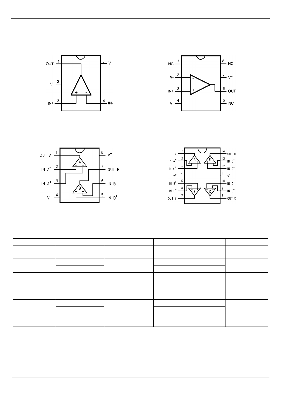
Connection Diagrams
LMP7707
5-Pin SOT23
20203702
Top View
LMP7707
8-Pin SOIC
20203701
Top View
LMP7708
8-Pin MSOP/SOIC
20203703
Top View
LMP7709
14-Pin TSSOP/SOIC
20203704
Top View
Ordering Information
Package Part Number Package Marking Transport Media NSC Drawing
5-Pin SOT23
LMP7707MF
AH4A
1k Units Tape and Reel
MF05A
LMP7707MFX 3k Units Tape and Reel
8-Pin SOIC
LMP7707MA
LMP7707MA
95 Units/Rail
M08A
LMP7707MAX 2.5k Units Tape and Reel
8-Pin MSOP
LMP7708MM
AJ4A
1k Units Tape and Reel
MUA08A
LMP7708MMX 3.5k Units Tape and Reel
8-Pin SOIC
LMP7708MA
LMP7708MA
95 Units/Rail
M08A
LMP7708MAX 2.5k Units Tape and Reel
14-Pin TSSOP
LMP7709MT
LMP7709MT
94 Units/Rail
MTC14
LMP7709MTX 2.5k Units Tape and Reel
14-Pin SOIC
LMP7709MA
LMP7709MA
55 Units/Rail
M14A
LMP7709MAX 2.5 Units Tape and Reel
7 www.national.com
LMP7707/LMP7708/LMP7709
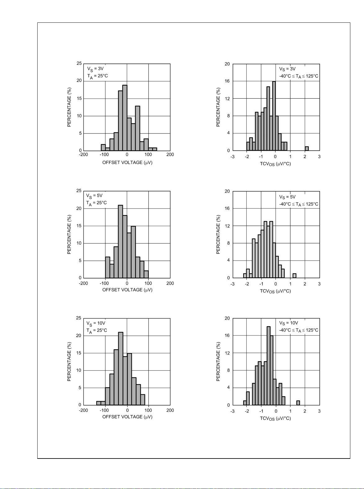
Typical Performance Characteristics Unless otherwise specified, T
A
= 25°C, V
CM
= V
S
/2, R
L
> 10 kΩ
connected to (V
+
+V
−
)/2
Offset Voltage Distribution
20203736
TCV
OS
Distribution
20203741
Offset Voltage Distribution
20203737
TCV
OS
Distribution
20203742
Offset Voltage Distribution
20203738
TCV
OS
Distribution
20203743
www.national.com 8
LMP7707/LMP7708/LMP7709
Loading...