


MM54HC157
MM54HC157/MM74HC157 Quad 2-Input Multiplexer
MM54HC158/MM74HC158 Quad 2-Input Multiplexer
(Inverted Output)
General Description
These high speed Quad 2-to-1 Line data selector/Multiplexers utilize advanced silicon-gate CMOS technology. They
possess the high noise immunity and low power consumption of standard CMOS integrated circuits, as well as the
ability to drive 10 LS-TTL loads.
These devices each consist of four 2-input digital multiplexers with common select and STROBE inputs. On the
MM54HC157/MM74HC157, when the STROBE input is at
logical ‘‘0’’ the four outputs assume the values as selected
from the inputs. When the STROBE input is at a logical ‘‘1’’
the outputs assume logical ‘‘0’’. The MM54HC158/
MM74HC158 operates in the same manner, except that its
outputs are inverted. Select decoding is done internally resulting in a single select input only. If enabled, the select
input determines whether the A or B inputs get routed to
their corresponding Y outputs.
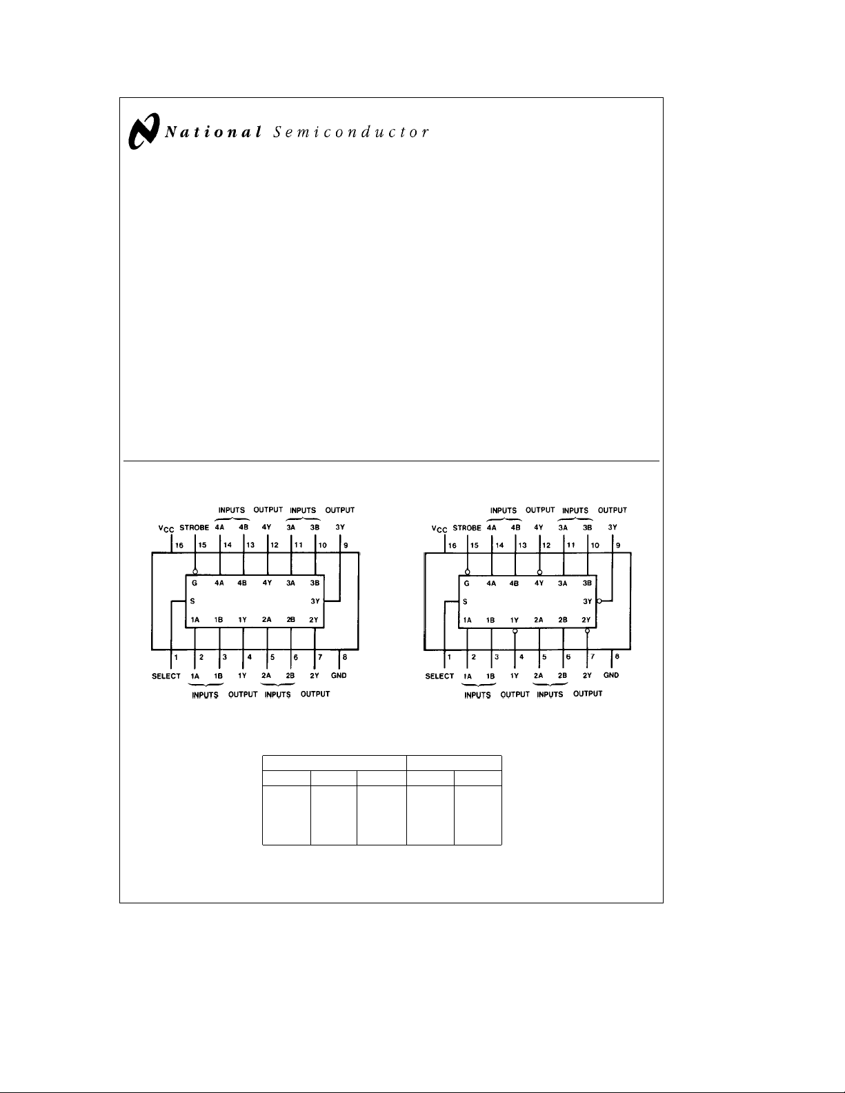
Connection Diagrams
Dual-In-Line Packages
The 54HC/74HC logic family is functionally as well as pinout compatible with the standard 54LS/74LS logic family.
All inputs are protected from damage due to static discharge by internal diode clamps to V
and ground.
CC
Features
Y
Typical propagation delay: 14 ns data to any output
Y
Wide power supply range: 2– 6V
Y
Low power supply quiescent current: 80 mA maximum
(74HC Series)
Y
Fan-out of 10 LS-TTL loads
Y
Low input current: 1 mA maximum
November 1995
MM54HC157/MM74HC157 Quad 2-Input Multiplexer
MM54HC158/MM74HC158 Quad 2-Input Multiplexer (Inverted Output)
Top View TL/F/5314– 1 Top View TL/F/5314– 2
Order Number MM54HC157/158 or MM74HC157/158
Function Table
Inputs Output Y
Strobe Select A B HC157 HC158
HXXXLH
LLLXLH
LLHXHL
LHXLLH
LHXHHL
e
H
High Level, LeLow Level, XeIrrelevant
C
1995 National Semiconductor Corporation RRD-B30M115/Printed in U. S. A.
TL/F/5314

Absolute Maximum Ratings (Notes1&2)
Operating Conditions
If Military/Aerospace specified devices are required,
please contact the National Semiconductor Sales
Office/Distributors for availability and specifications.
Supply Voltage (V
CC
)
DC Input Voltage (VIN)
DC Output Voltage (V
OUT
)
Clamp Diode Current (IIK,IOK)
DC Output Current, per pin (I
OUT
)
DC VCCor GND Current, per pin (ICC)
Storage Temperature Range (T
STG
b
b
)
b
0.5 toa7.0V
1.5 to V
0.5 to V
b
a
CC
a
CC
g
g
g
65§Ctoa150§C
1.5V
0.5V
20 mA
25 mA
50 mA
Supply Voltage (V
)26V
CC
DC Input or Output Voltage 0 V
(V
IN,VOUT
)
Operating Temp. Range (TA)
MM74HC
MM54HC
Input Rise or Fall Times
e
V
2.0V(tr,tf) 1000 ns
CC
e
V
4.5V 500 ns
CC
e
V
6.0V 400 ns
CC
Power Dissipation (PD)
(Note 3) 600 mW
S.O. Package only 500 mW
Lead Temp. (T
) (Soldering 10 seconds) 260§C
L
DC Electrical Characteristics (Note 4)
Symbol Parameter Conditions V
CC
A
e
T
25§C
Typ Guaranteed Limits
V
IH
Minimum High Level 2.0V 1.5 1.5 1.5 V
Input Voltage 4.5V 3.15 3.15 3.15 V
6.0V 4.2 4.2 4.2 V
V
IL
Maximum Low Level 2.0V 0.5 0.5 0.5 V
Input Voltage** 4.5V 1.35 1.35 1.35 V
6.0V 1.8 1.8 1.8 V
V
OH
Minimum High Level V
Output Voltage
e
VIHor V
l
I
IN
OUT
IL
s
20 mA 2.0V 2.0 1.9 1.9 1.9 V
l
4.5V 4.5 4.4 4.4 4.4 V
6.0V 6.0 5.9 5.9 5.9 V
e
V
VIHor V
IN
I
l
OUT
I
l
OUT
l
I
IN
OUT
e
V
OL
Maximum Low Level V
Output Voltage
IL
s
4.0 mA 4.5V 4.2 3.98 3.84 3.7 V
l
s
5.2 mA 6.0V 5.7 5.48 5.34 5.2 V
l
VIHor V
IL
s
20 mA 2.0V 0 0.1 0.1 0.1 V
l
4.5V 0 0.1 0.1 0.1 V
6.0V 0 0.1 0.1 0.1 V
e
V
VIHor V
IN
I
l
OUT
I
l
OUT
I
IN
I
CC
Note 1: Absolute Maximum Ratings are those values beyond which damage to the device may occur.
Note 2: Unless otherwise specified all voltages are referenced to ground.
Note 3: Power Dissipation temperature derating Ð plastic ‘‘N’’ package:
Note 4: For a power supply of 5V
designing with this supply. Worst case V
I
**V
Maximum Input V
Current
Maximum Quiescent V
Supply Current I
, and IOZ) occur for CMOS at the higher voltage and so the 6.0V values should be used.
CC
limits are currently tested at 20% of VCC. The above VILspecification (30% of VCC) will be implemented no later than Q1, CY’89.
IL
e
IN
e
IN
OUT
g
10% the worst case output voltages (VOH, and VOL) occur for HC at 4.5V. Thus the 4.5V values should be used when
and VILoccur at V
IH
IL
s
4.0 mA 4.5V 0.2 0.26 0.33 0.4 V
l
s
5.2 mA 6.0V 0.2 0.26 0.33 0.4 V
l
VCCor GND 6.0V
g
0.1
VCCor GND 6.0V 8.0 80 160 mA
e
0 mA
b
12 mW/§C from 65§Cto85§C; ceramic ‘‘J’’ package:b12 mW/§C from 100§Cto125§C.
e
5.5V and 4.5V respectively. (The VIHvalue at 5.5V is 3.85V.) The worst case leakage current (IIN,
CC
74HC 54HC
eb
T
40 to 85§CT
A
g
1.0
Min Max Units
V
§
§
Units
b
b
40
55
eb
A
55 to 125§C
g
CC
a
85
a
125
1.0 mA
C
C
2
 Loading...