

Motorola MC10E180FN, MC100E180FN Datasheet
SEMICONDUCTOR
TECHNICAL DATA
TV AND VCR
PLL TUNING CIRCUIT
WITH 1.3 GHz PRESCALER
AND I2C BUS
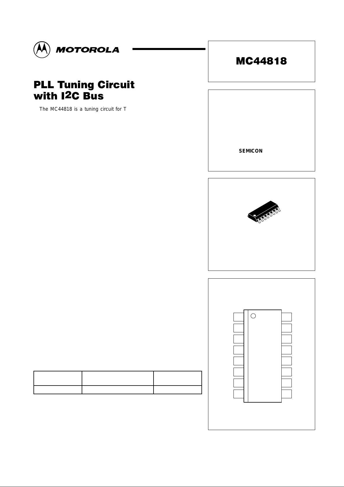
PIN CONNECTIONS
Order this document by MC44818/D
116
15
14
13
12
11
10
9
2
3
4
5
6
7
8
SDA
SCL
XTAL
V
CC2
33 V
V
CC1
5.0 V
HF In
AS
Gnd
D SUFFIX
PLASTIC PACKAGE
CASE 751B
(SO–16)
16
1
Amp In
V
TUN
Lock
V
CC3
12 V
B
3
B
2
B
1
B
0
(Top View)
1
MOTOROLA ANALOG IC DEVICE DATA
The MC44818 is a tuning circuit for TV and VCR tuner applications. It
contains, on one chip, all the functions required for PLL control of a VCO.
This integrated circuit also contains a high frequency prescaler and thus can
handle frequencies up to 1.3 GHz. The MC44818 is a pin compatible drop in
replacement for the MC44817, where the only difference is the MC44818
has a fixed divide–by–8 prescaler (cannot be bypassed) and the MC44817
uses the three wire bus.
The MC44818 has a programmable 512/1024 reference divider and is
manufactured on a single silicon chip using Motorola’s high density bipolar
process, MOSAIC (Motorola Oxide Self Aligned Implanted Circuits).
• Complete Single Chip System for MPU Control (I
2
C Bus). Data and
Clock Inputs are 3–Wire Bus Compatible
• Divide–by–8 Prescaler Accepts Frequencies up to 1.3 GHz
• 15 Bit Programmable Divider Accepts Input Frequencies up to 165 MHz
• Reference Divider: Programmable for Division Ratios 512 and 1024.
• 3–State Phase/Frequency Comparator
• Operational Amplifier for Direct Tuning Voltage Output (30 V)
• Four Integrated PNP Band Buffers for 40 mA (V
CC1
to 14.4 V)
• Output Options for the Reference Frequency and the
Programmable Divider
• High Sensitivity Preamplifier
• Circuit to Detect Phase Lock
• Fully ESD Protected
MOSAIC is a trademark of Motorola, Inc.
ORDERING INFORMATION
Device
Operating
Temperature Range
Package
MC44818D TA = –20° to +80°C SO–16
Motorola, Inc. 1996 Rev 2
MC44818
2
MOTOROLA ANALOG IC DEVICE DATA
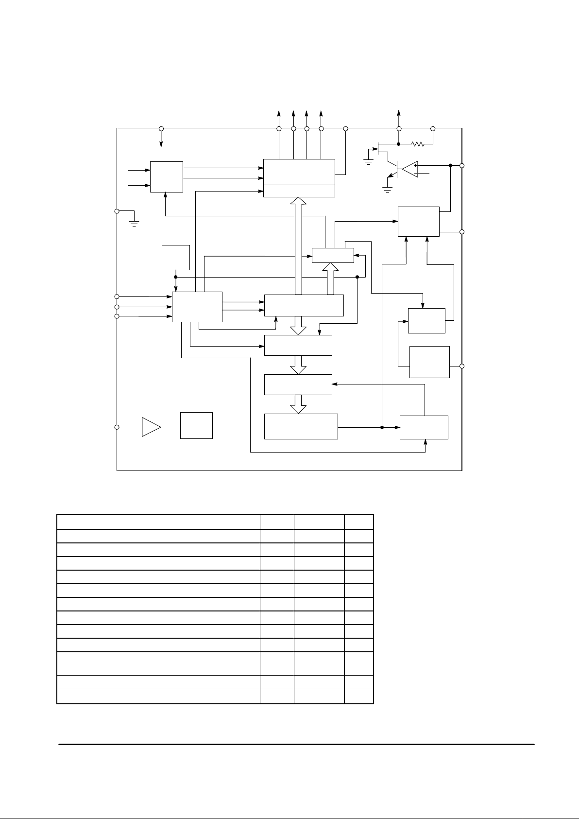
Representative Block Diagram
This device contains 3,204 active transistors.
Gnd
Test
Logic
Buffers
Latches
P–On
Reset
I2C Bus
Receiver
Latches
Phase
Comp
Ref
Divider
Osc
Latch Control
Program Divider
15 Bit
Latches B
Latches A
Shift Register
15 Bit
÷
8
Prescaler
DTB2
POR
Operational
Amplifier
2.7 V
20 k
DTB1
CL
Data
RL
DTF
F
out
TDI
F
out
F
ref
T10, T
11
T9, T12, T
14
T
13
4
6
15
10111213 14 5 675.0 V
F
out
F
ref
9
16
1
2
8
AS
Data
Clock
HF Input
V
CC1
V
CC3
V
TUN
V
CC2
Bands Out 30 mA
(40 mA at 0
°
to 80°C)
Amp In
Lock
XTAL
B3B2B1B
0
DTS, EN
512/1024
4
15
3
12 V
MAXIMUM RATINGS (T
A
= 25°C, unless otherwise noted.)
Rating Pin Value Unit
Power Supply Voltage (V
CC1
) 7 6.0 V
Band Buffer “Off” Voltage 10–13 14.4 V
Band Buffer “On” Current 10–13 50 mA
Band Buffer – Short Circuit Duration (0 to V
CC3
) (Note 2) 10–13 Continuous –
Operational Amplifier Power Supply Voltage (V
CC2
) 6 40 V
Operational Amplifier Short Circuit Duration (0 to V
CC2
) 5 Continuous –
Power Supply Voltage (V
CC3
) 14 14.4 V
Storage Temperature – –65 to +150 °C
Operating Temperature Range – –20 to +80 °C
Band Buffer Operation (Note 1) at 50 mA each Buffer All
Buffers “On” Simultaneously
10–13 10 sec
Operational Amplifier Output Voltage 5 V
CC2
V
RF Input Level (10 MHz to 1.3 GHz) – 1.5 Vrms
NOTES: 1. At V
CC3
= V
CC1
to 14.4 V and TA = –20° to +80°C.
2.At V
CC3
= V
CC1
to 14.4 V and TA = –20° to +80°C one buffer “On” only .
MC44818
3
MOTOROLA ANALOG IC DEVICE DATA
ELECTRICAL CHARACTERISTICS (V
CC1
= 5.0 V , V
CC2
= 33 V, V
CC3
= 12 V, TA = 25°C, unless otherwise noted.)
Characteristic
Pin Min Typ Max Unit
V
CC1
Supply Voltage Range 7 4.5 5.0 5.5 V
V
CC1
Supply Current (V
CC1
= 5.0 V) 7 – 37 50 mA
V
CC2
Supply Voltage Range 6 25 – 37 V
V
CC2
Supply Current (Output Open) 6 – 1.5 2.3 mA
Band Buffer Leakage Current when “Off” at 12 V 10–13 – 0.01 1.0 µA
Band Buffer Saturation Voltage when “On” at 30 mA 10–13 – 0.15 0.3 V
Band Buffer Saturation Voltage when “On” at 40 mA
only for 0° to 80°C
10–13 – 0.2 0.5 V
Data/Clock Current at 0 V 1, 2 –10 – 0 µA
Clock Current at 5.0 V 2 0 – 1.0 µA
Data Current at 5.0 V Acknowledge “Off” 1 0 – 1.0 µA
Data Saturation Voltage at 15 mA Acknowledge “On” 1 – – 1.0 V
Data/Clock Input Voltage Low 1, 2 – – 1.5 V
Data/Clock Input Voltage High 1, 2 3.0 – – V
Clock Frequency Range 2 – – 100 kHz
Oscillator Frequency Range 3 3.15 3.2 4.05 MHz
Operational Amplifier Internal Reference Voltage – 2.0 2.75 3.2 V
Operational Amplifier Input Current 4 –15 0 15 nA
DC Open Loop Voltage Gain – 100 250 – V/V
Gain Bandwidth Product (CL = 1.0 nF) – 0.3 – – MHz
V
out
Low, Sinking 50 µA 5 – 0.2 0.4 V
V
out
High, Sourcing 10 µA, V
CC2
– V
out
5 – 0.2 0.5 V
Phase Detector Current in the High Impedance State 4 –15 0 15 nA
Charge Pump High Current of Phase Comparator 4 30 50 85 µA
Charge Pump Low Current of Phase Comparator 4 10 15 30 µA
V
CC3
Supply Voltage Range 14 V
CC1
– 14.4 V
V
CC3
Supply Current 14 mA
All Buffers “Off” – 0.2 0.5
One Buffer “On” when Open – 8.0 13
One Buffer “On” at 40 mA – 48 53
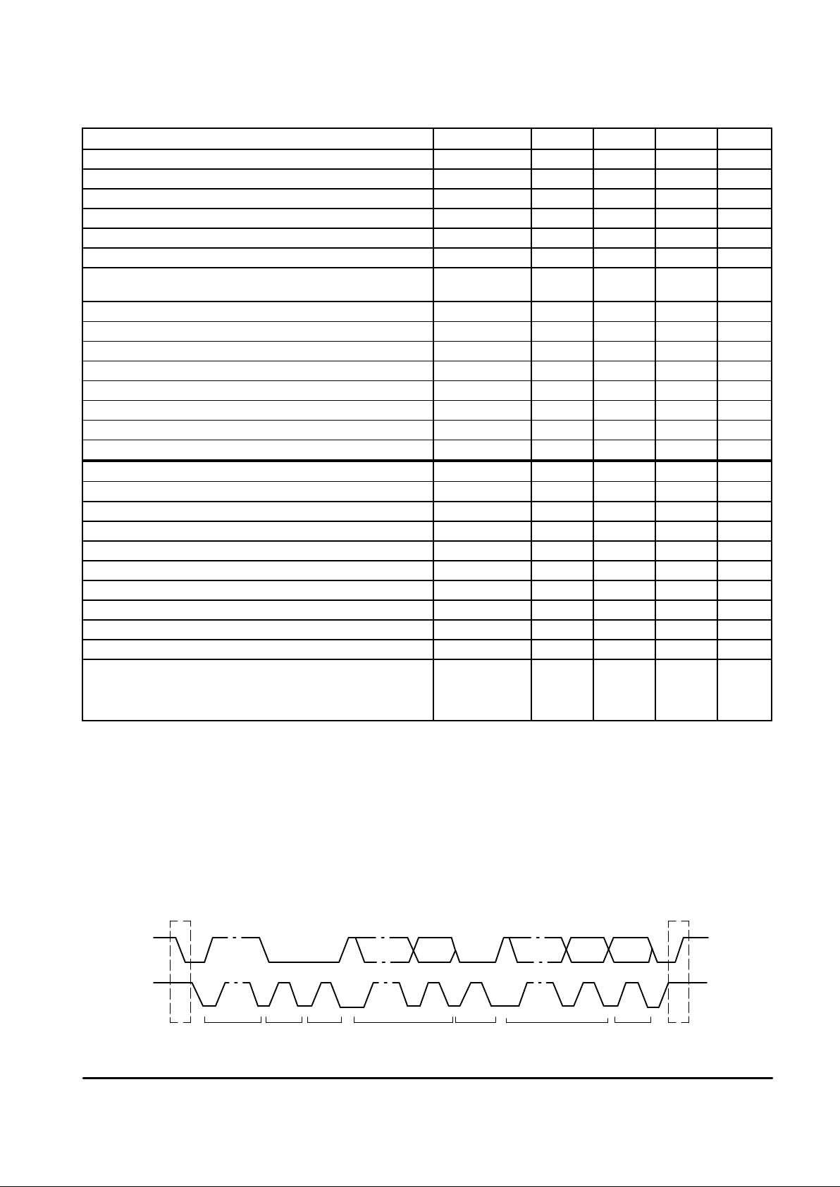
Data Format and Bus Receiver
The circuit receives the information for tuning and control
via the I2C bus. The incoming information, consisting of a
chip address byte followed by two or four data bytes, is
treated in the I2C bus receiver. The definition of the
permissible bus protocol is shown below:
1_ST A CA CO BA STO
2_ST A CA FM FL STO
3_ST A CA CO BA FM FL STO
4_ST A CA FM FL CO BA STO
STA = Start Condition
STO = Stop Condition
CA = Chip Address Byte
CO = Data Byte for Control Information
BA = Band Information
FM = Data Byte for Frequency Information
FL = Data Byte for Frequency Information
Figure 1. Complete Data Transfer Process
SDA
SCL
S P
1–7 8 9 1–7 8 9 1–7 8 9
STA ADDRESSCAR/W ACK DATA ACK DATA ACK STO
 Loading...