


 Loading...
Mitsubishi M37540M4-XXXGP, M37540M4-XXXFP, M37540E8GP, M37540E8FP, M37540RSS Datasheet
...
|
|
|
Y |
|
PRELIMINARThis |
|
|||
|
|
|
. . |
|
|
|
|
specification |
change |
|
|
|
to |
|
|
|
a |
final subject |
|
|
|
are |
|
|
is |
not |
|
||
|
limits |
|
||
|
|
|
|
|
Notice:parametric |
|
|
|
|
e |
|
|
|
|
Som |
|
|
|
|
MITSUBISHI MICROCOMPUTERS
7540 Group
SINGLE-CHIP 8-BIT CMOS MICROCOMPUTER
DESCRIPTION
The 7540 Group is the 8-bit microcomputer based on the 740 family core technology.
The 7540 Group has a serial I/O, 8-bit timers, a 16-bit timer, and an A-D converter, and is useful for control of home electric appliances and office automation equipment.
FEATURES
• |
Basic machine-language instructions ...................................... |
71 |
|
• |
The minimum instruction execution time |
......................... 0.34 s |
|
|
(at 6 MHz oscillation frequency, double-speed mode for the |
||
|
shortest instruction) |
|
|
• |
Memory size ROM .......................................... |
|
16 K to 32 K bytes |
|
RAM ............................................. |
|
512 to 768 bytes |
• |
Programmable I/O ports |
....................... |
29 (25 in 32-pin version) |
• |
Interrupts ................................................. |
|
15 sources, 15 vectors |
|
................................. (14 sources, 14 vectors for 32-pin version) |
||
• |
Timers ............................................................................. |
|
8-bit 4 |
|
...................................................................................... |
|
16-bit 1 |
• |
Serial I/O1 ................... |
8-bit 1 (UART or Clock-synchronized) |
|
• |
Serial I/O2 ................................... |
8-bit 1 (Clock-synchronized) |
|
• |
A-D converter ............................................... |
|
10-bit 8 channels |
|
.................................................... |
(6 channels for 32-pin version) |
|
• |
Clock generating circuit ............................................. |
|
Built-in type |
|
(low-power dissipation by a ring oscillator enabled) |
||
|
(connect to external ceramic resonator or quartz-crystal oscilla- |
||
|
tor permitting RC oscillation) |
|
|
• |
Watchdog timer ............................................................ |
16-bit 1 |
• |
Power source voltage |
|
|
XIN oscillation frequency at ceramic oscillation, in double-speed mode |
|
|
At 6 MHz .................................................................... |
4.5 to 5.5 V |
|
XIN oscillation frequency at ceramic oscillation, in high-speed mode |
|
|
At 8 MHz .................................................................... |
4.0 to 5.5 V |
|
At 4 MHz .................................................................... |
2.4 to 5.5 V |
|
At 2 MHz .................................................................... |
2.2 to 5.5 V |
|
XIN oscillation frequency at RC oscillation |
|
|
At 4 MHz .................................................................... |
4.0 to 5.5 V |
|
At 2 MHz .................................................................... |
2.4 to 5.5 V |
|
At 1 MHz .................................................................... |
2.2 to 5.5 V |
• |
Power dissipation |
|
|
Mask ROM version ....................................... |
22.5 mW (standard) |
|
One Time PROM version ................................ |
30 mW (standard) |
• |
Operating temperature range ................................... |
–20 to 85 °C |
(–40 to 85 °C for extended operating temperature version)
APPLICATION
Office automation equipment, factory automation equipment, home electric appliances, consumer electronics, car, etc.
Note: Serial I/O2 can be used in the following cases;
(1)Serial I/O1 is not used,
(2)Serial I/O1 is used as UART and BRG output divided by 16 is selected as the synchronized clock.
PIN CONFIGURATION (TOP VIEW)
|
|
|
|
|
|
|
P06 |
P05 |
P04 |
P03/TXOUT |
P02/TZOUT |
|
P01/TYOUT |
P00/CNTR1 |
P37/INT0 |
|
|
|
|
|
|
||||||||||
|
|
|
|
|
|
|
|
|
|
|
|
|
|
|
|
|
|
|
|
|
|
|
|
|
|
|
|
|
|
||
|
|
|
|
|
|
|
|
|
|
|
|
|
|
|
|
|
|
|
|
|
|
|
|
|
|
|
|
|
|
|
|
|
|
|
|
|
|
|
|
|
|
|
|
|
|
|
|
|
|
|
|
|
|
|
|
|
|
|
|
|
|
|
|
|
|
|
|
|
|
|
24 |
23 |
22 |
21 |
20 |
|
19 |
18 |
17 |
|
|
|
|
|
|
|
|||||||||
|
|
P07 |
|
|
|
|
|
|
|
|
|
|
|
|
|
|
|
|
|
|
|
|
|
|
|
|
|
|
|
P34(LED4) |
|
|
|
|
|
|
|
|
|
|
|
|
|
|
|
|
|
|
|
|
|
|
|
|
|
|
|
|
|
|
|||
25 |
|
|
|
|
|
|
|
|
|
|
|
|
|
|
|
|
|
|
|
16 |
|
|
|
|
|||||||
|
|
|
|
|
|
|
|
|
|
|
|
|
|
|
|
|
|
|
|
|
|||||||||||
|
P10/RXD1 |
|
|
|
|
|
|
|
|
|
|
|
|
|
|
|
|
|
|
|
|
|
|
|
|
|
|
|
P33(LED3) |
||
26 |
|
|
|
|
|
|
|
|
|
|
|
|
|
|
|
|
|
|
|
15 |
|
|
|
|
|||||||
|
|
|
|
|
|
|
|
|
|
|
|
|
|
|
|
|
|
|
|
|
|||||||||||
|
|
|
|
|
|
|
|
|
|
|
|
|
|
|
|
|
|
|
|
|
|||||||||||
|
P11/TXD1 |
|
|
27 |
M37540M4-XXXGP |
14 |
|
|
|
|
P32(LED2) |
||||||||||||||||||||
|
|
||||||||||||||||||||||||||||||
|
|
||||||||||||||||||||||||||||||
P12/SCLK1/SCLK2 |
|
|
28 |
13 |
|
|
|
|
P31(LED1) |
||||||||||||||||||||||
|
|
||||||||||||||||||||||||||||||
|
|
|
|
|
|
M37540M4T-XXXGP |
|
|
|
|
|
|
|||||||||||||||||||
P13/SRDY1 |
/SDATA2 |
|
|
|
|
|
|
|
|
P30(LED0) |
|||||||||||||||||||||
|
|
29 |
12 |
|
|
|
|
||||||||||||||||||||||||
|
P14/CNTR0 |
|
|
|
|
|
|
M37540E8GP |
|
|
|
|
|
|
|
|
VSS |
||||||||||||||
30 |
|
|
|
|
|
|
11 |
|
|
|
|
||||||||||||||||||||
|
|
|
|
|
|
|
|||||||||||||||||||||||||
|
|
|
|
|
|
|
|
||||||||||||||||||||||||
|
P20/AN0 |
|
|
31 |
|
|
|
|
|
|
|
|
|
|
|
|
|
|
|
|
|
|
|
10 |
|
|
|
|
XOUT |
||
|
|
|
|
|
|
|
|
|
|
|
|
|
|
|
|
|
|
|
|
|
|
|
|
|
|||||||
|
P21/AN1 |
|
|
|
|
|
|
|
|
|
|
|
|
|
|
|
|
|
|
|
|
|
|
|
|
|
|
|
XIN |
||
|
|
32 |
|
|
|
|
|
|
|
|
|
|
|
|
|
|
|
|
|
|
|
9 |
|
|
|
|
|||||
|
|
|
|
|
|
|
|
|
|
|
|
|
|
|
|
|
|
|
|
|
|
|
|
|
|
|
|
|
|
|
|
|
|
|
|
|
|
|
1 |
2 |
3 |
4 |
5 |
|
6 |
7 |
8 |
|
|
|
|
|
|
|
|||||||||
|
|
|
|
|
|
|
|
|
|
|
|
|
|
|
|
|
|
|
|
|
|
|
|
|
|
|
|
|
|
|
|
|
|
|
|
|
|
|
|
|
|
|
|
|
|
|
|
|
|
|
|
|
VCC |
|
|
|
|
|
|
||||
|
|
|
|
|
|
|
|
|
|
|
|
|
|
|
|
|
|
|
|
|
|
|
|
|
|
|
|
||||
|
|
|
|
|
|
|
|
|
|
|
|
|
|
|
|
|
|
|
|
|
|
|
|
|
|||||||
|
|
|
|
|
|
|
P22/AN2 |
P23/AN3 |
P24/AN4 |
P25/AN5 |
VREF |
|
RESET |
CNVSS |
|
|
|
|
|
|
|||||||||||
|
|
|
|
|
|
|
|
|
|
|
|
|
|
||||||||||||||||||
|
|
|
|
|
|
|
|
|
|
|
|
|
|
|
|
|
|
|
|
|
|
|
|||||||||
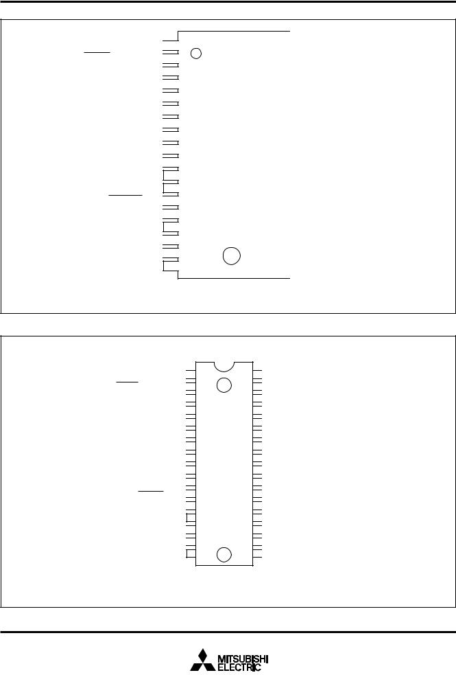
Package type: 32P6U-A
Fig. 1 M37540M4-XXXGP, M37540E8GP, M37540M4T-XXXGP pin configuration
|
|
|
Y |
|
PRELIMINARThis |
|
|||
|
|
|
. . |
|
|
|
|
specification |
change |
|
|
|
to |
|
|
|
a |
final subject |
|
|
not |
are |
|
|
is |
|
|
||
|
limits |
|
||
|
|
|
|
|
Notice:parametric |
|
|
|
|
Some |
|
|
|
|
MITSUBISHI MICROCOMPUTERS
7540 Group
SINGLE-CHIP 8-BIT CMOS MICROCOMPUTER
P12/SCLK1/SCLK2 

 1
1
P13/SRDY1/SDATA2 

 2
2
P14/CNTR0 

 3
3
P20/AN0 

 4
4
P21/AN1 

 5
5
P22/AN2 

 6
6
P23/AN3 

 7
7
P24/AN4 

 8
8
P25/AN5 

 9
9
P26/AN6 

 10
10
P27/AN7 
 11
11
VREF  12
12
RESET 
 13
13
CNVSS 
 14
14
Vcc 15
XIN 
 16
16
XOUT 
 17
17
VSS 18
XXXFP-M37540M4 XXXFP-M37540M4T M37540E8FP
|
|
|
|
|
|
P11/TXD1 |
36 |
|
|
|
|
|
|
|
|
|
|
|
|
P10/RXD1 |
35 |
|
|
|
|
|
|
|
|
|
|
|
|
P07 |
34 |
|
|
|
|
|
|
|
|
|
|
|
|
P06 |
33 |
|
|
|
|
|
|
|
|
|
|
|
|
P05 |
32 |
|
|
|
|
|
|
|
|
|
|
|
|
P04 |
31 |
|
|
|
|
|
|
|
|
|
|
|
|
P03/TXOUT |
30 |
|
|
|
|
|
|
|
|
|
|
|
|
P02/TZOUT |
29 |
|
|
|
|
|
|
|
|
|
|
|
|
P01/TYOUT |
28 |
|
|
|
|
|
|
|
|
|
|
|
|
P00/CNTR1 |
27 |
|
|
|
|
|
|
|
|
|
|
|
|
P37/INT0 |
26 |
|
|
|
|
|
|
|
|
|
|
|
||
|
|
|
|
|
|
P36(LED6)/INT1 |
25 |
|
|
|
|
|
|
|
|
|
|
|
|
P35(LED5) |
24 |
|
|
|
|
|
|
|
|
|
|
|
||
|
|
|
|
|
|
P34(LED4) |
23 |
|
|
|
|
|
|
|
|
|
|
|
|
P33(LED3) |
22 |
|
|
|
|
|
|
|
|
|
|
|
|
P32(LED2) |
21 |
|
|
|
|
|
|
|
|
|
|
|
|
|
20 |
|
|
|
|
|
P31(LED1) |
|
|
|
|
|
||
|
|
|
|
|
|
|
19 |
|
|
|
|
|
P30(LED0) |
|
|
|
|
|
|
|
Package type: 36P2R-A
Fig. 2 M37540M4-XXXFP, M37540M4T-XXXFP, M37540E8FP pin configuration
P12/SCLK1/SCLK2 

 1
1
P13/SRDY1/SDATA2
 2
2
P14/CNTR0 

 3
3
P20/AN0 

 4
4
P21/AN1 

 5
5
P22/AN2 

 6
6
P23/AN3 

 7
7
P24/AN4 

 8
8
P25/AN5 

 9
9
VREF 
 10
10
RESET 
 11
11
CNVSS 
 12
12
VCC 13
XIN 
 14
14
XOUT
 15
15
VSS 16
XXXSP-M37540M4 M37540E8SP
32

 P11/TXD1 31

 P10/RXD1 30

 P07
P07
29

 P06
P06
28

 P05
P05
27

 P04
P04
26

 P03/TXOUT
25

 P02/TZOUT
24

 P01/TYOUT
23

 P00/CNTR1
22

 P37/INT0 21

 P34(LED4)
20

 P33(LED3)
19 

 P32(LED2)
18 

 P31(LED1)
17 

 P30(LED0)
Package type: 32P4B
Fig. 3 M37540M4-XXXSP, M37540E8SP pin configuration
2

|
|
|
Y |
|
PRELIMINARThis |
|
|||
|
|
|
. . |
|
|
|
|
specification |
change |
|
|
|
to |
|
|
|
a |
final subject |
|
|
not |
are |
|
|
is |
|
|
||
|
limits |
|
||
|
|
|
|
|
Notice:parametric |
|
|
|
|
e |
|
|
|
|
Som |
|
|
|
|
MITSUBISHI MICROCOMPUTERS
7540 Group
SINGLE-CHIP 8-BIT CMOS MICROCOMPUTER
P14/CNTR0 |
|
|
|
|
|
|
|
|
|
|
|
|
|
|
|
|
||
|
|
|
|
|
|
|
|
1 |
|
|||||||||
|
NC |
|
|
|||||||||||||||
2 |
|
|||||||||||||||||
|
NC |
|
|
|||||||||||||||
3 |
|
|||||||||||||||||
P20/AN0 |
|
|
|
|
|
|
|
|
|
|
|
|||||||
|
|
|
|
|
|
|
|
|
4 |
|
||||||||
P21/AN1 |
|
|
|
|
|
|
|
|
|
|
|
|||||||
|
|
|
|
|
|
|
|
|
5 |
|
||||||||
|
NC |
|
|
|||||||||||||||
6 |
|
|||||||||||||||||
P22/AN2 |
|
|
|
|
|
|
|
|
|
|
|
|
||||||
|
|
|
|
|
|
|
|
|
|
7 |
M37540RSS |
|||||||
P23/AN3 |
|
|
|
|
|
|
|
|
|
|
|
|
|
|
|
|||
|
|
|
|
|
|
|
|
|
|
|
|
|
|
8 |
||||
|
|
|
|
|
|
|
|
|
|
|
||||||||
P24/AN4 |
|
|
|
|
|
|
|
|
|
|||||||||
9 |
|
|||||||||||||||||
|
|
|
|
|
|
|
|
|||||||||||
P25/AN5 |
|
|
|
|
|
|
|
|
|
|
|
|
|
|
||||
10 |
|
|||||||||||||||||
|
|
|
|
|
|
|
|
|
|
|
|
|
||||||
P26/AN6 |
|
|
|
|
|
|
|
|
|
|
||||||||
|
|
|
|
|
|
|
|
11 |
|
|||||||||
P27/AN7 |
|
|
|
|
|
|
||||||||||||
12 |
|
|||||||||||||||||
|
|
|
|
|
||||||||||||||
|
NC |
|
|
|||||||||||||||
13 |
|
|||||||||||||||||
|
NC |
|
|
|||||||||||||||
14 |
|
|||||||||||||||||
|
VREF |
|
|
|
|
|
||||||||||||
|
|
|
|
15 |
|
|||||||||||||
|
|
|
|
|
|
|
|
|
|
|
||||||||
|
RESET |
|
|
|
|
|
|
|
|
|||||||||
|
|
|
|
|
|
16 |
|
|||||||||||
|
CNVSS |
|
|
|
|
|
|
|
||||||||||
|
|
|
|
|
|
17 |
|
|||||||||||
|
Vcc |
|
|
|||||||||||||||
18 |
|
|||||||||||||||||
|
XIN |
|
|
|
|
|
|
|
||||||||||
|
|
|
|
|
19 |
|
||||||||||||
|
XOUT |
|
|
|
|
|
|
|
||||||||||
|
|
|
|
|
20 |
|
||||||||||||
|
VSS |
|
|
|||||||||||||||
21 |
|
|||||||||||||||||
|
|
|
|
|
|
|
|
|
|
|
|
|
|
|
|
|
|
|
Outline 42S1M
Fig. 4 M37540RSS pin configuration
|
|
|
|
|
|
|
|
|
|
42 |
|
|
|
|
|
|
P13/SRDY1/SDATA2 |
||
|
|
|
|
|
|
||||
41 |
|
|
|
|
|
|
P12/SCLK1/SCLK2 |
||
|
|
|
|
|
|
||||
|
|
|
|
|
|
||||
40 |
|
|
|
|
|
|
P11/TXD1 |
||
|
|||||||||
|
|
|
|
|
|
||||
39 |
|
|
|
|
|
|
P10/RXD1 |
||
|
|||||||||
|
|
|
|
|
|
||||
38 |
|
|
|
|
|
|
P07 |
||
|
|||||||||
|
|
|
|
|
|
||||
37 |
|
|
|
|
|
|
P06 |
||
|
|||||||||
|
|
|
|
|
|
||||
36 |
|
|
|
|
|
|
P05 |
||
|
|||||||||
|
|
|
|
|
|
||||
35 |
|
|
|
|
|
|
P04 |
||
|
|
|
|
|
|
||||
34 |
|
|
|
|
|
|
P03/TXOUT |
||
|
|
|
|
|
|
||||
33 |
|
|
|
|
|
|
P02/TZOUT |
||
|
|
|
|
|
|
||||
32 |
|
|
|
|
|
|
P01/TYOUT |
||
|
|||||||||
|
|
|
|
|
|
||||
31 |
|
|
|
|
|
|
P00/CNTR1 |
||
|
|||||||||
|
|
|
|
|
|
||||
30 |
|
|
|
|
|
|
NC |
||
|
|||||||||
29 |
|
|
|
|
|
|
P37/INT0 |
||
|
|||||||||
|
|
|
|
|
|
||||
28 |
|
|
|
|
|
|
P36(LED6)/INT1 |
||
|
|||||||||
|
|
|
|
|
|
||||
27 |
|
|
|
|
|
|
P35(LED5) |
||
|
|
|
|
|
|
||||
26 |
|
|
|
|
|
|
P34(LED4) |
||
|
|
|
|
|
|
||||
|
|
|
|
|
|
||||
25 |
|
|
|
|
|
|
P33(LED3) |
||
|
|
|
|
|
|
||||
|
|
|
|
|
|
||||
24 |
|
|
|
|
|
|
P32(LED2) |
||
|
|
|
|
|
|
||||
|
|
|
|
|
|
||||
23 |
|
|
|
|
|
|
P31(LED1) |
||
|
|
|
|
|
|
||||
|
|
|
|
|
|
||||
22 |
|
|
|
|
|
|
P30(LED0) |
||
|
|
|
|
|
|
||||
3
|
|
|
Y |
|
PRELIMINARThis |
|
|||
|
|
|
. . |
|
|
|
|
specification |
change |
|
|
|
to |
|
|
|
a |
final subject |
|
|
not |
are |
|
|
is |
|
|
||
|
limits |
|
||
|
|
|
|
|
Notice:parametric |
|
|
|
|
Some |
|
|
|
|
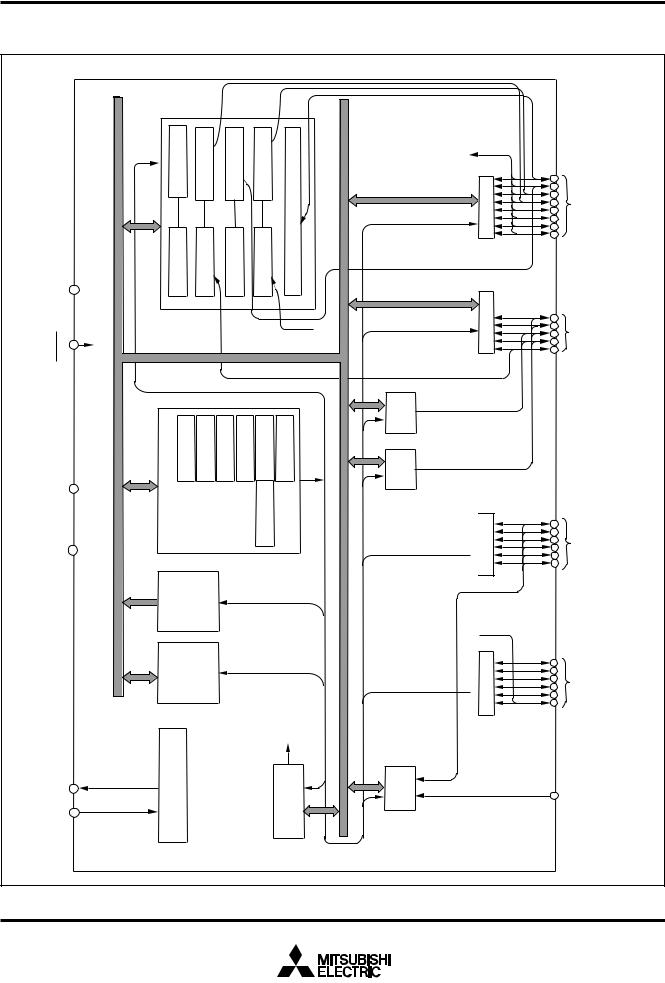
FUNCTIONAL BLOCK
MITSUBISHI MICROCOMPUTERS
7540 Group
SINGLE-CHIP 8-BIT CMOS MICROCOMPUTER
|
|
|
Timer1(8) |
TXOUT |
|
CNVSS |
7 |
Prescaler1(8) |
|
Resetinput |
RESET |
6 |
|
INT0 |
|
|
VCC |
8 |
32P6U) |
|
VSS |
11 |
DIAGRAM(Package: |
Clockinput Clockoutput |
|
|
FUNCTIONALBLOCK |
X |
9 |
|
|
|
OUT |
10 |
|
|
X |
|
|
|
IN |
|
Fig. 5 Functional block diagram (32P6U package)
Key-onwakeup
P0(8) |
24232221201918 |
I/OportP0 |
|
25 |
|
P1(5) |
3029282726 |
I/OportP1 |
SI/O1(8) SI/O2(8)

 P2(6)
P2(6)
INT0

 P3(6)
P3(6)
2 13231 |
portP2 |
4 3 |
I/O |
15141312 |
portP3 |
1716 |
I/O |
A-D converter (10) |
5 |
VREF |
4

|
|
|
Y |
|
PRELIMINARThis |
|
|||
|
|
|
. . |
|
|
|
|
specification |
change |
|
|
|
to |
|
|
|
a |
final subject |
|
|
not |
are |
|
|
is |
|
|
||
|
limits |
|
||
|
|
|
|
|
Notice:parametric |
|
|
|
|
e |
|
|
|
|
Som |
|
|
|
|
MITSUBISHI MICROCOMPUTERS
7540 Group
SINGLE-CHIP 8-BIT CMOS MICROCOMPUTER
|
|
|
|
Prescaler1(8) Timer1(8) |
|
(8) |
|
(8) |
TYOUT |
PrescalerZ(8) TimerZ(8) |
TZOUT |
|
|
|
|
|
Key-onwakeup |
|
|
|
|
|
|
|
|
TimerX |
TXCNTROUT0 |
TimerY |
|
|
|
|
|
|
|
|
|||||
|
|
|
|
|
TimerA(16) |
|
|
|
|
|
3433323130292827 |
|
I/OportP0 |
|||||||
|
|
CNVSS |
14 |
|
PrescalerX(8) |
PrescalerY(8) |
CNTR1 |
|
|
|
P0(8) |
|
||||||||
|
Resetinput |
RESET |
13 |
|
|
|
|
|
|
|
|
|
INT0 |
|
|
|
P1(5) |
3 2 1 3635 |
|
I/OportP1 |
|
|
|
|
|
|
|
|
|
|
|
|
|
|
|
SI/O2(8) |
|
|
|
|
|
|
|
VCC |
15 |
|
A |
X |
|
Y |
S |
PCL |
|
PS |
|
|
SI/O1(8) |
|
|
|
|
|
36P2R) |
|
VSS |
18 |
|
ROM |
|
|
|
|
PCH |
|
|
|
|
|
|
P2(8) |
1110 9 8 7 6 5 4 |
|
I/OportP2 |
(Package: |
|
|
|
|
|
|
|
|
|
|
|
|
|
|
|
INTINT01 |
19 |
|
|
|
FUNCTIONALBLOCKDIAGRAM |
Clockinput Clockoutput |
OUT |
16 17 |
Clockgeneratingcircuit |
RAM |
|
|
|
|
|
|
WatchdogtimerReset |
|
A-D |
converter |
(10) |
P3(8) |
12 26252423222120 |
VREF |
I/OportP3 |
X |
|
|
|
|
|
|
|
|||||||||||||
IN |
|
|
|
|
|
|
|
|||||||||||||
X |
|
|
|
|
|
|
|
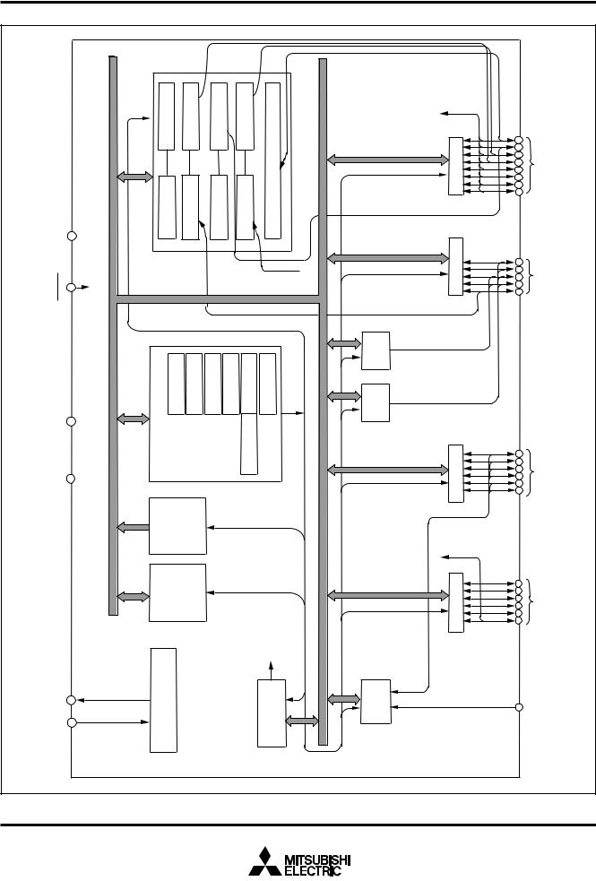
Fig. 6 Functional block diagram (36P2R package)
5
|
|
|
Y |
|
PRELIMINARThis |
|
|||
|
|
|
. . |
|
|
|
|
specification |
change |
|
|
|
to |
|
|
|
a |
final subject |
|
|
not |
are |
|
|
is |
|
|
||
|
limits |
|
||
|
|
|
|
|
Notice:parametric |
|
|
|
|
Some |
|
|
|
|
MITSUBISHI MICROCOMPUTERS
7540 Group
SINGLE-CHIP 8-BIT CMOS MICROCOMPUTER
|
|
|
|
(8) |
|
(8) |
|
(8) |
TYOUT |
(8) |
TZOUT |
|
|
|
|
|
Key-onwakeup |
|
|
|
|
|
|
|
|
Timer1 |
|
PrescalerX(8) TimerX |
TXCNTROUT0 |
PrescalerY(8) TimerY |
PrescalerZ(8) TimerZ |
|
|
|
|
|
|
|
|
||||
|
|
|
|
|
TimerA(16) |
|
|
|
|
|
|
3029282726252423 |
|
I/OportP0 |
|||||||
|
|
CNVSS |
12 |
Prescaler1(8) |
|
CNTR1 |
|
|
|
|
P0(8) |
|
|||||||||
|
Resetinput |
RESET |
11 |
|
|
|
|
|
|
|
|
|
INT0 |
|
|
|
|
P1(5) |
3 2 13231 |
|
I/OportP1 |
|
|
|
|
|
|
|
|
|
|
|
|
|
|
|
SI/O2(8) |
|
|
|
|
|
|
|
|
VCC |
13 |
CPU |
A |
X |
Y |
|
S |
PCL |
|
PS |
|
|
SI/O1(8) |
|
|
|
|
|
|
32P4B) |
|
VSS |
16 |
|
ROM |
|
|
|
|
PCH |
|
|
|
|
|
|
|
P2(6) |
9 8 7 6 5 4 |
|
I/OportP2 |
FUNCTIONALBLOCKDIAGRAM(Package: |
|
|
|
|
|
|
|
|
|
|
|
|
|
|
|
|
|
|
|
|
|
Clockinput Clockoutput |
OUT |
15 |
Clockgeneratingcircuit |
RAM |
|
|
|
|
|
|
ResetWatchdogtimer |
|
A-D |
converter |
(10) |
INT0 |
P3(6) |
10 222120191817 |
VREF |
I/OportP3 |
|
X |
|
|
|
|
|
|
|
|
|||||||||||||
IN |
14 |
|
|
|
|
|
|
|
|||||||||||||
X |
|
|
|
|
|
|
|
||||||||||||||
Fig. 7 Functional block diagram (32P4B package)
6

|
|
|
Y |
|
PRELIMINARThis |
|
|||
|
|
|
. . |
|
|
|
|
specification |
change |
|
|
|
to |
|
|
|
a |
final subject |
|
|
not |
are |
|
|
is |
|
|
||
|
limits |
|
||
|
|
|
|
|
Notice:parametric |
|
|
|
|
e |
|
|
|
|
Som |
|
|
|
|
MITSUBISHI MICROCOMPUTERS
7540 Group
SINGLE-CHIP 8-BIT CMOS MICROCOMPUTER
PIN DESCRIPTION
Table 1 Pin description
|
|
Pin |
Name |
Function |
|
||
|
|
Function expect a port function |
|||||
|
Vcc, Vss |
Power source |
•Apply voltage of 2.2 to 5.5 V to Vcc, and 0 V to Vss. |
|
|||
|
|
|
|
|
(Note 1) |
|
|
|
|
|
|
|
|
|
|
|
VREF |
Analog reference |
•Reference voltage input pin for A-D converter |
|
|||
|
|
|
|
|
voltage |
|
|
|
|
|
|
|
|
|
|
|
CNVss |
CNVss |
•Chip operating mode control pin, which is always connected to Vss. |
||||
|
|
|
|
|
|
|
|
|
|
|
|
|
Reset input |
•Reset input pin for active “L” |
|
|
RESET |
|
|||||
|
XIN |
Clock input |
•Input and output pins for main clock generating circuit |
|
|||
|
|
|
|
|
|
•Connect a ceramic resonator or quartz crystal oscillator between the XIN and XOUT pins. |
|
|
XOUT |
Clock output |
•For using RC oscillator, short between the XIN and XOUT pins, and connect the capacitor and resistor. |
||||
|
|
|
|
|
|
•If an external clock is used, connect the clock source to the XIN pin and leave the XOUT pin open. |
|
|
|
|
|
|
|
|
|
|
P00/CNTR1 |
I/O port P0 |
•8-bit I/O port. |
• Key-input (key-on wake up |
|||
|
P01/TYOUT |
|
•I/O direction register allows each pin to be individually pro- |
interrupt input) pins |
|||
|
P02/TZOUT |
|
• Timer Y, timer Z, timer X and |
||||
|
|
grammed as either input or output. |
|||||
|
P03/TXOUT |
|
|||||
|
|
•CMOS compatible input level |
timer A function pin |
||||
|
P04–P07 |
|
|||||
|
|
|
|||||
|
|
•CMOS 3-state output structure |
|
||||
|
|
|
|
|
|
|
|
|
|
|
|
|
|
•Whether a built-in pull-up resistor is to be used or not can be de- |
|
|
|
|
|
|
|
termined by program. |
|
|
|
|
|
|
|
|
|
|
P10/RxD1 |
I/O port P1 |
•5-bit I/O port |
• Serial I/O1 function pin |
|||
|
P11/TxD1 |
|
•I/O direction register allows each pin to be individually pro- |
|
|||
|
P12/SCLK1/SCLK2 |
|
• Serial I/O1 function pin |
||||
|
|
grammed as either input or output. |
|||||
|
|
|
/SDATA2 |
|
|
• Serial I/O2 function pin |
|
|
P13/SRDY1 |
|
•CMOS compatible input level |
||||
|
P14/CNTR0 |
|
•CMOS 3-state output structure |
• Timer X function pin |
|||
|
|
|
|
|
|
|
|
|
|
|
|
|
|
•CMOS/TTL level can be switched for P10, P12 and P13 |
|
|
|
|
|
|
|
||
P20/AN0–P27/AN7 |
I/O port P2 |
•8-bit I/O port having almost the same function as P0 |
• Input pins for A-D converter |
||||
|
|
|
|
|
(Note 2) |
•CMOS compatible input level |
|
|
|
|
|
|
|
•CMOS 3-state output structure |
|
P30–P35 |
I/O port P3 |
•8-bit I/O port |
|
||||
|
|
|
|
|
(Note 3) |
•I/O direction register allows each pin to be individually programmed as either input or output. |
|
|
|
|
|
|
|
•CMOS compatible input level (CMOS/TTL level can be switched for P36 and P37). |
|
|
|
|
|
|
|
•CMOS 3-state output structure |
|
|
|
|
|
|
|
•P30 to P36 can output a large current for driving LED. |
|
P36/INT1 |
|
•Whether a built-in pull-up resistor is to be used or not can be de- |
• Interrupt input pins |
||||
P37/INT0 |
|
termined by program. |
|
||||
|
|
|
|||||
Notes 1: VCC = 2.4 to 5.5 V for the extended operating temperature version.
2:P26/AN6 and P27/AN7 do not exist for the 32-pin version, so that Port P2 is a 6-bit I/O port.
3:P35 and P36/INT1 do not exist for the 32-pin version, so that Port P3 is a 6-bit I/O port.
7
|
|
|
Y |
|
PRELIMINARThis |
|
|||
|
|
|
. . |
|
|
|
|
specification |
change |
|
|
|
to |
|
|
|
a |
final subject |
|
|
not |
are |
|
|
is |
|
|
||
|
limits |
|
||
|
|
|
|
|
Notice:parametric |
|
|
|
|
Some |
|
|
|
|
MITSUBISHI MICROCOMPUTERS
7540 Group
SINGLE-CHIP 8-BIT CMOS MICROCOMPUTER
GROUP EXPANSION |
Memory size |
|
|
|
Mitsubishi plans to expand the 7540 group as follow: |
ROM/PROM size |
............................................... |
|
16 K to 32 K bytes |
|
RAM size .............................................................. |
|
|
512 to 768 bytes |
Memory type |
|
|
|
|
Support for Mask ROM version, One Time PROM version, and |
Package |
|
|
|
Emulator MCU. |
32P4B ......................................... |
|
32-pin shrink plastic molded DIP |
|
|
32P6U-A .................................. |
|
0.8 mm-pitch plastic molded LQFP |
|
|
36P2R-A ................................. |
|
0.8 mm-pitch plastic molded SSOP |
|
|
42S1M .................................... |
42 - pin shrink ceramic PIGGY BACK |
||
|
|
|
|
|
ROM size |
|
|
|
|
(bytes) |
|
Under development |
||
32K |
|
|
||
|
|
M37540E8 |
|
|
Under development
M37540M4T
16K |
M37540M4 |
Under development
0 |
384 |
512 |
768 RAM size |
|
|
|
(bytes) |
Note: Products under development•••the development schedule and specification may be revised without notice.
Fig. 8 Memory expansion plan
Currently supported products are listed below.
Table 2 List of supported products
Product |
(P) ROM size (bytes) |
RAM size |
Package |
|
|
Remarks |
|||
ROM size for User () |
(bytes) |
|
|
||||||
|
|
|
|
|
|
||||
M37540M4-XXXSP |
16384 |
|
512 |
32P4B |
Mask ROM version |
||||
M37540M4-XXXFP |
(16254) |
|
|
36P2R-A |
Mask ROM version |
||||
M37540M4T-XXXFP |
|
|
|
|
|
|
Mask ROM version (extended operating temperature version) |
||
M37540M4-XXXGP |
|
|
|
|
32P6U-A |
Mask ROM version |
|||
M37540M4T-XXXGP |
|
|
|
|
|
|
Mask ROM version (extended operating temperature version) |
||
|
|
|
|
|
|
|
|||
M37540E8SP |
32768 |
|
768 |
32P4B |
One Time PROM version (blank) |
||||
M37540E8FP |
(32638) |
|
|
36P2R-A |
One Time PROM version (blank) |
||||
M37540E8GP |
|
|
|
|
32P6U-A |
One Time PROM version (blank) |
|||
M37540RSS |
|
|
|
768 |
42S1M |
Emulator MCU |
|||
|
|
|
|||||||
|
|
|
|
|
|
|
|
|
|
|
|
|
|
|
|
|
|
|
|
|
|
|
|
|
|
|
|
|
|
|
|
|
|
|
|
|
|
|
|
8

|
|
|
Y |
|
PRELIMINARThis |
|
|||
|
|
|
. . |
|
|
|
|
specification |
change |
|
|
|
to |
|
|
|
a |
final subject |
|
|
not |
are |
|
|
is |
|
|
||
|
limits |
|
||
|
|
|
|
|
Notice:parametric |
|
|
|
|
e |
|
|
|
|
Som |
|
|
|
|
MITSUBISHI MICROCOMPUTERS
7540 Group
SINGLE-CHIP 8-BIT CMOS MICROCOMPUTER
FUNCTIONAL DESCRIPTION
Central Processing Unit (CPU)
The MCU uses the standard 740 family instruction set. Refer to the table of 740 family addressing modes and machine-language instructions or the SERIES 740 <SOFTWARE> USER’S MANUAL for details on each instruction set.
Machine-resident 740 family instructions are as follows:
1.The FST and SLW instructions cannot be used.
2.The MUL and DIV instructions can be used.
3.The WIT instruction can be used.
4.The STP instruction can be used.
This instruction cannot be used while CPU operates by a ring oscillator.
Accumulator (A)
The accumulator is an 8-bit register. Data operations such as data transfer, etc., are executed mainly through the accumulator.
Stack pointer (S)
The stack pointer is an 8-bit register used during subroutine calls and interrupts. The stack is used to store the current address data and processor status when branching to subroutines or interrupt routines.
The lower eight bits of the stack address are determined by the contents of the stack pointer. The upper eight bits of the stack address are determined by the Stack Page Selection Bit. If the Stack
Page Selection Bit is “0”, then the RAM in the zero page is used as the stack area. If the Stack Page Selection Bit is “1”, then RAM in page 1 is used as the stack area.
The Stack Page Selection Bit is located in the SFR area in the zero page. Note that the initial value of the Stack Page Selection Bit varies with each microcomputer type. Also some microcomputer types have no Stack Page Selection Bit and the upper eight bits of the stack address are fixed. The operations of pushing register contents onto the stack and popping them from the stack are shown in Fig. 9.
Index register X (X), Index register Y (Y)
Both index register X and index register Y are 8-bit registers. In the index addressing modes, the value of the OPERAND is added to the contents of register X or register Y and specifies the real address.
When the T flag in the processor status register is set to “1”, the value contained in index register X becomes the address for the second OPERAND.
Program counter (PC)
The program counter is a 16-bit counter consisting of two 8-bit registers PCH and PCL. It is used to indicate the address of the next instruction to be executed.
|
|
|
b7 |
|
|
b0 |
|||||||||||||||||
|
|
|
|
|
|
|
|
|
|
|
|
|
|
|
|
|
|
||||||
|
|
|
|
|
|
|
|
|
|
A |
|
|
|
|
Accumulator |
||||||||
|
|
|
b7 |
|
|
b0 |
|||||||||||||||||
|
|
|
|
|
|
|
|
|
|
|
|
|
|
|
|
|
|
|
|
|
|||
|
|
|
|
|
|
|
|
|
|
X |
|
|
|
|
Index Register X |
||||||||
|
|
|
b7 |
|
|
b0 |
|||||||||||||||||
|
|
|
|
|
|
|
|
|
|
|
|
|
|
|
|
|
|
|
|
|
|||
|
|
|
|
|
|
|
|
|
|
Y |
|
|
|
|
Index Register Y |
||||||||
|
|
|
b7 |
|
|
b0 |
|||||||||||||||||
|
|
|
|
|
|
|
|
|
|
|
|
|
|
|
|
|
|
|
|
|
|||
|
|
|
|
|
|
|
|
|
|
S |
|
|
|
|
Stack Pointer |
||||||||
|
b15 |
b7 |
|
|
b0 |
||||||||||||||||||
|
|
|
|
|
|
|
|
|
|
|
|
|
|
|
|
|
|
|
Program Counter |
||||
|
|
PCH |
|
|
|
|
|
|
PCL |
|
|
|
|
||||||||||
|
|
|
b7 |
|
|
b0 |
|||||||||||||||||
|
|
|
N |
V |
T |
B |
D |
I |
Z |
C |
Processor Status Register (PS) |
||||||||||||
|
|
|
|
|
|
|
|
|
|
|
|
|
|
|
|
|
|
|
|
|
Carry Flag |
||
|
|
|
|
|
|
|
|
|
|
|
|
|
|
|
|
|
|
|
|
|
|||
|
|
|
|
|
|
|
|
|
|
|
|
|
|
|
|
|
|
|
|
|
Zero Flag |
||
|
|
|
|
|
|
|
|
|
|
|
|
|
|
|
|
|
|
|
|
|
|||
|
|
|
|
|
|
|
|
|
|
|
|
|
|
|
|
|
|
|
|
|
Interrupt Disable Flag |
||
|
|
|
|
|
|
|
|
|
|
|
|
|
|
|
|
|
|
|
|
|
|||
|
|
|
|
|
|
|
|
|
|
|
|
|
|
|
|
|
|
|
|
|
Decimal Mode Flag |
||
|
|
|
|
|
|
|
|
|
|
|
|
|
|
|
|
|
|
|
|
|
|||
|
|
|
|
|
|
|
|
|
|
|
|
|
|
|
|
|
|
|
|
|
Break Flag |
||
|
|
|
|
|
|
|
|
|
|
|
|
|
|
|
|
|
|
|
|
|
|||
|
|
|
|
|
|
|
|
|
|
|
|
|
|
|
|
|
|
|
|
|
Index X Mode Flag |
||
|
|
|
|
|
|
|
|
|
|
|
|
|
|
|
|
|
|
|
|
|
|||
|
|
|
|
|
|
|
|
|
|
|
|
|
|
|
|
|
|
|
|
|
Overflow Flag |
||
|
|
|
|
|
|
|
|
|
|
|
|
|
|
|
|
|
|
|
|
|
|||
|
|
|
|
|
|
|
|
|
|
|
|
|
|
|
|
|
|
|
|
|
Negative Flag |
||
|
|
|
|
|
|
|
|
|
|
|
|
|
|
|
|
|
|
|
|
|
|||
|
|
|
|
|
|
|
|
|
|
|
|
|
|
|
|
|
|
|
|
|
|
|
|
|
Fig. 9 740 Family CPU register structure |
|
|
|
|
|
|
|
|
|
|
|
|
|
|
|
|
|
|
|
|
|
|
|
|
|
|
|
|
|
|
|
|
|
|
|
|
|
|
|
|
|
|
|
|
|
|
|
|
|
|
|
|
|
|
|
|
|
|
|
|
|
|
|
|
|
|
|
|
|
|
|
|
|
|
|
|
|
|
|
|
|
|
|
|
|
|
|
|
|
|
|
|
|
|
9

|
|
|
Y |
|
PRELIMINARThis |
|
|||
|
|
|
. . |
|
|
|
|
specification |
change |
|
|
|
to |
|
|
|
a |
final subject |
|
|
not |
are |
|
|
is |
|
|
||
|
limits |
|
||
|
|
|
|
|
Notice:parametric |
|
|
|
|
Some |
|
|
|
|
MITSUBISHI MICROCOMPUTERS
7540 Group
SINGLE-CHIP 8-BIT CMOS MICROCOMPUTER
|
|
|
|
|
|
|
|
|
|
|
|
|
|
|
|
|
|
|
|
|
|
|
|
|
|
|
|
|
|
|
|
|
|
|
|
|
|
On-going Routine |
|
|
|
|
|
|
|
|
|
|
|
|
|||||
|
|
|
|
|
|
|
|
|
|
|
|
|
|
|
|
|
|
|
|
|
|
|
|
|
|
|
|
|
|
|
Interrupt request |
|
|
|
|
|
|
|
|
|
|
|
|
|
|
|
|
|
|
||||||
|
|
|
|
|
|
|
|
|
|
|
|
|
|
|
|
|
|
|
|
|
|||||||
|
|
|
|
|
|
|
(Note) |
|
|
|
|
|
|
|
|
|
|
M (S) |
|
|
|
(PCH) |
|
|
|
||
|
|
|
|
|
|
|
|
|
|
|
|
|
|
|
|
|
|
|
|
|
|
|
|
|
|
||
|
|
|
|
|
|
|
|
|
|
|
|
|
|
|
|
|
|
|
|
|
|
|
|
|
|
|
|
|
|
|
|
|
|
|
|
|
|
|
Execute |
JSR |
|
|
|
|
|
|
|
|
|
|
|
|
|||
|
|
|
|
|
|
|
|
|
|
|
|
|
|
|
(S) |
|
|
|
(S – 1) |
|
Store Return Address |
||||||
|
|
|
M (S) |
|
|
|
(PCH) |
|
|
|
|
|
|
|
|
|
|
|
|
|
|
|
|
|
on Stack |
||
|
|
|
|
|
|
|
|
|
|
|
|
|
|
|
|
|
|
|
|
M (S) |
|
|
|
(PCL) |
|
|
|
|
|
|
|
|
|
|
|
|
|
|
|
|
|
|
|
|
|
|
|
|
|
|
|
|
|
|
|
|
|
|
(S) |
|
|
|
(S – 1) |
|
|
|
|
|
|
|
|
|
|
|
|
|
|
|
|
|
|
|
|
Store Return Address |
|
|
|
|
|
|
|
|
|
|
|
|
|
|
|
(S) |
|
|
|
(S – 1) |
|
|
|
||||
|
|
|
|
|
|
|
|
|
|
|
|
|
|
|
|
|
|
|
|
|
|
|
|||||
on Stack |
|
|
|
|
|
|
|
|
|
|
|
|
|
|
|
|
|
|
|
|
|
|
|
Store Contents of Processor |
|||
|
|
|
M (S) |
|
|
|
(PCL) |
|
|
|
|
|
|
|
|
|
|
|
|
M (S) |
|
|
|
(PS) |
|
Status Register on Stack |
|
|
|
|
|
|
|
|
|
|
|
|
|
|
|
|
|
|
|
|
|
|
|
|
|
||||
|
|
|
|
|
|
|
|
|
|
|
|
|
|
|
|
|
|
|
|
|
|
|
|
|
|
|
|
|
|
|
(S) |
|
|
|
(S – 1) |
|
|
|
|
|
|
|
|
|
|
|
|
|
|
|
|
|
|
|
|
|
|
|
|
|
|
|
|
|
|
|
|
|
|
|
|
|
|
(S) |
|
|
|
(S – 1) |
|
|
|
||
|
|
|
|
|
|
|
|
|
|
|
|
|
|
|
|
|
|
|
|
|
|
|
|
|
|
||
|
|
|
|
|
|
|
|
|
|
|
|
|
|
|
|
|
|
|
|
|
|
|
|
|
|
|
|
|
|
|
Subroutine |
|
|
|
|
|
|
|
|
|
|
|
|
|
|
|
|
|
|
|
|
||||
|
|
|
|
|
|
|
|
|
|
|
|
|
|
|
Interrupt |
|
|
|
|||||||||
|
|
|
|
|
|
|
|
|
|
|
|
|
|
|
|
|
|
|
|
Service Routine |
|
|
I Flag “0” to “1” |
||||
|
|
|
Execute RTS |
|
|
|
|
|
|
|
|
|
|
|
|
|
|
|
|
|
|
||||||
|
|
|
|
|
|
|
|
|
|
|
|
|
|
Execute RTI |
|
|
Fetch the Jump Vector |
||||||||||
|
|
|
|
|
|
|
|
|
|
|
|
|
|
|
|
|
|
|
|
|
|
|
|||||
|
|
|
(S) |
|
|
(S + 1) |
|
|
|
|
|
|
|
|
|
|
|
|
|
|
|
|
|
|
|
||
Restore Return |
|
|
|
|
|
|
|
|
|
|
|
|
|
|
(S) |
|
|
(S + 1) |
|
Restore Contents of |
|||||||
|
|
|
|
|
|
|
|
|
|
|
|
|
|
|
|
|
|
|
|
||||||||
Address |
|
|
|
|
|
|
|
|
|
|
|
|
|
|
|
|
|
|
|
|
|
|
|
||||
|
|
|
(PCL) |
|
|
|
M (S) |
|
|
|
|
|
|
|
|
|
|
|
|
|
|
|
|
|
Processor Status Register |
||
|
|
|
|
|
|
|
|
|
|
|
|
|
|
|
|
|
|
|
|
(PS) |
|
|
|
M (S) |
|
|
|
|
|
|
|
|
|
|
|
|
|
|
|
|
|
|
|
|
|
|
|
|
|
|
|
|
|
|
|
|
|
|
(S) |
|
|
(S + 1) |
|
|
|
|
|
|
|
|
|
|
|
|
|
|
|
|
|
|
|
||
|
|
|
|
|
|
|
|
|
|
|
|
|
|
|
|
|
(S) |
|
|
(S + 1) |
|
|
|
||||
|
|
|
|
|
|
|
|
|
|
|
|
|
|
|
|
|
|
|
|
|
|
|
|
|
|||
|
|
|
|
|
|
|
|
|
|
|
|
|
|
|
|
|
|
|
|
|
|
|
|
|
|
|
|
|
|
|
(PCH) |
|
|
M (S) |
|
|
|
|
|
|
|
|
|
|
|
|
|
|
|
|
|
|
|
||
|
|
|
|
|
|
|
|
|
|
|
|
|
|
|
|
|
(PCL) |
|
|
|
M (S) |
|
Restore Return |
||||
|
|
|
|
|
|
|
|
|
|
|
|
|
|
|
|
|
|
|
|
|
|
|
|
||||
|
|
|
|
|
|
|
|
|
|
|
|
|
|
|
|
|
|
|
|
|
|
|
|
|
|
||
|
|
|
|
|
|
|
|
|
|
|
|
|
|
|
|
|
|
|
|
|
|
|
|
|
|
Address |
|
|
|
|
|
|
|
|
|
|
|
|
|
|
|
|
|
|
|
|
|
(S) |
|
|
(S + 1) |
|
|||
|
|
|
|
|
|
|
|
|
|
|
|
|
|
|
|
|
|
|
|
|
|
|
|
|
|||
|
|
|
|
|
|
|
|
|
|
|
|
|
|
|
|
|
|
|
|
|
|
|
|
|
|||
|
|
|
|
|
|
|
|
|
|
|
|
|
|
|
|
|
|
|
|
|
|
|
|
|
|
|
|
|
|
|
|
|
|
|
|
|
|
|
|
|
|
|
|
|
|
|
|
(PCH) |
|
|
M (S) |
|
|
|
|
|
|
|
|
|
|
|
|
|
|
|
|
|
|
|
|
|
|
|
|
|
|
|
|
|
|||
|
|
|
|
|
|
|
|
|
|
|
|
|
|
|
|
|
|
|
|
|
|
|
|
|
|
|
|
Note : The condition to enable the interrupt  Interrupt enable bit is “1”
Interrupt disable flag is “0”
Fig. 10 Register push and pop at interrupt generation and subroutine call
Table 3 Push and pop instructions of accumulator or processor status register
|
Push instruction to stack |
|
|
Pop instruction from stack |
|
Accumulator |
PHA |
|
|
PLA |
|
Processor status register |
PHP |
|
|
PLP |
|
|
|
|
|
|
|
|
|
|
|
|
|
|
|
|
|
|
|
10
|
|
|
Y |
|
PRELIMINARThis |
|
|||
|
|
|
. . |
|
|
|
|
specification |
change |
|
|
|
to |
|
|
|
a |
final subject |
|
|
not |
are |
|
|
is |
|
|
||
|
limits |
|
||
|
|
|
|
|
Notice:parametric |
|
|
|
|
e |
|
|
|
|
Som |
|
|
|
|
MITSUBISHI MICROCOMPUTERS
7540 Group
SINGLE-CHIP 8-BIT CMOS MICROCOMPUTER
Processor status register (PS)
The processor status register is an 8-bit register consisting of flags which indicate the status of the processor after an arithmetic operation. Branch operations can be performed by testing the Carry (C) flag, Zero (Z) flag, Overflow (V) flag, or the Negative (N) flag. In decimal mode, the Z, V, N flags are not valid.
After reset, the Interrupt disable (I) flag is set to “1”, but all other flags are undefined. Since the Index X mode (T) and Decimal mode (D) flags directly affect arithmetic operations, they should be initialized in the beginning of a program.
(1) Carry flag (C)
The C flag contains a carry or borrow generated by the arithmetic logic unit (ALU) immediately after an arithmetic operation. It can also be changed by a shift or rotate instruction.
(2) Zero flag (Z)
The Z flag is set if the result of an immediate arithmetic operation or a data transfer is “0”, and cleared if the result is anything other than “0”.
(3) Interrupt disable flag (I)
The I flag disables all interrupts except for the interrupt generated by the BRK instruction. Interrupts are disabled when the I flag is
“1”.
When an interrupt occurs, this flag is automatically set to “1” to prevent other interrupts from interfering until the current interrupt is serviced.
(4) Decimal mode flag (D)
The D flag determines whether additions and subtractions are executed in binary or decimal. Binary arithmetic is executed when this flag is “0”; decimal arithmetic is executed when it is “1”.
Decimal correction is automatic in decimal mode. Only the ADC and SBC instructions can be used for decimal arithmetic.
(5) Break flag (B)
The B flag is used to indicate that the current interrupt was generated by the BRK instruction. The BRK flag in the processor status register is always “0”. When the BRK instruction is used to generate an interrupt, the processor status register is pushed onto the stack with the break flag set to “1”. The saved processor status is the only place where the break flag is ever set.
(6) Index X mode flag (T)
When the T flag is “0”, arithmetic operations are performed between accumulator and memory, e.g. the results of an operation between two memory locations is stored in the accumulator. When the T flag is “1”, direct arithmetic operations and direct data transfers are enabled between memory locations, i.e. between memory and memory, memory and I/O, and I/O and I/O. In this case, the result of an arithmetic operation performed on data in memory location 1 and memory location 2 is stored in memory location 1.
The address of memory location 1 is specified by index register X, and the address of memory location 2 is specified by normal addressing modes.
(7) Overflow flag (V)
The V flag is used during the addition or subtraction of one byte of signed data. It is set if the result exceeds +127 to -128. When the BIT instruction is executed, bit 6 of the memory location operated on by the BIT instruction is stored in the overflow flag.
(8) Negative flag (N)
The N flag is set if the result of an arithmetic operation or data transfer is negative. When the BIT instruction is executed, bit 7 of the memory location operated on by the BIT instruction is stored in the negative flag.
Table 4 Set and clear instructions of each bit of processor status register
|
C flag |
Z flag |
I flag |
D flag |
|
|
B flag |
T flag |
V flag |
N flag |
|
Set instruction |
SEC |
– |
SEI |
|
SED |
|
|
– |
SET |
– |
– |
Clear instruction |
CLC |
– |
CLI |
|
CLD |
|
|
– |
CLT |
CLV |
– |
|
|
|
|
|
|
|
|
|
|
|
|
|
|
|
|
|
|
|
|
|
|
|
|
|
|
|
|
|
|
|
|
|
|
|
|
11
|
|
|
Y |
|
PRELIMINARThis |
|
|||
|
|
|
. . |
|
|
|
|
specification |
change |
|
|
|
to |
|
|
|
a |
final subject |
|
|
not |
are |
|
|
is |
|
|
||
|
limits |
|
||
|
|
|
|
|
Notice:parametric |
|
|
|
|
Some |
|
|
|
|
MITSUBISHI MICROCOMPUTERS
7540 Group
SINGLE-CHIP 8-BIT CMOS MICROCOMPUTER
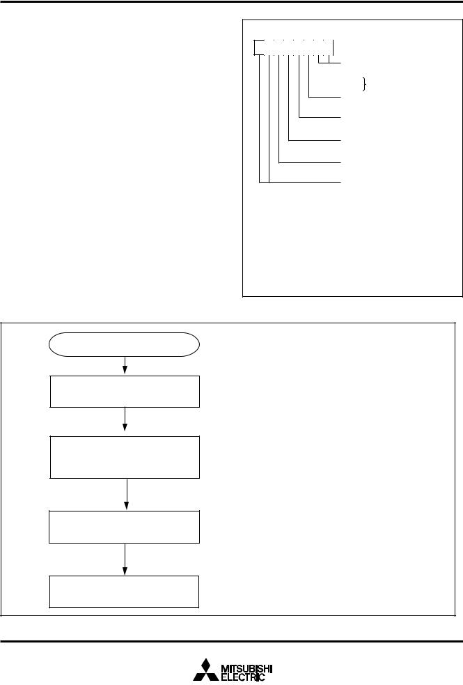
[CPU mode register] CPUM
The CPU mode register contains the stack page selection bit. This register is allocated at address 003B16.
Switching method of CPU mode register
Switch the CPU mode register (CPUM) at the head of program after releasing Reset in the following method.
b7 |
b0 |
CPU mode register
(CPUM: address 003B 16, initial value: 80 16)
Processor mode bits (Note 1) b1 b0
00 Single-chip mode
01
10 Not available
1 1
Stack page selection bit
0: 0 page
1: 1 page
Ring oscillator oscillation control bit
0: Ring oscillator oscillation enabled
1: Ring oscillator oscillation stop
XIN oscillation control bit
0: Ceramic or RC oscillation enabled
1: Ceramic or RC oscillation stop
Oscillation mode selection bit (Note 1)
0: Ceramic oscillation
1: RC oscillation
Clock division ratio selection bits
b7 |
b6 |
: f(φ ) = f(XIN)/2 (High-speed mode) |
0 |
0 |
|
0 |
1 |
: f(φ ) = f(XIN)/8 (Middle-speed mode) |
1 |
0 |
: applied from ring oscillator |
1 |
1 |
: f(φ ) = f(XIN) (Double-speed mode)(Note 2) |
Note 1: The bit can be rewritten only once after releasing reset. After rewriting it is disable to write any data to the bit. However, by reset the bit is initialized and can be rewritten, again.
(It is not disable to write any data to the bit for emulator MCU “M37540RSS”.)
2:These bits are used only when a ceramic oscillation is selected. Do not use these when an RC oscillation is selected.
Fig. 11 Structure of CPU mode register
After releasing reset |
Start with a built-in ring oscillator |
Switch the oscillation mode selection bit (bit 5 of CPUM)
Wait by ring oscillator operation until establishment of oscillator clock
Switch the clock division ratio selection bits (bits 6 and 7 of CPUM)
An initial value is set as a ceramic oscillation mode. When it is switched to an RC oscillation, its oscillation starts.
When using a ceramic oscillation, wait until establlishment of oscillation from oscillation starts. When using an RC oscillation, wait time is not required basically (time to execute the instruction to switch from a ring oscillator meets the requirement).
Select 1/1, 1/2, 1/8 or ring oscillator.
Main routine
Fig. 12 Switching method of CPU mode register
12

|
|
|
Y |
|
PRELIMINARThis |
|
|||
|
|
|
. . |
|
|
|
|
specification |
change |
|
|
|
to |
|
|
|
a |
final subject |
|
|
not |
are |
|
|
is |
|
|
||
|
limits |
|
||
|
|
|
|
|
Notice:parametric |
|
|
|
|
e |
|
|
|
|
Som |
|
|
|
|
MITSUBISHI MICROCOMPUTERS
7540 Group
SINGLE-CHIP 8-BIT CMOS MICROCOMPUTER
Memory
Special function register (SFR) area
The SFR area in the zero page contains control registers such as I/O ports and timers.
RAM
RAM is used for data storage and for a stack area of subroutine calls and interrupts.
Zero page
The 256 bytes from addresses 000016 to 00FF16 are called the zero page area. The internal RAM and the special function registers (SFR) are allocated to this area.
The zero page addressing mode can be used to specify memory and register addresses in the zero page area. Access to this area with only 2 bytes is possible in the zero page addressing mode.
Special page
ROM
The first 128 bytes and the last 2 bytes of ROM are reserved for device testing and the rest is a user area for storing programs.
Interrupt vector area
The interrupt vector area contains reset and interrupt vectors.
The 256 bytes from addresses FF0016 to FFFF16 are called the special page area. The special page addressing mode can be used to specify memory addresses in the special page area. Access to this area with only 2 bytes is possible in the special page addressing mode.
|
|
|
|
|
|
|
000016 |
|
|
|
|
|||||
|
|
|
|
|
|
|
SFR area |
|
|
|
||||||
|
|
|
|
|
|
|
|
|
|
|
|
|
|
|
|
|
|
|
|
|
|
|
|
|
|
|
|
|
|
|
|
|
Zero page |
|
|
|
|
|
|
|
004016 |
|
|
|
||||||
|
|
|
|
|
|
|
|
|
|
|
||||||
|
|
|
|
|
RAM |
010016 |
|
|
|
|
||||||
|
|
|
|
|
|
|
|
|
||||||||
|
|
|
|
|
|
|
|
|
|
|
|
|
|
|
||
|
|
|
RAM area |
|
|
|
|
|
|
|
|
|
|
|
|
|
|
|
|
|
|
|
|
|
|
|
|
|
|
|
|
||
|
|
|
RAM capacity |
address |
|
|
|
|
|
XXXX16 |
|
|
|
|
||
|
|
|
(bytes) |
XXXX16 |
|
|
|
|
|
|
|
|
|
|
|
|
|
|
|
|
|
|
|
|
|
|
|
|
|
|
|
|
|
|
|
|
512 |
023F16 |
|
|
|
|
|
|
|
|
Reserved area |
|
|
|
|
|
|
768 |
033F16 |
|
|
|
|
|
|
|
|
|
|
|
|
|
|
|
|
|
|
|
044016 |
|
|
|
|
|||||
|
|
|
|
|
|
|
Not used |
|
|
|
||||||
|
|
|
|
|
|
|
|
|
|
|
|
|
|
|
|
|
|
|
|
|
|
|
|
|
|
|
YYYY16 |
|
|
|
|
||
|
|
|
|
|
|
|
|
|
|
Reserved ROM area |
|
|
|
|||
|
|
|
|
|
|
|
|
|
|
|
|
|
|
|
|
|
|
|
|
|
|
|
|
|
|
|
|
|
|
(128 bytes) |
|
|
|
|
|
|
|
|
ROM |
|
|
|
ZZZZ16 |
|
|
|
|
|||
|
|
|
|
|
|
|
|
|
|
|
|
|||||
|
|
|
|
|
|
|
|
|
|
|
|
|
|
|
||
|
ROM area |
|
|
|
|
|
|
|
FF0016 |
|
|
|
|
|||
|
|
|
|
|
|
|
|
|
|
|
|
|||||
|
|
|
|
|
|
|
|
|
|
|
|
|
|
|
||
|
|
|
|
|
|
|
|
|
|
|
|
|
|
|
|
|
|
ROM capacity |
|
address |
address |
|
|
|
|
|
|
|
|
|
|
|
|
|
(bytes) |
|
YYYY16 |
ZZZZ16 |
|
|
|
|
|
FFDC16 |
|
|
|
Special page |
||
|
|
|
|
|
|
|
|
|
|
|
|
|
||||
|
16384 |
|
C00016 |
C08016 |
|
|
|
|
|
Interrupt vector area |
|
|
|
|||
|
|
|
|
|
|
|
|
|
|
|
|
|
||||
|
32768 |
|
800016 |
808016 |
|
|
|
|
|
FFFE16 |
|
|
|
|
||
|
|
|
|
|
|
|
|
|
|
Reserved ROM area |
|
|
|
|||
|
|
|
|
|
|
|
|
|
|
|||||||
|
|
|
|
|
|
|
|
|
|
FFFF16 |
|
|
|
|||
|
|
|
|
|
|
|
|
|
|
|
|
|
|
|||
|
|
|
|
|
|
|
|
|
|
|
|
|
|
|
|
|
Fig. 13 Memory map diagram |
|
|
|
|
|
|
|
|
|
|
|
|
|
|||
|
|
|
|
|
|
|
|
|
|
|
|
|
|
|
|
|
|
|
|
|
|
|
|
|
|
|
|
|
|
|
|
|
|
|
|
|
|
|
|
|
|
|
|
|
|
|
|
|
|
|
13

|
|
|
Y |
|
PRELIMINARThis |
|
|||
|
|
|
. . |
|
|
|
|
specification |
change |
|
|
|
to |
|
|
|
a |
final subject |
|
|
not |
are |
|
|
is |
|
|
||
|
limits |
|
||
|
|
|
|
|
Notice:parametric |
|
|
|
|
Some |
|
|
|
|
000016 Port P0 (P0)
000116 Port P0 direction register (P0D)
000216 Port P1 (P1)
000316 Port P1 direction register (P1D)
000416 Port P2 (P2)
000516 Port P2 direction register (P2D)
000616 Port P3 (P3)
000716 Port P3 direction register (P3D)
000816
000916
000A16
000B16
000C16
000D16
000E16
000F16
001016
001116
001216
001316
001416
001516
001616 Pull-up control register (PULL)
001716 Port P1P3 control register (P1P3C)
001816 Transmit/Receive buffer register (TB/RB)
001916 Serial I/O1 status register (SIO1STS)
001A16 Serial I/O1 control register (SIO1CON)
001B16 UART control register (UARTCON)
001C16 Baud rate generator (BRG)
001D16 Timer A mode register (TAM)
001E16 Timer A (low-order) (TAL)
001F16 Timer A (high-order) (TAH)
MITSUBISHI MICROCOMPUTERS
7540 Group
SINGLE-CHIP 8-BIT CMOS MICROCOMPUTER
002016 |
Timer Y, Z mode register (TYZM) |
|
|
002116 |
Prescaler Y (PREY) |
|
|
002216 |
Timer Y secondary (TYS) |
|
|
002316 |
Timer Y primary (TYP) |
|
|
002416 |
Timer Y, Z waveform output control register (PUM) |
|
|
002516 |
Prescaler Z (PREZ) |
|
|
002616 |
Timer Z secondary (TZS) |
|
|
002716 |
Timer Z primary (TZP) |
|
|
002816 |
Prescaler 1 (PRE1) |
|
|
002916 |
Timer 1 (T1) |
|
|
002A16 |
One-shot start register (ONS) |
|
|
002B16 |
Timer X mode register (TXM) |
|
|
002C16 |
Prescaler X (PREX) |
|
|
002D16 |
Timer X (TX) |
|
|
002E16 |
Timer count source set register (TCSS) |
002F16 |
|
|
|
|
|
003016 |
Serial I/O2 control register (SIO2CON) |
|
|
003116 |
Serial I/O2 register (SIO2) |
003216 |
|
|
|
003316 |
|
|
|
|
|
003416 |
A-D control register (ADCON) |
|
|
003516 |
A-D conversion register (low-order) (ADL) |
|
|
003616 |
A-D conversion register (high-order) (ADH) |
003716 |
|
|
|
|
|
003816 |
MISRG |
|
|
003916 |
Watchdog timer control register (WDTCON) |
|
|
003A16 |
Interrupt edge selection register (INTEDGE) |
|
|
003B16 |
CPU mode register (CPUM) |
|
|
003C16 |
Interrupt request register 1 (IREQ1) |
|
|
003D16 |
Interrupt request register 2 (IREQ2) |
|
|
003E16 |
Interrupt control register 1 (ICON1) |
|
|
003F16 |
Interrupt control register 2 (ICON2) |
|
|
Note : Do not access to the SFR area including nothing.
Fig. 14 Memory map of special function register (SFR)
14
|
|
|
Y |
|
PRELIMINARThis |
|
|||
|
|
|
. . |
|
|
|
|
specification |
change |
|
|
|
to |
|
|
|
a |
final subject |
|
|
not |
are |
|
|
is |
|
|
||
|
limits |
|
||
|
|
|
|
|
Notice:parametric |
|
|
|
|
e |
|
|
|
|
Som |
|
|
|
|
MITSUBISHI MICROCOMPUTERS
7540 Group
SINGLE-CHIP 8-BIT CMOS MICROCOMPUTER
I/O Ports
[Direction registers] PiD
The I/O ports have direction registers which determine the input/ output direction of each pin. Each bit in a direction register corresponds to one pin, and each pin can be set to be input or output.
When “1” is set to the bit corresponding to a pin, this pin becomes an output port. When “0” is set to the bit, the pin becomes an input port.
When data is read from a pin set to output, not the value of the pin itself but the value of port latch is read. Pins set to input are floating, and permit reading pin values.
If a pin set to input is written to, only the port latch is written to and the pin remains floating.
[Pull-up control register] PULL
By setting the pull-up control register (address 001616), ports P0 and P3 can exert pull-up control by program. However, pins set to output are disconnected from this control and cannot exert pull-up control.
[Port P1P3 control register] P1P3C
By setting the port P1P3 control register (address 001716), a CMOS input level or a TTL input level can be selected for ports
P10, P12, P13, P36, and P37 by program.
b7 |
b0 |
Pull-up control register
(PULL: address 0016 16, initial value: 00 16)
P00 pull-up control bit
P01 pull-up control bit P02, P03 pull-up control bit
P04 – P07 pull-up control bit P30 – P33 pull-up control bit P34 pull-up control bit
P35, P36 pull-up control bit P37 pull-up control bit
0 : Pull-up Off
1 : Pull-up On
Note 1: Pins set to output ports are disconnected from pull-up control.
2: Set the P35, P36 pull-up control bit to “1” (initial value: “0”) for 32-pin version.
Fig. 15 Structure of pull-up control register
|
b7 |
|
|
|
|
|
|
|
|
|
|
|
|
b0 |
|
|
|
|||||
|
|
|
|
|
|
|
|
|
|
|
|
|
|
|
|
|
Port P1P3 control register |
|||||
|
|
|
|
|
|
|
|
|
|
|
|
|
|
|
|
|
(P1P3C: address 0017 16, initial value: 00 16) |
|||||
|
|
|
|
|
|
|
|
|
|
|
|
|
|
|
|
|
|
|
|
|
|
|
|
|
|
|
|
|
|
|
|
|
|
|
|
|
|
|
|
|
|
|
|
|
|
|
|
|
|
|
|
|
|
|
|
|
|
|
|
|
|
|
|
P37/INT0 input level selection bit |
||||
|
|
|
|
|
|
|
|
|
|
|
|
|
|
|
|
|
|
|||||
|
|
|
|
|
|
|
|
|
|
|
|
|
|
|
0 |
: CMOS level |
|
|||||
|
|
|
|
|
|
|
|
|
|
|
|
|
|
|
1 |
: TTL level |
|
|||||
|
|
|
|
|
|
|
|
|
|
|
|
|
|
|
|
|
|
|
P36/INT1 input level selection bit |
|
||
|
|
|
|
|
|
|
|
|
|
|
|
|
|
|
|
|
|
|||||
|
|
|
|
|
|
|
|
|
|
|
|
|
0 |
: CMOS level |
|
|||||||
|
|
|
|
|
|
|
|
|
|
|
|
|
1 |
: TTL level |
|
|||||||
|
|
|
|
|
|
|
|
|
|
|
|
|
|
|
|
|
|
|
P10,P12,P13 input level selection bit |
|
||
|
|
|
|
|
|
|
|
|
|
|
|
|
|
|
|
|
|
|||||
|
|
|
|
|
|
|
|
|
|
|
0 |
: CMOS level |
|
|||||||||
|
|
|
|
|
|
|
|
|
|
|
1 |
: TTL level |
|
|||||||||
|
|
|
|
|
|
|
|
|
|
|
|
|
|
|
|
|
|
|
Not used |
|
||
|
|
|
|
|
|
|
|
|
|
|
|
|
|
|
|
|
|
|||||
|
|
|
||||||||||||||||||||
Note: Keep setting the P3 6/INT1 input level selection bit |
||||||||||||||||||||||
|
|
|
to “0” (initial value) for 32-pin version. |
|
|
|
||||||||||||||||
Fig. 16 Structure of port P1P3 control register
15

|
|
|
Y |
|
PRELIMINARThis |
|
|||
|
|
|
. . |
|
|
|
|
specification |
change |
|
|
|
to |
|
|
|
a |
final subject |
|
|
not |
are |
|
|
is |
|
|
||
|
limits |
|
||
|
|
|
|
|
Notice:parametric |
|
|
|
|
Some |
|
|
|
|
MITSUBISHI MICROCOMPUTERS
7540 Group
SINGLE-CHIP 8-BIT CMOS MICROCOMPUTER
Table 5 I/O port function table
Pin |
Name |
Input/output |
I/O format |
Non-port function |
Related SFRs |
Diagram No. |
P00/CNTR1 |
I/O port P0 |
I/O individual |
•CMOS compatible |
Key input interrupt |
Pull-up control register |
(1) |
P01/TYOUT |
|
bits |
input level |
Timer X function output |
Timer Y mode register |
(2) |
P02/TZOUT |
|
|
•CMOS 3-state output |
Timer Y function output |
Timer Z mode register |
(3) |
P03/TXOUT |
|
|
(Note 1) |
Timer Z function output |
Timer X mode register |
(4) |
P04–P07 |
|
|
Timer A function input |
Timer Y,Z waveform |
|
|
|
|
|
|
|||
|
|
|
|
|
output control register |
|
|
|
|
|
|
Timer A mode register |
|
P10/RxD1 |
I/O port P1 |
|
|
Serial I/O1 function |
Serial I/O1 control register |
(5) |
P11/TxD1 |
|
|
|
input/output |
|
(6) |
P12/SCLK1/SCLK2 |
|
|
|
Serial I/O2 function |
Serial I/O1 control register |
(7) |
P13/SRDY1/SDATA2 |
|
|
|
input/output |
Serial I/O2 control register |
(8) |
P14/CNTR0 |
|
|
|
Timer X function input/output |
Timer X mode register |
(9) |
P20/AN0– |
I/O port P2 |
|
|
A-D conversion input |
A-D control register |
(10) |
P27/AN7 |
(Note 2) |
|
|
|
|
|
|
|
|
|
|
|
|
P30–P35 |
I/O port P3 |
|
|
|
|
(11) |
P36/INT1 |
(Note 3) |
|
|
External interrupt input |
Interrupt edge selection |
(12) |
P37/INT0 |
|
|
|
|
register |
|
Notes 1: Ports P10, P12, P13, P36, and P37 are CMOS/TTL level.
2:P26/AN6 and P27/AN7 do not exist for the 32-pin version.
3:P35 and P36/INT1 do not exist for the 32-pin version.
16
|
|
|
Y |
|
PRELIMINARThis |
|
|||
|
|
|
. . |
|
|
|
|
specification |
change |
|
|
|
to |
|
|
|
a |
final subject |
|
|
not |
are |
|
|
is |
|
|
||
|
limits |
|
||
|
|
|
|
|
Notice:parametric |
|
|
|
|
e |
|
|
|
|
Som |
|
|
|
|
(1)Port P00
Data bus
Pull-up control
Direction |
|
|
register |
|
|
Port latch |
|
|
CNTR1 interrupt input |
|
|
To key input interrupt |
P00 key-on wakeup |
|
generating circuit |
||
selection bit |
||
|
(3)Port P03 |
|
|
Pull-up control |
|
Direction |
|
register |
Data bus |
Port latch |
|
Timer output |
|
P03/TXOUT |
|
output valid |
|
To key input interrupt |
|
generating circuit |
(5)Port P10
Serial I/O1 enable bit 
Receive enable bit 
|
Direction |
|
register |
Data bus |
Port latch |
Serial I/O1 input
(7)Port P12
P10, P12, P13 input level selection bit

 *
*
SCLK2 pin Serial I/O1 synchronous selection bit
clock selection bit Serial I/O1 enable bit 
Serial I/O1 mode selection bit 

Serial I/O1 enable bit 
|
Direction |
|
register |
Data bus |
Port latch |
|
P10, P12, P13 |
|
input level |
|
selection bit |
Serial I/O1, serial I/O2 clock output 

Serial I/O1, serial I/O2 clock input 
 *
*
MITSUBISHI MICROCOMPUTERS
7540 Group
SINGLE-CHIP 8-BIT CMOS MICROCOMPUTER
(2)Ports P01, P02 |
|
|
Pull-up control |
|
Direction |
|
register |
Data bus |
Port latch |
|
Pulse output mode |
|
Timer output |
|
To key input interrupt |
|
generating circuit |
(4)Ports P04–P07
Pull-up control |
Direction register
Data bus |
Port latch |
To key input interrupt generating circuit
(6)Port P11
P11/TxD1 P-channel output disable bit
Serial I/O1 enable bit 

Transmit enable bit 
Direction register
Data bus |
Port latch |
Serial I/O1 output
*P10, P12, P13, P36, and P37 input level are switched to the CMOS/TTL level by the port P1P3 control register. When the TTL level is selected, there is no hysteresis characteristics.
Fig. 17 Block diagram of ports (1)
17
|
|
|
Y |
|
PRELIMINARThis |
|
|||
|
|
|
. . |
|
|
|
|
specification |
change |
|
|
|
to |
|
|
|
a |
final subject |
|
|
not |
are |
|
|
is |
|
|
||
|
limits |
|
||
|
|
|
|
|
Notice:parametric |
|
|
|
|
Some |
|
|
|
|
MITSUBISHI MICROCOMPUTERS
7540 Group
SINGLE-CHIP 8-BIT CMOS MICROCOMPUTER
(8) Port P13
SDATA2 output in operation signal |
|
SDATA2 pin selection bit |
|
Serial I/O mode selection bit |
|
Serial I/O1 enable bit |
|
SRDY1 output enable bit |
|
|
Direction |
|
register |
Data bus |
Port latch |
|
P10, P12, P13 |
|
input level |
|
selection bit |
|
Serial I/O1 ready output |
|
Serial I/O2 output |
|
Serial I/O2 input |
|
* |
(10) Ports P20–P27 |
|
|
Direction |
|
register |
Data bus |
Port latch |
A-D converter input

 Analog input pin selection bit
(12) Ports P36, P37
Pull-up control |
|
Direction |
|
register |
Data bus |
Port latch |
INT interrupt input
P3 input level selection bit

 *
*
(9) Port P14
|
Direction |
|
register |
Data bus |
Port latch |
|
Pulse output mode |
|
Timer output |
|
CNTR0 interrupt input |
(11) Ports P30–P35
Pull-up control |
|
Direction |
|
register |
Data bus |
Port latch |
* P10, P12, P13, P36, and P37 input level are switched to the CMOS/TTL level by the port P1P3 control register. When the TTL level is selected, there is no hysteresis characteristics.
Fig. 18 Block diagram of ports (2)
18

|
|
|
Y |
|
PRELIMINARThis |
|
|||
|
|
|
. . |
|
|
|
|
specification |
change |
|
|
|
to |
|
|
|
a |
final subject |
|
|
not |
are |
|
|
is |
|
|
||
|
limits |
|
||
|
|
|
|
|
Notice:parametric |
|
|
|
|
e |
|
|
|
|
Som |
|
|
|
|
MITSUBISHI MICROCOMPUTERS
7540 Group
SINGLE-CHIP 8-BIT CMOS MICROCOMPUTER
Interrupts
Interrupts occur by 15 different sources : 5 external sources, 9 internal sources and 1 software source.
Interrupt control
All interrupts except the BRK instruction interrupt have an interrupt request bit and an interrupt enable bit, and they are controlled by the interrupt disable flag. When the interrupt enable bit and the interrupt request bit are set to “1” and the interrupt disable flag is set to “0”, an interrupt is accepted.
The interrupt request bit can be cleared by program but not be set.
The interrupt enable bit can be set and cleared by program.
The reset and BRK instruction interrupt can never be disabled with any flag or bit. All interrupts except these are disabled when the interrupt disable flag is set.
When several interrupts occur at the same time, the interrupts are received according to priority.
Table 6 Interrupt vector address and priority
Interrupt operation
Upon acceptance of an interrupt the following operations are automatically performed:
1.The processing being executed is stopped.
2.The contents of the program counter and processor status register are automatically pushed onto the stack.
3.The interrupt disable flag is set and the corresponding interrupt request bit is cleared.
4.Concurrently with the push operation, the interrupt destination address is read from the vector table into the program counter.
Notes on use
When the active edge of an external interrupt (INT 0, INT1,CNTR0,CNTR1) is set, the interrupt request bit may be set to “1”. Related register: Interrupt edge selection register (address 003A16)
When not requiring the interrupt occurrence synchronized with this setting, take following sequence:
1.Clear the interrupt enable bit to “0” (disabled).
2.Set the interrupt edge selection bit to “1”.
3.Clear the interrupt request bit to “0” after 1 or more instructions have been executed.
4.Set the interrupt enable bit to “1” (enabled).
Interrupt source |
Priority |
Vector addresses (Note 1) |
Interrupt request generating conditions |
Remarks |
||
|
|
|||||
High-order |
Low-order |
|||||
|
|
|
|
|
|
|
Reset (Note 2) |
1 |
FFFD16 |
FFFC16 |
At reset input |
Non-maskable |
|
Serial I/O1 receive |
2 |
FFFB16 |
FFFA16 |
At completion of serial I/O1 data receive |
Valid only when serial I/O1 is selected |
|
|
|
|
|
|
|
|
Serial I/O1 transmit |
3 |
FFF916 |
FFF816 |
At completion of serial I/O1 transmit shift or |
Valid only when serial I/O1 is |
|
|
|
|
|
when transmit buffer is empty |
selected |
|
INT0 |
4 |
FFF716 |
FFF616 |
At detection of either rising or falling edge of |
External interrupt |
|
|
|
|
|
INT0 input |
(active edge selectable) |
|
|
|
|
|
|
|
|
INT1 (Note 3) |
5 |
FFF516 |
FFF416 |
At detection of either rising or falling edge of |
External interrupt |
|
|
|
|
|
INT1 input |
(active edge selectable) |
|
|
|
|
|
|
|
|
Key-on wake-up |
6 |
FFF316 |
FFF216 |
At falling of conjunction of input logical level |
External interrupt (valid at falling) |
|
|
|
|
|
for port P0 (at input) |
|
|
CNTR0 |
7 |
FFF116 |
FFF016 |
At detection of either rising or falling edge of |
External interrupt |
|
|
|
|
|
CNTR0 input |
(active edge selectable) |
|
|
|
|
|
|
|
|
CNTR1 |
8 |
FFEF16 |
FFEE16 |
At detection of either rising or falling edge of |
External interrupt |
|
|
|
|
|
CNTR1 input |
(active edge selectable) |
|
|
|
|
|
|
|
|
Timer X |
9 |
FFED16 |
FFEC16 |
At timer X underflow |
|
|
Timer Y |
10 |
FFEB16 |
FFEA16 |
At timer Y underflow |
|
|
Timer Z |
11 |
FFE916 |
FFE816 |
At timer Z underflow |
|
|
Timer A |
12 |
FFE716 |
FFE616 |
At timer A underflow |
|
|
|
|
|
|
|
|
|
Serial I/O2 |
13 |
FFE516 |
FFE416 |
At completion of transmit/receive shift |
|
|
A-D conversion |
14 |
FFE316 |
FFE216 |
At completion of A-D conversion |
|
|
Timer 1 |
15 |
FFE116 |
FFE016 |
At timer 1 underflow |
STP release timer underflow |
|
Reserved area |
16 |
FFDF16 |
FFDE16 |
Not available |
|
|
BRK instruction |
17 |
FFDD16 |
FFDC16 |
At BRK instruction execution |
Non-maskable software interrupt |
|
Note 1: Vector addressed contain internal jump destination addresses.
2:Reset function in the same way as an interrupt with the highest priority.
3:It is an interrupt which can use only for 36 pin version.
19
|
|
|
Y |
|
PRELIMINARThis |
|
|||
|
|
|
. . |
|
|
|
|
specification |
change |
|
|
|
to |
|
|
|
a |
final subject |
|
|
not |
are |
|
|
is |
|
|
||
|
limits |
|
||
|
|
|
|
|
Notice:parametric |
|
|
|
|
Some |
|
|
|
|
MITSUBISHI MICROCOMPUTERS
7540 Group
SINGLE-CHIP 8-BIT CMOS MICROCOMPUTER
Interrupt request bit
Interrupt enable bit
Interrupt disable flag I
BRK instruction |
|
|
|
|
|
Interrupt request |
|
|
|
||||
Reset |
|
|
|
|
|
|
|
|
|
|
|
|
Fig. 19 Interrupt control
|
b7 |
|
b0 |
|
Interrupt edge selection register |
|
|
|
|
|
||||||||||||||||||
|
|
|
|
|
|
|
|
|
|
|
|
|
|
|
|
|
|
(INTEDGE : address 003A16, initial value : 0016) |
|
|
|
|
||||||
|
|
|
|
|
|
|
|
|
|
|
|
|
|
|
|
|
|
|
|
|
|
|
|
|
|
|
|
|
|
|
|
|
|
|
|
|
|
|
|
|
|
|
|
|
|
|
|
|
|
|
INT0 interrupt edge selection bit |
|
|
|
|
||
|
|
|
|
|
|
|
|
|
|
|
|
|
|
|
|
|
|
|
|
|
|
|
|
|
||||
|
|
|
|
|
|
|
|
|
|
|
|
|
|
|
|
|
|
|
|
|
|
0 : Falling edge active |
|
|
|
|
||
|
|
|
|
|
|
|
|
|
|
|
|
|
|
|
|
|
|
|
|
|
|
1 : Rising edge active |
|
|
|
|
||
|
|
|
|
|
|
|
|
|
|
|
|
|
|
|
|
|
|
|
|
|
|
INT1 interrupt edge selection bit |
|
|
|
|
||
|
|
|
|
|
|
|
|
|
|
|
|
|
|
|
|
|
|
|
|
|
|
|
|
|
|
|||
|
|
|
|
|
|
|
|
|
|
|
|
|
|
|
|
|
|
|
|
|
|
0 : Falling edge active |
|
|
|
|
||
|
|
|
|
|
|
|
|
|
|
|
|
|
|
|
|
|
|
|
|
|
|
1 : Rising edge active |
|
|
|
|
||
|
|
|
|
|
|
|
|
|
|
|
|
|
|
|
|
|
|
|
|
|
|
Not used (returns “0” when read) |
|
|
|
|
||
|
|
|
|
|
|
|
|
|
|
|
|
|
|
|
|
|
|
|
|
|
|
|
|
|
||||
|
|
|
|
|
|
|
|
|
|
|
|
|
|
|
|
|
|
|
|
|
|
P00 key-on wakeup enable bit |
|
|
|
|
||
|
|
|
|
|
|
|
|
|
|
|
|
|
|
|
|
|
|
|
|
|
|
0 : Key-on wakeup enabled |
|
|
|
|
||
|
|
|
|
|
|
|
|
|
|
|
|
|
|
|
|
|
|
|
|
|
|
1 : Key-on wakeup disabled |
|
|
|
|
||
|
|
|
|
|
|
|
|
|
|
|
|
|
|
|
|
|
|
|
|
|
|
|
|
|
|
|
|
|
b7 |
|
b0 |
|
|
|
|
|
|
|
|
|
|||||||||||||||||
|
|
|
Interrupt request register 1 |
|
|
|
|
|||||||||||||||||||||
|
|
|
|
|
|
|
|
|
|
|
|
|
|
|
|
|
|
(IREQ1 : address 003C16, initial value : 0016) |
|
|
|
|
||||||
|
|
|
|
|
|
|
|
|
|
|
|
|
|
|
|
|
|
|
|
|
|
|
|
|
|
|
||
|
|
|
|
|
|
|
|
|
|
|
|
|
|
|
|
|
|
|
|
|
|
Serial I/O1 receive interrupt request bit |
|
|
|
|
||
|
|
|
|
|
|
|
|
|
|
|
|
|
|
|
|
|
|
|
|
|
|
|
|
|
|
|||
|
|
|
|
|
|
|
|
|
|
|
|
|
|
|
|
|
|
|
|
|
|
Serial I/O1 transmit interrupt request bit |
|
|
|
|
||
|
|
|
|
|
|
|
|
|
|
|
|
|
|
|
|
|
|
|
|
|
|
|
|
|
|
|||
|
|
|
|
|
|
|
|
|
|
|
|
|
|
|
|
|
|
|
|
|
|
INT0 interrupt request bit |
|
|
|
|
||
|
|
|
|
|
|
|
|
|
|
|
|
|
|
|
|
|
|
|
|
|
|
|
|
|
|
|||
|
|
|
|
|
|
|
|
|
|
|
|
|
|
|
|
|
|
|
|
|
|
INT1 interrupt request bit |
|
|
|
|
||
|
|
|
|
|
|
|
|
|
|
|
|
|
|
|
|
|
|
|
|
|
|
|
|
|
|
|||
|
|
|
|
|
|
|
|
|
|
|
|
|
|
|
|
|
|
|
|
|
|
Key-on wake up interrupt request bit |
|
|
|
|
||
|
|
|
|
|
|
|
|
|
|
|
|
|
|
|
|
|
|
|
|
|
|
|
|
|
|
|||
|
|
|
|
|
|
|
|
|
|
|
|
|
|
|
|
|
|
|
|
|
|
CNTR0 interrupt request bit |
|
|
|
|
||
|
|
|
|
|
|
|
|
|
|
|
|
|
|
|
|
|
|
|
|
|
|
|
|
|
|
|||
|
|
|
|
|
|
|
|
|
|
|
|
|
|
|
|
|
|
|
|
|
|
CNTR1 interrupt request bit |
|
|
|
|||
|
|
|
|
|
|
|
|
|
|
|
|
|
|
|
|
|
|
|
|
|
|
|
0 : No interrupt request issued |
|||||
|
|
|
|
|
|
|
|
|
|
|
|
|
|
|
|
|
|
|
|
|
|
|||||||
|
|
|
|
|
|
|
|
|
|
|
|
|
|
|
|
|
|
|
|
|
|
Timer X interrupt request bit |
|
1 : Interrupt request issued |
||||
|
|
|
|
|
|
|
|
|
|
|
|
|
|
|
|
|
|
|
|
|
|
|||||||
|
|
|
|
|
|
|
|
|
|
|
|
|
|
|
|
|
|
|
|
|
|
|
|
|
|
|
|
|
|
|
|
|
|
|
|
|
|
|
|
|
|
|
|
|
|
|
|
|
|
|
|
|
|
|
|
|
|
b7 |
|
b0 |
|
|
|
|
|
|
|
|
||||||||||||||||||
|
|
|
Interrupt request register 2 |
|
|
|
|
|||||||||||||||||||||
|
|
|
|
|
|
|
|
|
|
|
|
|
|
|
|
|
|
(IREQ2 : address 003D16, initial value : 0016) |
|
|
|
|
||||||
|
|
|
|
|
|
|
|
|
|
|
|
|
|
|
|
|
|
|
|
|
|
|
|
|
|
|
||
|
|
|
|
|
|
|
|
|
|
|
|
|
|
|
|
|
|
|
|
|
|
Timer Y interrupt request bit |
|
|
|
|
||
|
|
|
|
|
|
|
|
|
|
|
|
|
|
|
|
|
|
|
|
|
|
|
|
|
|
|||
|
|
|
|
|
|
|
|
|
|
|
|
|
|
|
|
|
|
|
|
|
|
Timer Z interrupt request bit |
|
|
|
|
||
|
|
|
|
|
|
|
|
|
|
|
|
|
|
|
|
|
|
|
|
|
|
|
|
|
|
|||
|
|
|
|
|
|
|
|
|
|
|
|
|
|
|
|
|
|
|
|
|
|
Timer A interrupt request bit |
|
|
|
|
||
|
|
|
|
|
|
|
|
|
|
|
|
|
|
|
|
|
|
|
|
|
|
|
|
|
|
|||
|
|
|
|
|
|
|
|
|
|
|
|
|
|
|
|
|
|
|
|
|
|
Serial I/O2 interrupt request bit |
|
|
|
|
||
|
|
|
|
|
|
|
|
|
|
|
|
|
|
|
|
|
|
|
|
|
|
|
|
|
|
|||
|
|
|
|
|
|
|
|
|
|
|
|
|
|
|
|
|
|
|
|
|
|
A-D conversion interrupt request bit |
|
|
|
|
||
|
|
|
|
|
|
|
|
|
|
|
|
|
|
|
|
|
|
|
|
|
|
|
|
|
|
|||
|
|
|
|
|
|
|
|
|
|
|
|
|
|
|
|
|
|
|
|
|
|
Timer 1 interrupt request bit |
|
|
|
|
||
|
|
|
|
|
|
|
|
|
|
|
|
|
|
|
|
|
|
|
|
|
|
|
|
|
|
|||
|
|
|
|
|
|
|
|
|
|
|
|
|
|
|
|
|
|
|
|
|
|
Not used (returns “0” when read) |
|
|
||||
|
|
|
|
|
|
|
|
|
|
|
|
|
|
|
|
|
|
|
|
|
|
|
0 : No interrupt request issued |
|||||
|
|
|
|
|
|
|
|
|
|
|
|
|
|
|
|
|
|
|
|
|
|
|||||||
|
|
|
|
|
|
|
|
|
|
|
|
|
|
|
|
|
|
|
|
|
|
|
|
|
|
1 : Interrupt request issued |
||
|
|
|
|
|
|
|
|
|
|
|
|
|
|
|
|
|
|
|
|
|
|
|
|
|
|
|
|
|
b7 |
|
b0 |
|
|
|
|
|
|
|
|
||||||||||||||||||
|
|
|
Interrupt control register 1 |
|
|
|
|
|||||||||||||||||||||
|
|
|
|
|
|
|
|
|
|
|
|
|
|
|
|
|
|
(ICON1 : address 003E16, initial value : 0016) |
|
|
|
|
||||||
|
|
|
|
|
|
|
|
|
|
|
|
|
|
|
|
|
|
|
|
|
|
|
|
|
|
|
||
|
|
|
|
|
|
|
|
|
|
|
|
|
|
|
|
|
|
|
|
|
|
Serial I/O1 receive interrupt enable bit |
|
|
|
|
||
|
|
|
|
|
|
|
|
|
|
|
|
|
|
|
|
|
|
|
|
|
|
|
|
|
|
|||
|
|
|
|
|
|
|
|
|
|
|
|
|
|
|
|
|
|
|
|
|
|
Serial I/O1 transmit interrupt enable bit |
|
|
|
|
||
|
|
|
|
|
|
|
|
|
|
|
|
|
|
|
|
|
|
|
|
|
|
|
|
|
|
|||
|
|
|
|
|
|
|
|
|
|
|
|
|
|
|
|
|
|
|
|
|
|
INT0 interrupt enable bit |
|
|
|
|
||
|
|
|
|
|
|
|
|
|
|
|
|
|
|
|
|
|
|
|
|
|
|
|
|
|
|
|||
|
|
|
|
|
|
|
|
|
|
|
|
|
|
|
|
|
|
|
|
|
|
INT1 interrupt enable bit (Do not write “1” to this bit for 32-pin version) |
|
|||||
|
|
|
|
|
|
|
|
|
|
|
|
|
|
|
|
|
|
|
|
|
|
|||||||
|
|
|
|
|
|
|
|
|
|
|
|
|
|
|
|
|
|
|
|
|
|
Key-on wake up interrupt enable bit |
|
|
|
|
||
|
|
|
|
|
|
|
|
|
|
|
|
|
|
|
|
|
|
|
|
|
|
|
|
|
|
|||
|
|
|
|
|
|
|
|
|
|
|
|
|
|
|
|
|
|
|
|
|
|
CNTR0 interrupt enable bit |
|
|
|
|
||
|
|
|
|
|
|
|
|
|
|
|
|
|
|
|
|
|
|
|
|
|
|
|
|
|
|
|||
|
|
|
|
|
|
|
|
|
|
|
|
|
|
|
|
|
|
|
|
|
|
CNTR1 interrupt enable bit |
|
|
|
|
||
|
|
|
|
|
|
|
|
|
|
|
|
|
|
|
|
|
|
|
|
|
|
|
|
|
|
|||
|
|
|
|
|
|
|
|
|
|
|
|
|
|
|
|
|
|
|
|
|
|
Timer X interrupt enable bit |
|
0 : Interrupts disabled |
|
|||
|
|
|
|
|
|
|
|
|
|
|
|
|
|
|
|
|
|
|
|
|
|
|
||||||
|
|
|
|
|
|
|
|
|
|
|
|
|
|
|
|
|
|
|
|
|
|
|
|
|
|
1 : Interrupts enabled |
|
|
|
|
|
|
|
|
|
|
|
|
|
||||||||||||||||||
b7 |
|
b0 |
|
|
|
|
|
|
|
|
||||||||||||||||||
|
|
|
Interrupt control register 2 |
|
|
|
|
|||||||||||||||||||||
|
|
|
|
|
|
|
|
|
|
|
|
|
|
|
|
|
|
(ICON2 : address 003F16, initial value : 0016) |
|
|
|
|
||||||
|
|
|
|
|
|
|
|
|
|
|
|
|
|
|
|
|
|
|
|
|
|
|
|
|
|
|
||
|
|
|
|
|
|
|
|
|
|
|
|
|
|
|
|
|
|
|
|
|
|
Timer Y interrupt enable bit |
|
|
|
|
||
|
|
|
|
|
|
|
|
|
|
|
|
|
|
|
|
|
|
|
|
|
|
|
|
|
|
|||
|
|
|
|
|
|
|
|
|
|
|
|
|
|
|
|
|
|
|
|
|
|
Timer Z interrupt enable bit |
|
|
|
|
||
|
|
|
|
|
|
|
|
|
|
|
|
|
|
|
|
|
|
|
|
|
|
|
|
|
|
|||
|
|
|
|
|
|
|
|
|
|
|
|
|
|
|
|
|
|
|
|
|
|
Timer A interrupt enable bit |
|
|
|
|
||
|
|
|
|
|
|
|
|
|
|
|
|
|
|
|
|
|
|
|
|
|
|
|
|
|
|
|||
|
|
|
|
|
|
|
|
|
|
|
|
|
|
|
|
|
|
|
|
|
|
Serial I/O2 interrupt enable bit |
|
|
|
|
||
|
|
|
|
|
|
|
|
|
|
|
|
|
|
|
|
|
|
|
|
|
|
|
|
|
|
|||
|
|
|
|
|
|
|
|
|
|
|
|
|
|
|
|
|
|
|
|
|
|
A-D conversion interrupt enable bit |
|
|
|
|
||
|
|
|
|
|
|
|
|
|
|
|
|
|
|
|
|
|
|
|
|
|
|
|
|
|
|
|||
|
|
|
|
|
|
|
|
|
|
|
|
|
|
|
|
|
|
|
|
|
|
Timer 1 interrupt enable bit |
|
|
|
|
||
|
|
|
|
|
|
|
|
|
|
|
|
|
|
|
|
|
|
|
|
|
|
|
|
|
|
|||
|
|
|
|
|
|
|
|
|
|
|
|
|
|
|
|
|
|
|
|
|
|
Not used (returns “0” when read) |
|
0 : Interrupts disabled |
|
|||
|
|
|
|
|
|
|
|
|
|
|
|
|
|
|
|
|
|
|
|
|
|
|
|
|||||
|
|
|
|
|
|
|
|
|
|
|
|
|
|
|
|
|
|
|
|
|
|
|
||||||
|
|
|
|
|
|
|
|
|
|
|
|
|
|
|
|
|
|
|
|
|
|
(Do not write “1” to this bit) |
|
1 : Interrupts enabled |
|
|||
|
|
|
|
|
|
|
|
|
|
|
|
|
|
|
|
|
|
|
|
|
|
|
|
|
|
|
|
|
Fig. 20 Structure of Interrupt-related registers
20
|
|
|
Y |
|
PRELIMINARThis |
|
|||
|
|
|
. . |
|
|
|
|
specification |
change |
|
|
|
to |
|
|
|
a |
final subject |
|
|
not |
are |
|
|
is |
|
|
||
|
limits |
|
||
|
|
|
|
|
Notice:parametric |
|
|
|
|
e |
|
|
|
|
Som |
|
|
|
|
Key Input Interrupt (Key-On Wake-Up)
MITSUBISHI MICROCOMPUTERS
7540 Group
SINGLE-CHIP 8-BIT CMOS MICROCOMPUTER
A key-on wake-up interrupt request is generated by applying “L” level to any pin of port P0 that has been set to input mode.
In other words, it is generated when the AND of input level goes from “1” to “0”. An example of using a key input interrupt is shown in Figure 21, where an interrupt request is generated by pressing one of the keys provided as an active-low key matrix which uses ports P00 to P03 as input ports.
Port PXx |
|
|
|
“L” level output |
|
|
|
|
PULL register |
Port P07 |
|
|
bit 3 = “0” |
|
|
|
Direction register = “1” |
|
|
|
|
|
|
* |
** |
Port P07 |
Key input interrupt request |
P07 output |
|
latch |
|
|
Falling edge |
|
|
|
|
detection |
|
|
PULL register |
Port P06 |
|
|
bit 3 = “0” |
|
|
|
Direction register = “1” |
|
|
|
|
|
|
* |
** |
Port P06 |
|
P06 output |
|
latch |
|
|
Falling edge |
|
|
|
|
detection |
|
|
PULL register |
Port P05 |
|
|
bit 3 = “0” |
|
|
|
Direction register = “1” |
|
|
|
|
|
|
* |
** |
Port P05 |
|
P05 output |
|
latch |
|
|
Falling edge |
|
|
|
|
detection |
|
|
PULL register |
Port P04 |
|
|
bit 3 = “0” |
|
|
|
Direction register = “1” |
|
|
|
|
|
|
* |
** |
Port P04 |
|
P04 output |
|
latch |
|
|
Falling edge |
|
|
|
|
detection |
|
|
PULL register |
Port P03 |
|
|
bit 2 = “1” |
Port P0 |
|
|
|
Direction register = “0” |
|
* |
** |
Port P03 |
Input read circuit |
P03 input |
|
latch |
|
|
Falling edge |
|
|
|
|
detection |
|
|
PULL register |
Port P02 |
|
|
bit 2 = “1” |
|
|
|
|
Direction register = “0” |
|
* |
** |
Port P02 |
|
P02 input |
|
latch |
|
|
Falling edge |
|
|
|
|
detection |
|
|
PULL register |
Port P01 |
|
|
bit 1 = “1” |
|
|
|
|
Direction register = “0” |
|
* |
** |
Port P01 |
|
P01 input |
|
latch |
|
|
Falling edge |
|
|
|
|
detection |
|
|
PULL register |
Port P00 |
|
|
bit 0 = “1” |
|
|
|
|
Direction register = “0” |
|
* |
** |
Port P00 |
|
P00 input |
|
latch |
|
|
Falling edge |
|
|
|
|
detection |
|
Port P00 key-on wakeup |
|
|
|
selection bit |
* P-channel transistor for pull-up |
||
|
|
||
|
|
** CMOS output buffer |
|
Fig. 21 Connection example when using key input interrupt and port P0 block diagram
21

|
|
|
Y |
|
PRELIMINARThis |
|
|||
|
|
|
. . |
|
|
|
|
specification |
change |
|
|
|
to |
|
|
|
a |
final subject |
|
|
not |
are |
|
|
is |
|
|
||
|
limits |
|
||
|
|
|
|
|
Notice:parametric |
|
|
|
|
Some |
|
|
|
|
MITSUBISHI MICROCOMPUTERS
7540 Group
SINGLE-CHIP 8-BIT CMOS MICROCOMPUTER
Timers
The 7540 Group has 5 timers: timer 1, timer A, timer X, timer Y and timer Z.
The division ratio of every timer and prescaler is 1/(n+1) provided that the value of the timer latch or prescaler is n.
All the timers are down count timers. When a timer reaches “0”, an underflow occurs at the next count pulse, and the corresponding timer latch is reloaded into the timer. When a timer underflows, the interrupt request bit corresponding to each timer is set to “1”.
●Timer 1
Timer 1 is an 8-bit timer and counts the prescaler output.
When Timer 1 underflows, the timer 1 interrupt request bit is set to “1”.
Prescaler 1 is an 8-bit prescaler and counts the signal which is the oscillation frequency divided by 16.
Prescaler 1 and Timer 1 have the prescaler 1 latch and the timer 1 latch to retain the reload value, respectively. The value of prescaler 1 latch is set to Prescaler 1 when Prescaler 1 underflows.The value of timer 1 latch is set to Timer 1 when Timer
1 underflows.
When writing to Prescaler 1 (PRE1) is executed, the value is written to both the prescaler 1 latch and Prescaler 1.
When writing to Timer 1 (T1) is executed, the value is written to both the timer 1 latch and Timer 1.
When reading from Prescaler 1 (PRE1) and Timer 1 (T1) is executed, each count value is read out.
Timer 1 always operates in the timer mode.
Prescaler 1 counts the selected count source. Each time the count clock is input, the contents of Prescaler 1 is decremented by 1. When the contents of Prescaler 1 reach “0016”, an underflow occurs at the next count clock, and the prescaler 1 latch is reloaded into Prescaler 1 and count continues. The division ratio of
Prescaler 1 is 1/(n+1) provided that the value of Prescaler 1 is n.
The contents of Timer 1 is decremented by 1 each time the underflow signal of Prescaler 1 is input. When the contents of Timer 1 reach “0016”, an underflow occurs at the next count clock, and the timer 1 latch is reloaded into Timer 1 and count continues. The division ratio of Timer 1 is 1/(m+1) provided that the value of Timer
1 is m. Accordingly, the division ratio of Prescaler 1 and Timer 1 is
1/((n+1) (m+1)) provided that the value of Prescaler 1 is n and the value of Timer 1 is m.
Timer 1 cannot stop counting by software.
22
Loading...