


M37471M8-XXXFP
Table of contents
 Loading...
Mitsubishi M37471M8-XXXFP, M37471M4-XXXSP, M37471M4-XXXFP, M37471M2-XXXSP, M37471M2-XXXFP Datasheet
...
1
2
3
4
5
6
7
8
9
10
11
12
13
14
15
16
17
18
19
20
21
22
23
24
25
26
27
28
29
30
31
32
M37470M2-XXXSP
M37470M4-XXXSP
M37470E4-XXXSP
M37470M8-XXXSP
M37470E8-XXXSP
P07
P06
P05
P04
P03
P02
P01
P00
P41
P40
P33/CNTR1
P32/CNTR0
P31/INT1
P30/INT0
RESET
V
CC
P16/CLK
P1
5/SOUT
P14/SIN
P13/
P1
1
P10
P23/IN3
P22/IN2
P21/IN1
P20/IN0
VREF
XIN
XOUT
VSS
P17/SRDY
Outline 32P4B
T1
P12/T0
DESCRIPTION
The 7470/7471 group is a single-chip microcomputer designed
with CMOS silicon gate technology. It is housed in a 32-pin shrink
plastic molded DIP. The M37471M2-XXXSP/FP is a single-chip mi-
crocomputer designed with CMOS silicon gate technology. It is
housed in a 42-pin shrink plastic molded DIP or a 56-pin plastic
molded QFP.
These single-chip microcomputer are useful for business equip-
ment and other consumer applications.
In addition to its simple instruction set, the ROM, RAM, and I/O
addresses are placed on the same memory map to enable easy
programming .
The differences between the M37471M2-XXXSP and the
M37471M2-XXXFP are the package outline and the power dissi-
pation ability (absolute maximum ratings).
The differences among M37470M2-XXXSP, M37470M4-XXXSP,
M37470M8-XXXSP, M37471M2-XXXSP/FP, M37471M4-XXXSP/
FP and M37471M8-XXXSP/FP are noted below.
APPLICATION
Audio-visual equipment, VCR, Tuner,
Office automation equipment
7470/7471 Group
SINGLE-CHIP 8-BIT CMOS MICROCOMPUTER
MITSUBISHI MICROCOMPUTERS
Type name
M37470M2-XXXSP
M37471M2-XXXSP/FP
M37470M4-XXXSP
M37471M4-XXXSP/FP
M37470M8-XXXSP
M37471M8-XXXSP/FP
I/O ports
26
36
26
36
26
36
ROM size
4096 bytes
8192 bytes
16384 bytes
RAM size
128 bytes
192 bytes
384 bytes
FEATURES
●Basic machine-language instructions ...................................... 71
●Memory size
ROM ..................................................... 4096 bytes (M37471M2)
RAM........................................................ 128 bytes (M37471M2)
●The minimum instruction execution time
....................................... 0.5 µs (at 8 MHz oscillation frequency)
●Power source voltage
.............. 2.7 to 4.5 V (at 2.2V
CC–2.0 MHz oscillation frequency)
...............................4.5 to 5.5 V (at 8 MHz oscillation frequency)
●Power dissipation in normal mode
...................................35 mW (at 8.0 MHz oscillation frequency)
●Subroutine nesting ......64 levels max. (M37470M2, M37471M2)
●Interrupt ................................................... 12 sources, 10 vectors
●8-bit timers .................................................................................. 4
●Programmable I/O ports
(Ports P0, P1, P2, P4).........................................22(7470 group)
28(7471 group)
●Input port (Port P3) ............................................... 4(7470 group)
(Ports P3, P5)....................................... 8(7471 group)
●Serial I/O (8-bit) .......................................................................... 1
● A-D converter ............................... 8-bit, 4channels (7470 group)
8-bit, 8channels (7471 group)
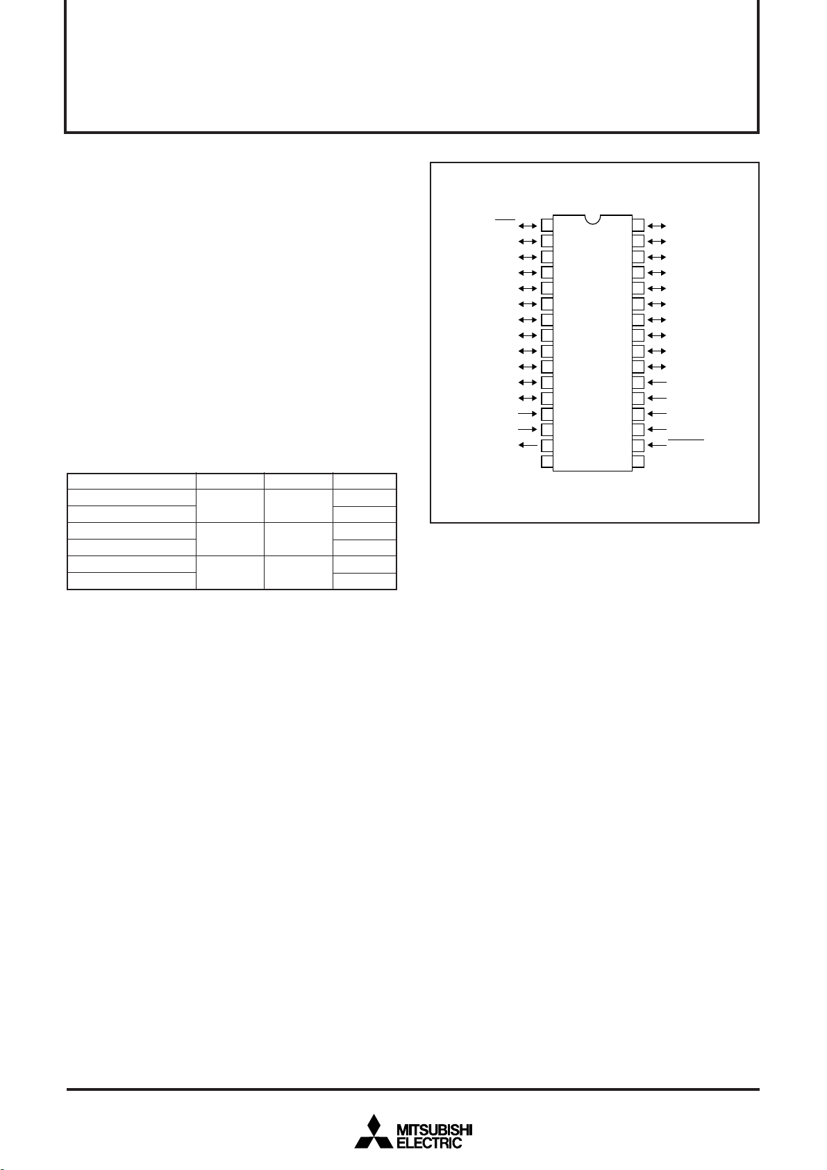
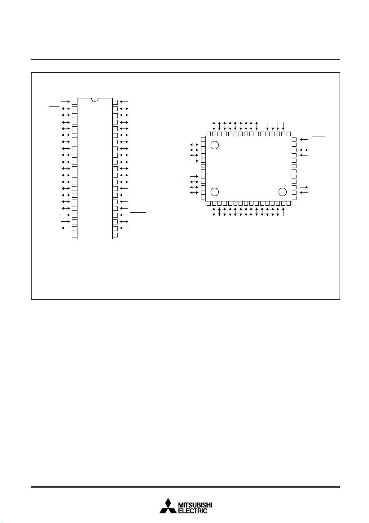
PIN CONFIGURATION (TOP VIEW)
2
7470/7471 Group
SINGLE-CHIP 8-BIT CMOS MICROCOMPUTER
MITSUBISHI MICROCOMPUTERS
PIN CONFIGURATION (TOP VIEW)
P13/T1
P12/T0
1
2
3
4
5
6
7
8
9
10
11
12
13
14
15
16
42
41
40
39
38
37
36
35
34
33
32
31
30
29
28
27
M37471M2-XXXSP
M37471M4-XXXSP
M37471E4-XXXSP
M37471M8-XXXSP
M37471E8-XXXSP
M37471E8SS
17
18
19
20
21
26
25
24
23
22
P53
P16/CLK
P1
5/SOUT
P14/SIN
P11
P10
P27/IN7
P26/IN6
P25/IN5
P24/IN4
P23/IN3
P22/IN2
P21/IN1
P20/IN0
VREF
XIN
XOUT
VSS
P17/SRDY
P52
P07
P06
P05
P04
P03
P02
P01
P00
P43
P42
P41
P40
P33/CNTR1
P32/CNTR0
P31/INT1
P30/INT0
P51/XCOUT
P50/XIN
VCC
RESET
Outline 42P4B
42S1B-A (Window)
P06
P15/SOUT
P21/IN1
17
28
27
26
25
24
23
22
21
20
19
18
56
45
46
47
48
49
50
51
52
53
54
55
44
43
42
29
30
31
32
33
34
35
36
37
38
39
40
41
1
2
3
16
15
14
13
12
11
10
9
8
7
6
5
4
P52
P07
P05
P53
P16/CLK
V
SS
NC
NC
NC
P1
7/SRDY
P04
P03
P02
P01
P00
P43
P42
P41
P40
P33/CNTR1
P32/CNTR0
P31/INT1
P30/INT0
NC
NC
NC
P1
4/SIN
P13/
P1
1
P10
P27/IN7
P26/IN6
P25/IN5
P24/IN4
P23/IN3
P22/IN2
P20/IN0
VREF
NC
NC
M37471M2-XXXFP
M37471M4-XXXFP
M37471E4-XXXFP
M37471M8-XXXFP
M37471E8-XXXFP
Outline 56P6N-A
P51/XCOUT
VCC
XIN
XOUT
VSS
AVSS
NC
NC
NC
RESET
NC
P5
0/XCIN
T1
P12/
T
0
Note : The differences between 42P4B package type of 7471 group and 56P6N-A package type of 7471 group are package outline, power
dissipation ability (absolute maximum ratings), and the provision of an AV
SS pin by the 56P6N-A package type.
NC : No connection
3
7470/7471 Group
SINGLE-CHIP 8-BIT CMOS MICROCOMPUTER
MITSUBISHI MICROCOMPUTERS
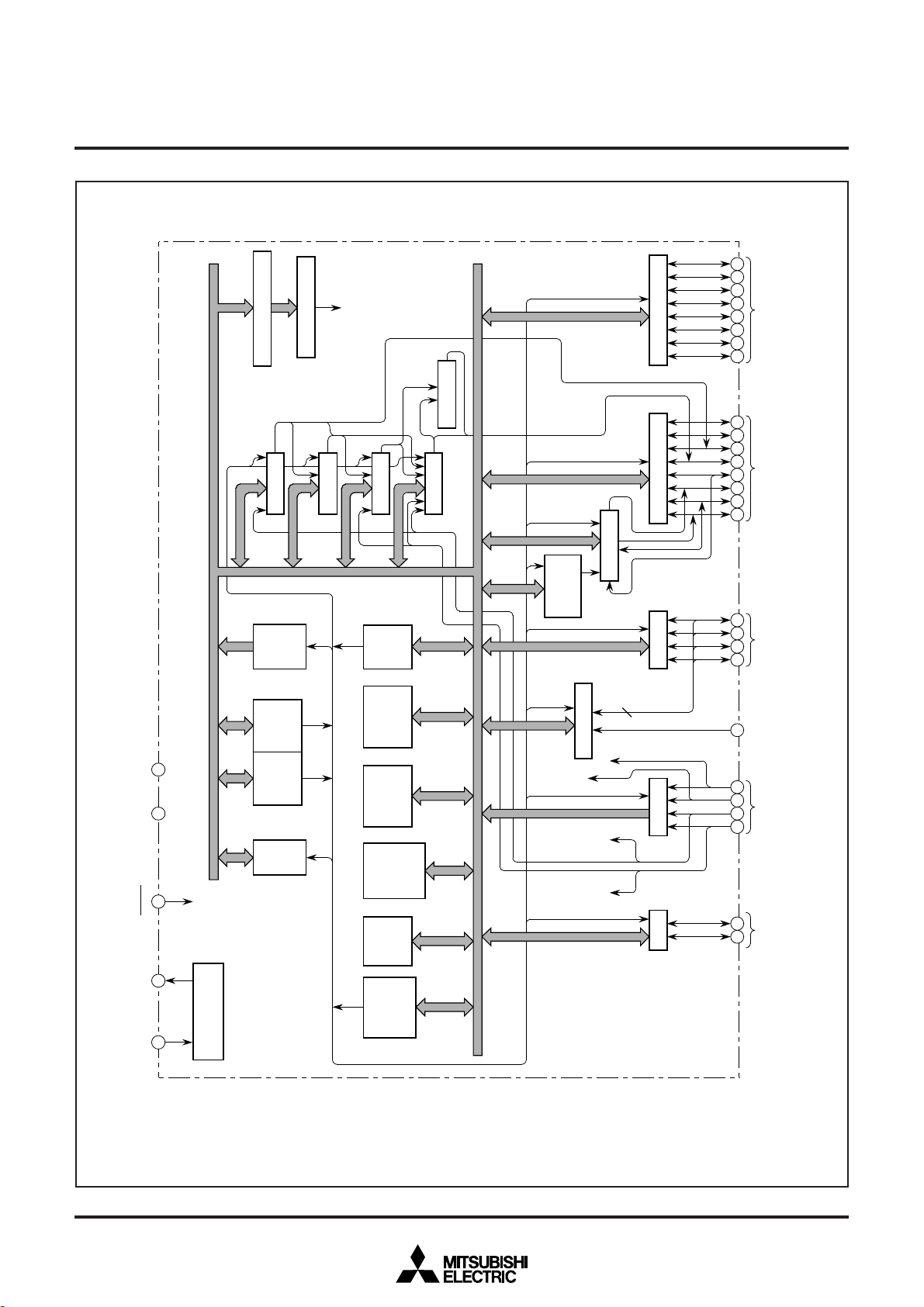
M37470M2-XXXSP BLOCK DIAGRAM
14
15
18
17
16
VCC
13
24
23
22
21
20
19
9
10
11
12
1
2
3
4
5
6
7
8
32
31
30
29
28
27
26
25
P4(2)
P3(4)
P1(8)
P0(8)
CNTR0
CNTR1
INT1
INT0
4
VSS
P2(4)
Clock generating
circuit
Clock
input
X
IN
Clock
output
X
OUT
Reset
input
RESET
ROM
4096
bytes
S I/O(8)
PWM control
A-D converter
Program
counter
PC
H(8)
Program
counter
PC
L(8)
RAM
128
bytes
Stack
pointer
S(8)
Processor
status
register
PS (8)
8-bit
Arithmetic
and logical
unit
Index
register
Y(8)
Index
register
X(8)
Accumu-
lator
A(8)
Instruction register (8)
Instruction decoder
Control signal
Timer 1 (8)
Timer 2 (8)
Timer 3 (8)
Timer 4 (8)
I/O port P4
Input port P3
V
REF
Reference
voltage input
I/O port P2
I/O port P1
I/O port P0
(Note 1)
(Note 2)
Data bus
Notes 1 : 8192 bytes for M37470M4/E4-XXXSP, and 16384 bytes for M37470M8/E8-XXXSP
2 : 192 bytes for M37470M4/E4-XXXSP, and 384 bytes for M37470M8/E8-XXXSP
Byte
counter (4)
4
7470/7471 Group
SINGLE-CHIP 8-BIT CMOS MICROCOMPUTER
MITSUBISHI MICROCOMPUTERS
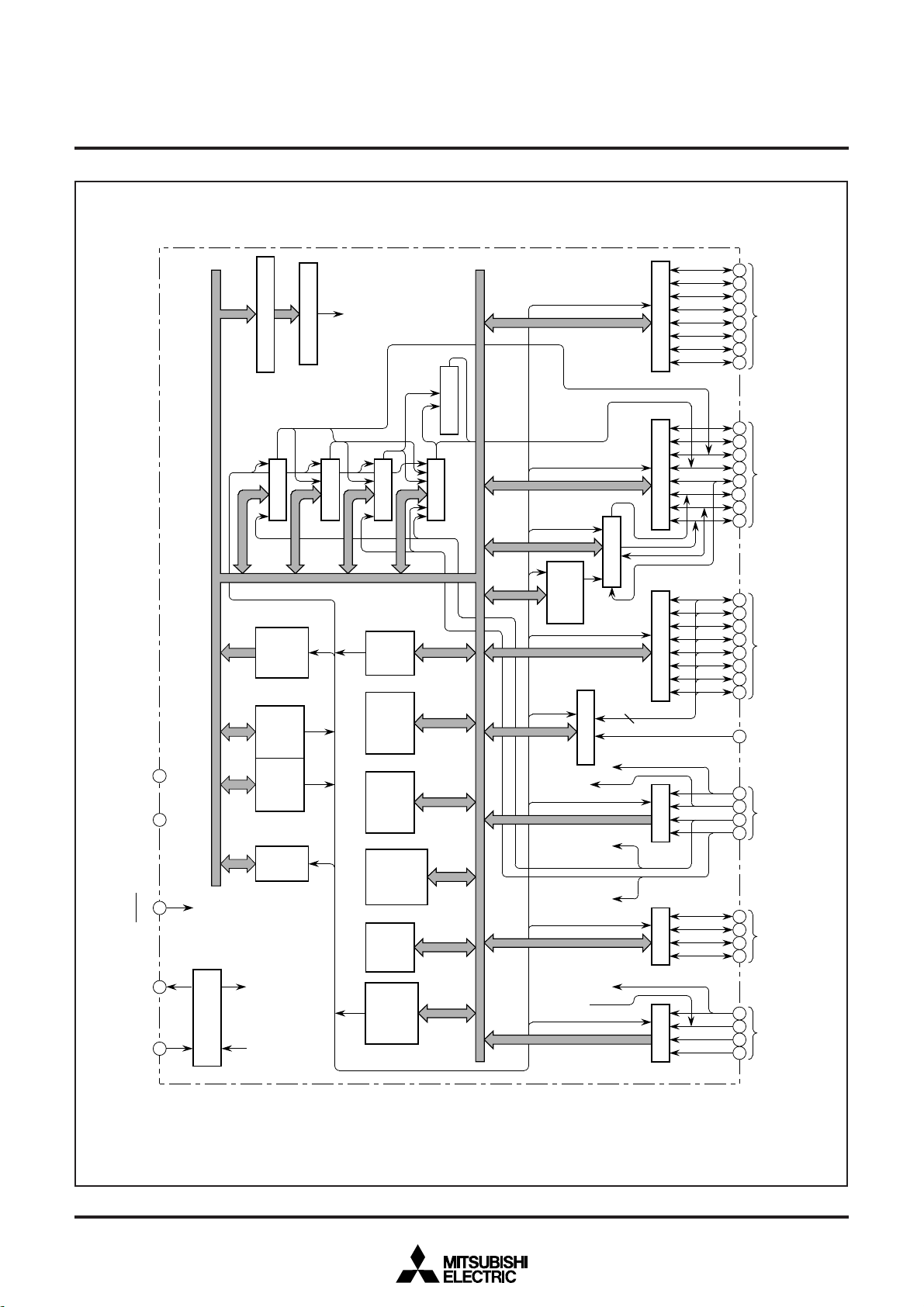
M37471M2-XXXSP BLOCK DIAGRAM
18
1
42
24
23
33
32
31
30
29
28
27
26
10
11
12
13
14
15
16
17
2
3
4
5
6
7
8
9
41
40
39
38
37
36
35
34
P5(4)
P4(4)
P3(4)
P1(8)
P0(8)
CNTR0
CNTR1
XCIN
XCOUT
INT1
INT0
8
P2(8)
19
20
XCIN
Sub-clock
input
X
COUT
Sub-clock
output
25
22
VCC
VSS
Clock generating
circuit
Main clock
input
X
IN
Main clock
output
X
OUT
Reset
input
RESET
ROM
4096
bytes
S I/O(8)
PWM control
A-D converter
Program
counter
PC
H(8)
Program
counter
PC
L(8)
RAM
128
bytes
Stack
pointer
S(8)
Processor
status
register
PS (8)
8-bit
Arithmetic
and logical
unit
Index
register
Y(8)
Index
register
X(8)
Accumu-
lator
A(8)
Instruction register (8)
Instruction decoder
Control signal
Timer 1 (8)
Timer 2 (8)
Timer 3 (8)
Timer 4 (8)
I/O port P4
Input port P3
V
REF
Reference
voltage input
I/O port P2
I/O port P1
I/O port P0
(Note 1)
(Note 2)
Notes 1 : 8192 bytes for M37471M4/E4-XXXSP, and 16384 bytes for M37471M8/E8-XXXSP, M37471E8SS
2 : 192 bytes for M37471M4/E4-XXXSP, and 384 bytes for M37471M8/E8-XXXSP, M37471E8SS
Input port P5
Data bus
Byte
counter (4)
21
5
7470/7471 Group
SINGLE-CHIP 8-BIT CMOS MICROCOMPUTER
MITSUBISHI MICROCOMPUTERS
M37471M2-XXXFP BLOCK DIAGRAM
18
19
28
23
22
V
CC
15
52
49
26
25
38
37
36
35
33
32
31
30
7
8
9
10
11
12
13
14
53
54
55
2
3
4
5
6
48
47
46
43
42
41
40
39
P5(4)
P4(4)
P3(4)
P1(8)
P0(8)
CNTR
0
CNTR
1
X
CIN
X
COUT
INT
1
INT
0
8
51
21
V
SS
AV
SS
P2(8)
Clock generating
circuit
Reset
input
RESET
ROM
4096
bytes
S I/O(8)
PWM control
A-D converter
Program
counter
PC
H
(8)
Program
counter
PC
L
(8)
RAM
128
bytes
Stack
pointer
S(8)
Processor
status
register
PS (8)
Index
register
Y(8)
Index
register
X(8)
Accumu-
lator
A(8)
Instruction register (8)
Instruction decoder
Control signal
Timer 1 (8)
Timer 2 (8)
Timer 3 (8)
Timer 4 (8)
I/O port P4
Input port P3
V
REF
Reference
voltage input
I/O port P2
I/O port P1
I/O port P0
(Note 1)
(Note 2)
Notes 1 : 8192 bytes for M37471M4/E4-XXXFP, and 16384 bytes for M37471M8/E8-XXXFP
2 : 192 bytes for M37471M4/E4-XXXFP, and 384 bytes for M37471M8/E8-XXXFP
Input port P5
Data bus
X
CIN
Sub-clock
input
X
COUT
Sub-clock
output
Main clock
input
X
IN
Main clock
output
X
OUT
Byte
counter (4)
8-bit
Arithmetic
and logical
unit
6
7470/7471 Group
SINGLE-CHIP 8-BIT CMOS MICROCOMPUTER
MITSUBISHI MICROCOMPUTERS
FUNCTIONS OF 7470/7471 GROUP
Basic machine-language instructions
Instruction execution time
Clock input oscillation frequency
Memory size
Input/Output port
Serial I/O
Timers
A-D converter
Subroutine nesting
Interrupt
Clock generating circuit
Power source voltage
Power dissipation
Input/Output characters
Operating temperature range
Device structure
Package
Input/Output voltage
Output current
M37470M2/M4/M8/E4/E8-XXXSP
M37471M2/M4/M8/E4/E8-XXXSP
M37471M2/M4/M8/E4/E8-XXXFP
M37471E8SS
Functions
71
0.5 µs (the minimum instructions, at 8 MHz oscillation frequency)
8 MHz (max.)
4096 bytes
128 bytes
8192 bytes
192 bytes
16384 bytes
384 bytes
8-bit ✕ 2
8-bit ✕ 1 (4-bit ✕ 1 for 7470 group)
4-bit ✕ 2 (Port P5 is not included in 7470 group)
4-bit ✕ 1 (2-bit ✕ 1 for 7470 group)
8-bit ✕ 1
8-bit timer ✕ 4
8-bit ✕ 1 (8 channels) (8-bit ✕ 1 (4 channels) for M37470M2/M4/M8)
64 level max. (M37470M2, M37471M2)
96
level max. (M37470M4/E4, M37471M4/E4)
192
level max. (M37470M8/E8, M37471M8/E8)
5 external interrupts, 6 internal interrupts, 1 software interrupt
Built-in circuit with internal feedback resistor (a ceramic or a quartz-
crystal oscillator)
2.7 to 4.5 V (at 2.2VCC–2.0 MHz oscillation frequency),
4.5 to 5.5 V (at 8 MHz oscillation frequency)
35 mW (at 8 MHz oscillation frequency)
5 V
–5 to 10 mA (P0, P1, P2, P4 : CMOS tri-states)
–20 to 85°C
CMOS silicon gate
32-pin shrink plastic molded DIP
42-pin shrink plastic molded DIP
56-pin plastic molded QFP
42-pin ceramic DIP
ROM
RAM
ROM
RAM
ROM
RAM
I/O
I/O
Input
I/O
Parameter
M37470M2
M37471M2
M37470M4/E4
M37471M4/E4
M37470M8/E8
M37471M8/E8
P0, P1
P2
P3, P5
P4

7
7470/7471 Group
SINGLE-CHIP 8-BIT CMOS MICROCOMPUTER
MITSUBISHI MICROCOMPUTERS
Input/
Output
PIN DESCRIPTION
Pin Name Functions
Power source voltage
Analog power
source
Reset input
Clock input
Clock output
Reference voltage
input
I/O port P0
I/O port P1
I/O port P2
Input port P3
I/O port P4
Input port P5
Input
Input
Output
Input
I/O
I/O
I/O
Input
I/O
Input
Notes 1 : AVSS for M37471M2/M4/M8/E4/E8-XXXFP.
2 : Only P2
0–P23 (IN0–IN3) 4-bit for 7470 group.
3 : Only P4
0 and P41 2-bit for 7470 group.
4 : This port is not included in 7470 group.
Apply voltage of 2.7 to 5.5 V to VCC, and 0 V to VSS.
Ground level input pin for A-D converter.
Same voltage as VSS is applied.
To enter the reset state, the reset input pin must be kept at “L” for 2 µs or more
(under normal VCC conditions).
These are I/O pins of internal clock generating circuit for main clock. To control
generating frequency, an external ceramic or a quartz-crystal oscillator is
connected between the X
IN and XOUT pins. If an external clock is used, the
clock source should be connected the XIN pin and the XOUT pin should be left
open. Feedback resistor is connected between XIN and XOUT.
Reference voltage input pin for the A-D converter.
Port P0 is an 8-bit I/O port. The output structure is CMOS output.
When this port is selected for input, pull-up transistor can be connected in
units of 1-bit and a key on wake up function is provided.
Port P1 is an 8-bit I/O port. The output structure is CMOS output.
When this port is selected for input, pull-up transistor can be connected in
units of 4-bit. P1
2, P13 are in common with timer output pins T0, T1, P14, P15,
P16, P17 are in common with serial I/O pins SIN, SOUT, CLK, SRDY, respec-
tively. The output structure of SOUT and SRDY can be changed to N-channel
open drain output.
Port P2 is an 8-bit I/O port. The output structure is CMOS output.
When this port is selected for input, pull-up transistor can be connected in
units of 4-bit.
This port is in common with analog input pins IN0–IN7.
Port P3 is a 4-bit input port. P30, P31 are in common with external interrupt
input pins INT0, INT1, and P32, P33 are in common with timer input pins
CNTR0, CNTR1.
Port P4 is a 4-bit I/O port. The output structure is CMOS output. When this
port is selected for input, pull-up transistor can be connected in units of 4-bit.
Port P5 is a 4-bit input port and pull-up transistor can be connected in units of
4-bit. P50, P51 are in common with input/output pins of clock for clock function
XCIN, XCOUT. When P50, P51 are used as XCIN, XCOUT, connect a ceramic or a
quartz-crystal oscillator between XCIN and XCOUT.
If an external clock input is used, connect the clock input to the XCIN pin and
open the XCOUT pin. Feedback resistor is connected between XCIN and XCOUT
pins.
VCC, VSS
AVSS
(Note 1)
RESET
XIN
XOUT
VREF
P00–P07
P10–P17
P20–P27
(Note 2)
P30–P33
P40–P43
(Note 3)
P50–P53
(Note 4)
8
7470/7471 Group
SINGLE-CHIP 8-BIT CMOS MICROCOMPUTER
MITSUBISHI MICROCOMPUTERS
FUNCTIONAL DESCRIPTION
Central Processing Unit (CPU)
The 7470/7471 group uses the standard 740 family instruction set.
Refer to the table of 740 family addressing modes and machine in-
structions or the SERIES 740 <Software> User’s Manual for
details on the instruction set.
Machine-resident 740 family instructions are as follows:
The FST and SLW instruction cannot be used.
The MUL, DIV, WIT, and STP instruction can be used.
CPU Mode Register
The CPU mode register is allocated at address 00FB16.
This register contains the stack page selection bit.
Fig. 1 Structure of CPU mode register
These bits must always be set to “0”.
P5
0, P51/XCIN, XCOUT selection bit (Note 2)
0 : P5
0, P51
1 : XCIN, XCOUT
XCOUT drive capacity selection bit (Note 2)
0 : Low
1 : High
Clock (XIN-XOUT) stop bit (Note 2)
0 : Oscillates
1 : Stops
Internal system clock selection bit (Note 2)
0 : X
IN-XOUT selected (normal mode)
1 : X
CIN-XCOUT selected (low-speed mode)
CPU mode register (Address 00FB16)
b7
b0
Stack page selection bit (Note 1)
0 : In page 0 area
1 : In page 1 area
1 : In the M37470M2, M37470M4/E4, M37471M2, M37471M4/E4, set this bit to “0”.
2 : In the 7470 group, set this bit to “0”.
Notes
9
7470/7471 Group
SINGLE-CHIP 8-BIT CMOS MICROCOMPUTER
MITSUBISHI MICROCOMPUTERS
MEMORY
• Special Function Register (SFR) Area
The special function register (SFR) area contains the registers
relating to functions such as I/O ports and timers.
• RAM
RAM is used for data storage as well as a stack area.
• ROM
ROM is used for storing user programs as well as the interrupt
vector area.
• Interrupt Vector Area
The interrupt vector area is for storing jump destination ad-
dresses used at reset or when an interrupt is generated.
• Zero Page
Zero page addressing mode is useful because it enables access
to this area with fewer instruction cycles.
• Special Page
Special page addressing mode is useful because it enables ac-
cess to this area with fewer instruction cycles.
Fig. 2 Memory map
RAM (192 bytes)
for
M37470M8/E8
M37471M8/E8
SFR area
Not used
Interrupt vector area
0000
16
Zero page
Special page
RAM (128 bytes)
for
M37470M2
M37471M2
ROM
(16K bytes)
for
M37470M8/E8
M37471M8/E8
ROM
(8K bytes)
for
M37470M4/E8
M37471M4/E8
ROM
(4K bytes)
for
M37470M2
M37471M2
RAM (192 bytes)
for
M37470M4/E4
M37470M8/E8
M37471M4/E4
M37471M8/E8
Not used
007F
16
00BF16
00FF16
010016
01BF16
C00016
E00016
F00016
FF0016
FFEA16
FFFF16
10
7470/7471 Group
SINGLE-CHIP 8-BIT CMOS MICROCOMPUTER
MITSUBISHI MICROCOMPUTERS
Fig. 3 SFR (Special Function Register) memory map
00C0
16
00C1
16
00C2
16
00C3
16
00C4
16
00C5
16
00C6
16
00C7
16
00C8
16
00C9
16
00CA
16
00CB
16
00CC
16
00CD
16
00CE
16
00CF
16
00D0
16
00D1
16
00D2
16
00D3
16
00D4
16
00D5
16
00D6
16
00D7
16
00D8
16
00D9
16
00DA
16
00DB
16
00DC
16
00DD
16
00DE
16
00DF
16
00E0
16
00E1
16
00E2
16
00E3
16
00E4
16
00E5
16
00E6
16
00E7
16
00E8
16
00E9
16
00EA
16
00EB
16
00EC
16
00ED
16
00EE
16
00EF
16
00F0
16
00F1
16
00F2
16
00F3
16
00F4
16
00F5
16
00F6
16
00F7
16
00F8
16
00F9
16
00FA
16
00FB
16
00FC
16
00FD
16
00FE
16
00FF
16
Port P0
Port P0 direction register
Port P1
Port P1 direction register
Port P2
Port P2 direction register
Port P3
Port P4
Port P4 direction register
Port P5 (Note 1)
Edge polarity selection register
Input latch register
A-D control register
A-D conversion register
P0 pull-up control register
P1–P5 pull-up control register (Note 2)
Timer 1
Timer 2
Timer 3
Timer 4
Timer FF register
Timer 12 mode register
Timer 34 mode register
Timer mode register 2
CPU mode register
Interrupt request register 1
Interrupt request register 2
Interrupt control register 1
Interrupt control register 2
Notes 1 : This address is not used in the 7470 group.
2 : This address is allocated P1–P4 pull-up control register for the 7470 group.
Serial I/O mode register
Serial I/O register
Serial I/O counter
Byte counter
11
7470/7471 Group
SINGLE-CHIP 8-BIT CMOS MICROCOMPUTER
MITSUBISHI MICROCOMPUTERS
INTERRUPTS
Interrupts can be caused by 12 different sources consisting of five
external, six internal, and one software sources.
Interrupts are vectored interrupts with priorities shown in Table 1.
Reset is also included in the table because its operation is similar
to an interrupt.
When an interrupt is accepted, the registers are pushed, interrupt
disable flag I is set, and the program jumps to the address speci-
fied in the vector table. The interrupt request bit is cleared
automatically. The reset and BRK instruction interrupt can never
be disabled. Other interrupts are disabled when the interrupt dis-
able flag is set.
All interrupts except the BRK instruction interrupt have an interrupt
request bit and an interrupt enable bit. The interrupt request bits
are in interrupt request registers 1 and 2 and the interrupt enable
bits are in interrupt control registers 1 and 2. External interrupts
INT
0 and INT1 can be asserted on either the falling or rising edge
as set in the edge polarity selection register. When “0” is set to this
register, the interrupt is activated on the falling edge; when “1” is
set to the register, the interrupt is activated on the rising edge.
When the device is put into power-down state by the STP instruc-
tion or the WIT instruction, if bit 5 in the edge polarity selection
register is “1”, the INT
1 interrupt becomes a key on wake up inter-
rupt. When a key on wake up interrupt is valid, an interrupt request
is generated by applying the “L” level to any pin in port P0. In this
case, the port used for interrupt must have been set for the input
mode.
If bit 5 in the edge polarity selection register is “0” when the device
is in power-down state, the INT
1 interrupt is selected. Also, if bit 5
in the edge polarity selection register is set to “1” when the device
is not in a power-down state, neither key on wake up interrupt re-
quest nor INT
1 interrupt request is generated.
The CNTR
0/CNTR1 interrupts function in the same as INT0 and
INT
1. The interrupt input pin can be specified for either CNTR0 or
CNTR
1 pin by setting bit 4 in the edge polarity selection register.
Figure 4 shows the structure of the edge polarity selection regis-
ter, interrupt request registers 1 and 2, and interrupt control
registers 1 and 2.
Interrupts other than the BRK instruction interrupt and reset are
accepted when the interrupt enable bit is “1”, interrupt request bit
is “1”, and the interrupt disable flag is “0”. The interrupt request bit
can be reset with a program, but not set. The interrupt enable bit
can be set and reset with a program.
Reset is treated as a non-maskable interrupt with the highest pri-
ority. Figure 5 shows interrupts control.
Interrupt source
RESET
INT0 interrupt
INT1 interrupt or key on wake up interrupt
CNTR0 interrupt or CNTR1 interrupt
Timer 1 interrupt
Timer 2 interrupt
Timer 3 interrupt
Timer 4 interrupt
Serial I/O interrupt
A-D conversion completion interrupt
BRK instruction interrupt
Priority
1
2
3
4
5
6
7
8
9
10
11
Vector addresses
FFFF16, FFFE16
FFFD16, FFFC16
FFFB16, FFFA16
FFF916, FFF816
FFF716, FFF616
FFF516, FFF416
FFF316, FFF216
FFF116, FFF016
FFEF16, FFEE16
FFED16, FFEC16
FFEB16, FFEA16
Remarks
Non-maskable
External interrupt (polarity programmable)
External interrupt (INT1 is polarity programmable)
External interrupt (polarity programmable)
Non-maskable software interrupt
Table 1. Interrupt vector address and priority
12
7470/7471 Group
SINGLE-CHIP 8-BIT CMOS MICROCOMPUTER
MITSUBISHI MICROCOMPUTERS
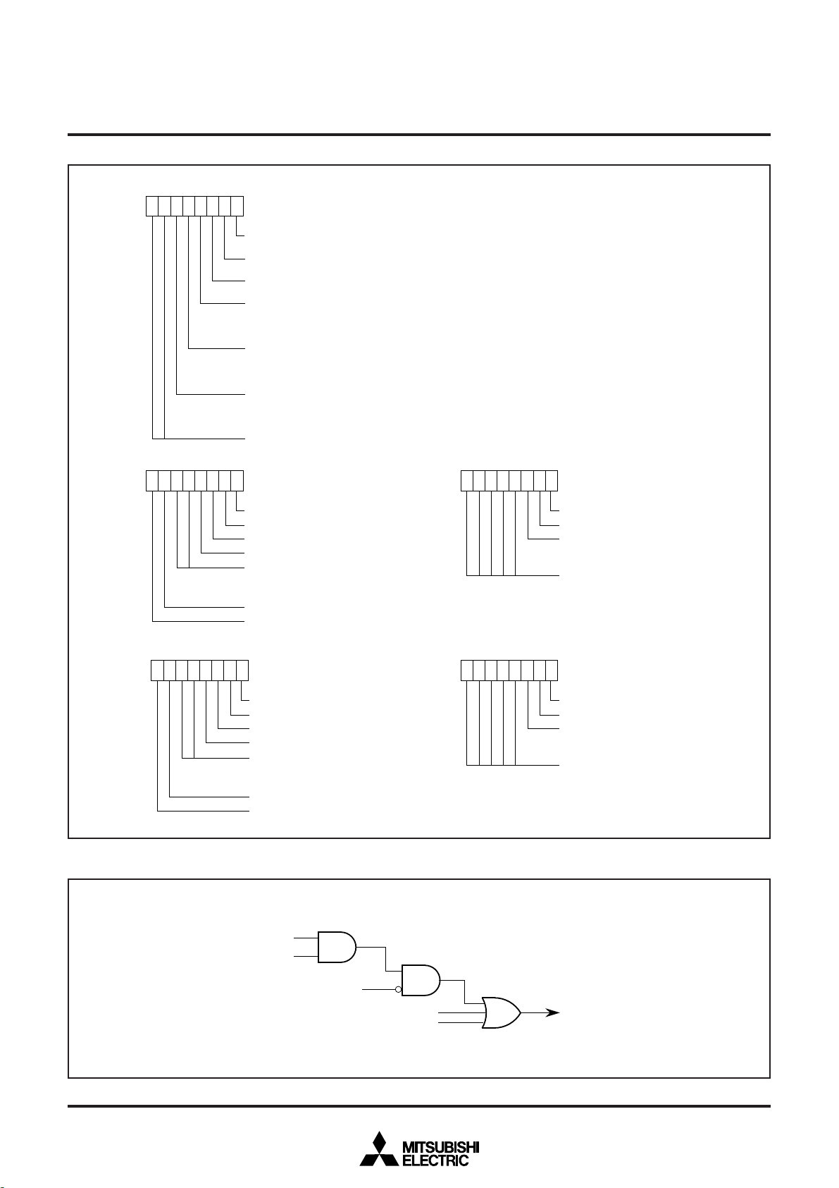
Fig. 5 Interrupt control
Fig. 4 Structure of registers related to interrupt
b7 b0
Edge polarity selection register (EG)
(Address 00D4
16
)
INT
0
edge selection bit
INT
1
edge selection bit
CNTR
0
edge selection bit
CNTR
1
edge selection bit
0 : Falling edge
1 : Rising edge
CNTR
0
/CNTR
1
interrupt selection bit
0 : CNTR
0
1 : CNTR
1
INT
1
source selection bit (at power-down state)
0 : P3
1
/INT
1
1 : P0
0
–P0
7
“L” level (for key-on wake-up)
Nothing is allocated (The value is undefined at reading)
b7 b0
Interrupt request register 1
(Address 00FC
16
)
Timer 1 interrupt request bit
Timer 2 interrupt request bit
Timer 3 interrupt request bit
Timer 4 interrupt request bit
Nothing is allocated
(The value is undefined at reading)
Serial I/O transmit interrupt request bit
A-D conversion completion interrupt request bit
b7 b0
Interrupt control register 1
(Address 00FE
16
)
Timer 1 interrupt enable bit
Timer 2 interrupt enable bit
Timer 3 interrupt enable bit
Timer 4 interrupt enable bit
Nothing is allocated
(The value is undefined at reading)
Serial I/O receive interrupt enable bit
A-D conversion completion interrupt enable bit
b7 b0
Interrupt request register 2
(Address 00FD
16
)
INT
0
interrupt request bit
INT
1
interrupt request bit
Nothing is allocated
(The value is undefined at reading)
CNTR
0
or CNTR
1
interrupt request bit
0 : No interrupt request
1 : Interrupt requested
b7
b0
Interrupt control register 2
(Address 00FF
16
)
INT
0
interrupt enable bit
INT
1
interrupt enable bit
Nothing is allocated
(The value is undefined at reading)
CNTR
0
or CNTR
1
interrupt enable bit
0 : Interrupt disable
1 : Interrupt enabled
Interrupt request bit
Interrupt enable bit
Interrupt disable flag I
BRK instruction
Reset
Interrupt request

13
7470/7471 Group
SINGLE-CHIP 8-BIT CMOS MICROCOMPUTER
MITSUBISHI MICROCOMPUTERS
TIMER
The 7470/7471 group has four timers; timer 1, timer 2, timer 3, and
timer 4.
A block diagram of timer 1 through 4 is shown in Figure 6.
Timer 1 can be operated in the timer mode, event count mode, or
pulse output mode. Timer 1 starts counting when bit 0 in the timer
12 mode register (address 00F8
16) is set to “0”.
The count source can be selected from the f(X
IN) divided by 16,
f(X
CIN) divided by 16, f(XCIN), or event input from P32/CNTR0 pin.
Do not select f(X
CIN) as the count source in the 7470 group. When
bit 1 and bit 2 in the timer 12 mode register are “0”, f(X
IN) divided
by 16 or f(X
CIN) divided by 16 is selected. Selection between f(XIN)
and f(X
CIN) is done by bit 7 in the CPU mode register (address
00FB
16). When bit 1 in the timer 12 mode register is “0” and bit 2
is “1”, f(X
CIN) is selected. And, when bit 1 in the timer 12 mode
register is “1”, an event input from the CNTR
0 pin is selected.
Event inputs are selected depending on bit 2 in the edge polarity
selection register (address 00D4
16). When this bit is “0”, the in-
verted value of CNTR
0 input is selected; when the bit is “1”,
CNTR
0 input is selected.
When bit 3 in the timer 12 mode register is set to “1”, the P1
2 pin
becomes timer output T
0. When the direction register of P12 is set
for the output mode at this time, the timer 1 overflow divided by 2
is output from T
0.
Please set the initial output value in the following procedure.
➀ Set “1” to bit 0 of the timer 12 mode register.
(Timer 1 count stop.)
➁ Set “1” to bit 0 of the timer mode register 2.
➂ Set the output value to bit 0 of the timer FF register.
➃ Set the count value to the timer 1.
➄ Set “0” to bit 0 of the timer 12 mode register.
(Timer 1 count start.)
Timer 2 can only be operated in the timer mode. Timer 2 starts
counting when bit 4 in the timer 12 mode register is set to “0”.
The count source can be selected from the divide by 16, divide by
64, divide by 128, or divide by 256 frequency of f(X
IN) or f(XCIN),
and timer 1 overflow. Do not select f(X
CIN) as the count source in
the 7470 group. When bit 5 in the timer 12 mode register is “0”,
any of the divide by 16, divide by 64, divide by 128, or divide by
256 frequency of f(X
IN) or (XCIN) is selected. The divide ratio is se-
lected according to bit 6 and bit 7 in the timer 12 mode register,
and selection between f(X
IN) and f(XCIN) is made according to bit
7 in the CPU mode register. When bit 5 in the timer 12 mode reg-
ister is “1”, timer 1 overflow is selected as the count source.
Timer 3 can be operated in the timer mode, event count mode, or
PWM mode. Timer 3 starts counting when bit 0 in the timer 34
mode register (address 00F9
16) is set to “0”.
The count source can be selected from the f(XIN) divided by 16,
f(X
CIN) divided by 16, f(XCIN), timer 1 or timer 2 overflow, or an
event input from P3
3/CNTR1 pin according to the statuses of bit 1
and bit 2 in the timer 34 mode register, bit 6 in the timer mode reg-
ister 2 (address 00FA
16) and bit 7 in the CPU mode register. Do
not select f(X
CIN) as the count source in the 7470 group. Note,
however, that if timer 1 overflow or timer 2 overflow is selected for
the count source of timer 3 when timer 1 overflow is selected for
the count source of timer 2, timer 1 overflow is always selected re-
gardless of the status of bit 6 in the timer mode register 2. Event
inputs are selected depending on bit 3 in the edge polarity selec-
tion register. When this bit is “0”, the inverted value of CNTR
1 input
is selected; when the bit is “1”, CNTR
1 input is selected.
Timer 4 can be operated in the timer mode, event count mode,
pulse output mode, pulse width measuring mode, or PWM mode.
Timer 4 starts counting when bit 3 in the timer 34 mode register is
set to “0” when bit 6 in this register is “0”. When bit 6 is “1”, the
pulse width measuring mode is selected. The count source can be
selected from timer 3 overflow, f(X
IN) divided by 16, f(XCIN) divided
by 16, f(X
CIN), timer 1 or timer 2 overflow, or an event input from
P3
3/CNTR1 pin according to the statuses of bit 4 and bit 5 in the
timer 34 mode register, bit 6 in the timer mode register 2, and bit 7
in the CPU mode register. Do not select f(X
CIN) as the count
source in the 7470 group. Note, however, that if timer 1 overflow or
timer 2 overflow is selected for the count source of timer 4 when
timer 1 overflow is selected for the count source of timer 2, timer 1
overflow is always selected regardless of the status of bit 6 in the
timer mode register 2. Event inputs are selected depending on bit
3 in the edge polarity selection register.
When this bit is “0”, the inverted value of CNTR
1 input is selected;
when the bit is “1”, CNTR
1 input is selected.
When bit 7 in the timer 34 mode register is set to “1”, the P1
3 pin
becomes timer output T
1. When the direction register of P13 is set
for the output mode at this time, the timer 4 overflow divided by 2
is output from T
1 when bit 7 in the timer mode register 2 is “0”.
Please set the initial output value in the following procedure.
➀ Set “1” to bit 3 of the timer 34 mode register.
(Timer 4 count stop.)
➁ Set “1” to bit 1 of the timer mode register 2.
➂ Set the output value to bit 1 of the timer FF register.
➃ Set the count value to the timer 4.
➄ Set “0” to bit 3 of the timer 34 mode register.
(Timer 4 count start.)
(1) Timer mode
Timer performs down count operations with the dividing ratio being
1/(n+1). Writing a value to the timer latch sets a value to the timer.
When the value to be set to the timer latch is nn
16, the value to be
set to a timer is nn
16, which is down counted at the falling edge of
the count source from nn
16 to (nn16-1) to (nn16-2) to ...0116 to
00
16 to FF16. At the falling edge of the count source immediately
after timer value has reached FF
16, value (nn16-1) obtained by
subtracting one from the timer latch value is set (reloaded) to the
timer to continue counting. At the rising edge of the count source
immediately after the timer value has reached FF
16, an overflow
occurs and an interrupt request is generated.

14
7470/7471 Group
SINGLE-CHIP 8-BIT CMOS MICROCOMPUTER
MITSUBISHI MICROCOMPUTERS
(2) Event count mode
Timer operates in the same way as in the timer mode except that
it counts input from the CNTR
0 or CNTR1 pin.
(3) Pulse output mode
In this mode, duty 50% pulses are output from the T
0 or T1 pin.
When the timer overflows, the polarity of the T
0 or T1 pin output
level is inverted.
(4) Pulse width measuring mode
The 7470/7471 group can measure the “H” or “L” width of the
CNTR
0 or CNTR1 input waveform by using the pulse width mea-
suring mode of timer 4. The pulse width measuring mode is
selected by writing “1” to bit 6 in the timer 34 mode register. In the
pulse width measuring mode, the timer counts the count source
while the CNTR
0 or CNTR1 input is “H” or “L”. Whether the CNTR0
input or CNTR1 input to be measured can be specified by the sta-
tus of bit 4 in the edge polarity selection register; whether the “H”
width or “L” width to be measured can be specified by the status of
bit 2 (CNTR
0) and bit 3 (CNTR1) in the edge polarity selection reg-
ister.
(5) PWM mode
The PWM mode can be entered for timer 3 and timer 4 by setting
bit 7 in the timer mode register 2 to “1”. In the PWM mode, the P1
3
pin is set for timer output T1 to output PWM waveforms by setting
bit 7 in the timer 34 mode register to “1”. The direction register of
P1
3 must be set for the output mode before this can be done.
In the PWM mode, timer 3 is counting and timer 4 is idle while the
PWM waveform is “L”. When timer 3 overflows, the PWM waveform
goes “H”. At this time, timer 3 stops counting simultaneously and
timer 4 starts counting. When timer 4 overflows, the PWM wave-
form goes “L”, and timer 4 stops and timer 3 starts counting again.
Consequently, the “L” duration of the PWM waveform is deter-
mined by the value of timer 3; the “H” duration of the PWM
waveform is determined by the value of timer 4.
When a value is written to the timer in operation during the PWM
mode, the value is only written to the timer latch, and not written to
the timer. In this case, if the timer overflows, a value one less the
value in the timer latch is written to the timer. When any value is
written to an idle timer, the value is written to both the timer latch
and the timer.
In this mode, do not select timer 3 overflow as the count source for
timer 4.
INPUT LATCH FUNCTION
The 7470/7471 group can latch the P30/INT0, P31/INT1, P32/
CNTR
0, and P33/CNTR1 pin level into the input latch register (ad-
dress 00D6
16) when timer 4 overflows. The polarity of each pin
latched to the input latch register can be selected by using the
edge polarity selection register. When bit 0 in the edge polarity se-
lection register is “0”, the inverted value of the P3
0/INT0 pin level is
latched; when the bit is “1”, the P3
0/INT0 pin level is latched as it
is. When bit 1 in the edge polarity selection register is “0”, the in-
verted value of the P3
1/INT1 pin level is latched; when the bit is
“1”, the P3
1/INT1 pin level is latched as it is. When bit 2 in the edge
polarity selection register is “0”, the inverted value of the P3
2/
CNTR
0 pin level is latched; when the bit is “1”, the P32/CNTR0 pin
level is latched as it is. When bit 3 in the edge polarity selection
register is “0”, the inverted value of the P3
3/CNTR1 pin level is
latched; when the bit is “1”, the P3
3/CNTR1 pin level is latched as
it is.
Loading...