


TK-285
Table of contents
 Loading...
VHF FM TRANSCEIVER
TK-285/(N)
© 2000-6 PRINTED IN JAPAN
B51-8530-00(S) 847
SERVICE MANUAL
GENERAL ................................................................................. 2
SYSTEM SET-UP ..................................................................... 2
OPERATING FEATURES......................................................... 3
REALIGNMENT ........................................................................ 4
CIRCUIT DESCRIPTION .......................................................... 6
SEMICONDUCTOR DATA ..................................................... 11
DESCRIPTION OF COMPONENTS....................................... 13
PARTS LIST............................................................................ 14
EXPLODED VIEW .................................................................. 22
PACKING ................................................................................ 23
ADJUSTMENT........................................................................ 24
TERMINAL FUNCTION .......................................................... 32
PC BOARD VIEWS
DISPLAY UNIT (X54-3210-13) ............................................ 33
TX-RX UNIT (X57-619X-XX) ............................................... 39
SCHEMATIC DIAGRAM ......................................................... 45
BLOCK DIAGRAM .................................................................. 49
LEVEL DIAGRAM ................................................................... 51
OPTIONS ................................................................................ 52
SPECIFICATIONS ...............................................BACK COVER
CONTENTS
CAUTION
When using an external power connector, please use
with maximum final module protection of 9V.
Photo is K type
Knob (ENC)
(K29-5232-03)
Knob (VOL)
(K29-5231-03)
Cabinet assy
(A02-2055-53)
(16 keys)
Badge
(B43-1106-14)
Packing
(G53-0896-02)
(16 keys)
Panel assy
(A62-0535-04)
Helical antenna
(T90-0733-05):K, E
(T90-0734-05):(N)M
Knob (PTT etc)
(K29-5157-03)

TK-285/(N)
2
GENERAL / SYSTEM SET-UP
Unit
Model &
TX-RX unit Display unit Frequency range Remarks Charger Battery
destination
K
X57-6190-11
RX : 217~250MHz
IF1 : 44.85MHz
OP
TK-285
E
X54-3210-13 TX : 218~250MHz
LOC : 44.395MHz
OP ✔
(N)M X57-6190-21 240~270MHz
Merchandise received
Choose the type of transceiver
Transceiver programming
Delivery
Are you using the speaker microphone?
TX 218~250
RX 217~250
5.0W TK-285 K,E
TX/RX 240~270 5.0W TK-285 (N)M
Frequency range (MHz) RF power Type
A personal computer (IBM PC or compatible), programming
interface (KPG-36), and programming software (KPG-62D)
are required for programming.
(The frequency, conventional system features, TX power HI/LOW,
and signalling data are programmed for the transceiver.)
YES
NO
KMC-25
Speaker microphone
(Option)
SYSTEM SET-UP
INTRODUCTION
SCOPE OF THIS MANUAL
This manual is intended for use by experienced technicians
familiar with similar types of commercial grade communications
equipment. It contains all required service information for the
equipment and is current as of the publication data. Changes
which may occur after publication are covered by either Service
Bulletins or Manual Revisions. These are issued as required.
ORDERING REPLACEMENT PARTS
When ordering replacement parts or equipment information,
the full part identification number should be included. This
applies to all parts : components, kits, or chassis. If the part
number is not known, include the chassis or kit number of which
it is a part, and a sufficient description of the required
component for proper identification.
PERSONNEL SAFETY
The following precautions are recommended for personnel
safety:
●
DO NOT transmit until all RF connectors are verified secure
and any open connectors are properly terminated.
●
SHUT OFF and DO NOT operate this equipment near
electrical blasting caps or in an explosive atmosphere.
●
This equipment should be serviced by a qualified technician
only.
SERVICE
This radio is designed for easy servicing. Refer to the
schematic diagrams, printed circuit board views, and alignment
procedures contained within.
OP

TK-285/(N)
3
OPERATING FEATURES
1. Operation Features
The TK-285 is a VHF FM Radio designed in both Trunking
Mode and Conventional Mode.
2. Transceiver Controls and Indicators
2-1. Physical Layout
2-2. Panel controls
The key on the top and front panel is momentary-type push
buttons. The functions of these keys and knob are explained
below.
1 Antenna connector
Connect the antenna here.
2 Rotary encoder
3 POWER switch/ VOLUME control
Turn clockwise to switch ON the transceiver. Rotate to
adjust the volume. Turn conterclockwise fully to switch OFF
the transceiver.
4 Auxiliary (orange) key
5 Battery pack release latch
Pull back on this latch to release the battery pack.
6 Call key
7 PTT (Push-To-Talk) switch
8 Clear key
9 Transmit/ Receive indicator
0 A key
- B key
= 2 C key
~ D 3 key
! DTMF keypad
@ Universal connector
Connect the (optional KMC-25) speaker/ microphone here.
Otherwise, keep the supplied cover in place.
2-3. Key functions
Trunking mode
2 Rotary encoder
Rotate this encoder to select your desired call address
(voice calls) ot status (status calls).
4 Auxiliary (orange) key (default setting: None)
Press to activate its auxiliary function.
6 Call key
Press to call the displayed call address.
7 PTT (Push-To-Talk) switch
Press to transmit. Also press to initiate a call if “PTT to
Initiate Call” has been programmed.
8 Clear key
Press to end the current call.
9 Transmit indicator
Lights red while transmitting.
0 A key (default setting: Status/ Stack)
Press to activate its auxiliary function.
- B key (default setting: Redial)
Press to activate its auxiliary function.
= 2 C key (default setting: None)
Press to activate its auxiliary function. Also press to scroll
left while viewing stack entries.
~ D 3 key (default setting: None)
Press to activate its auxiliary function. Also press to scroll
right while viewing stack entries.
! DTMF keypad
Press to input a call address or dialing function.
Conventional mode
2 Rotary encoder
Rotate this encoder to select your desired channel.
6 Call key
Press to turn the monitor function ON in order to monitor
your selected channel.
7 PTT (Push-To-Talk) switch
Press this switch, then speak into the microphone to call a
station.
8 Clear key
Press to return to Trunking mode.
9 Transmit/ Receive indicator
Lights green while receiving a signal. Lights red while
transmitting.
0 A key
Press to turn Scan ON (or OFF).
- B key
Press to add/delete channel(s) to/from Scan list.
~ D 3 key
Press to turn the display and keypad backlight ON.
The backlight remains ON for 5 seconds.
eqw
r
t
o
!5
!0
!4
i
u
y
!1
!2
!3
SpeakerMicrophone

TK-285/(N)
4
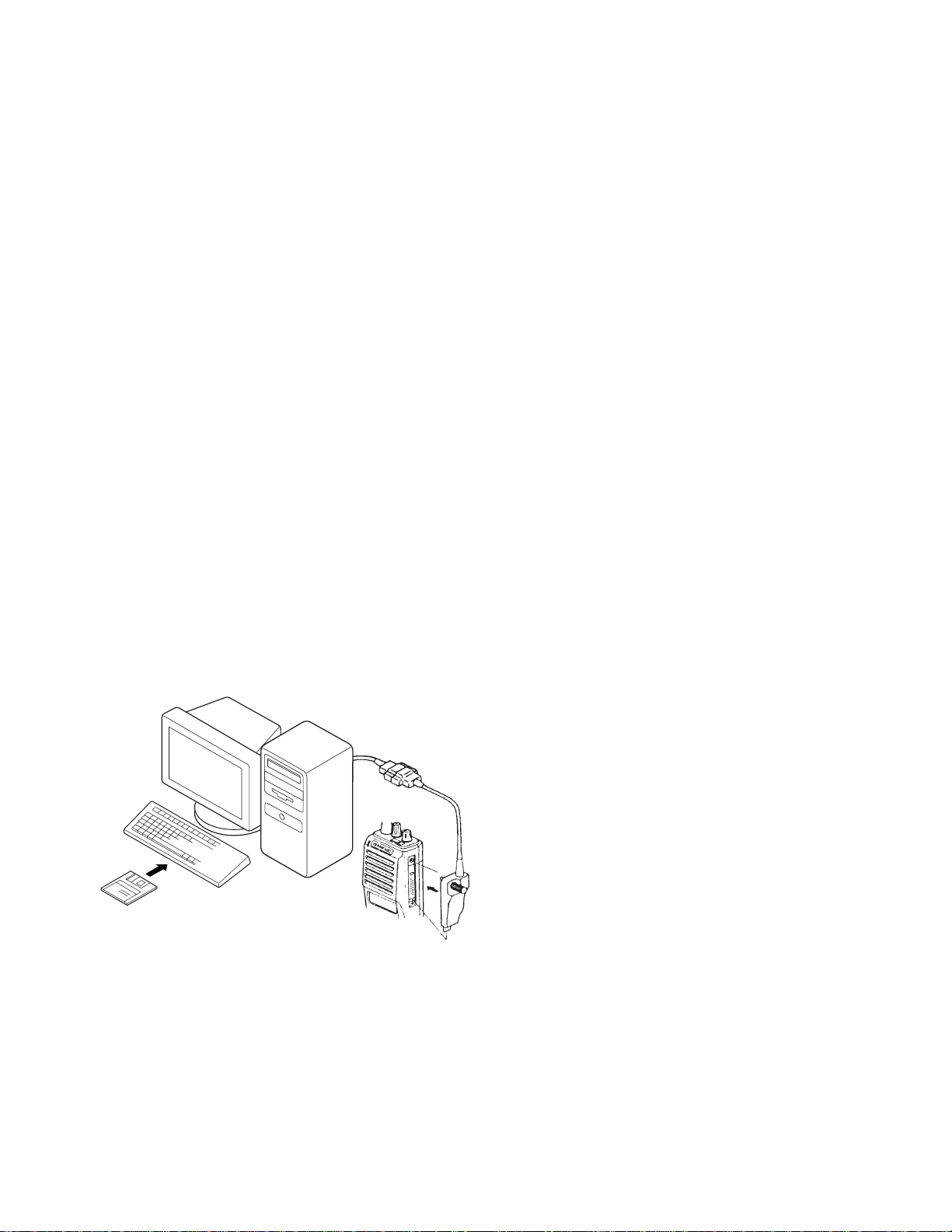
5. PC Mode
5-1. Preface
The TK-285 transceiver is programmed by using a personal
computer, programming interface (KPG-36) and programming
software (KPG-62D).
The programming software can be used with an IBM PC or
compatible. Figure 1 shows the setup of an IBM PC for
programming.
5-2. Connection procedure
1. Connect the TK-285 to the personal computer with the
interface cable.
2. When the POWER switch on, user mode can be entered
immediately. When PC sends command the radio enter PC
mode, and “PROGRAM” is displayed on the LCD.
When data transmitting from transceiver, the red LED is
blinking.
When data receiving to transceiver, the green LED is blinking.
Notes:
• The data stored in the personal computer must match model
type, when it is written into the flash memory.
• Change the TK-285 to PC mode, then attach the interface
cable.
REALIGNMENT
1. Modes
Mode Function
User mode For normal use.
Panel test mode Used by the dealer to check the
fundamental characteristics.
Panel tuning mode Used by the dealer to tune the radio.
PC mode Used for communication between the
radio and PC (IBM compatible).
Data program- Used to read and write frequency data
ming mode
and other features to and from the radio.
PC test mode Used to check the radio using the PC.
This feature is included in the FPU.
See panel tuning.
Firmware program- Used when changing the main
ming mode program of the flash memory.
User mode
Panel test mode
PC mode
Firmware
programming mode
Panel tuning mode
PC test mode
Data programming
mode
PC tuning mode
3. Panel Test Mode
Setting method refer to ADJUSTMENT.
4. Panel Tuning Mode
Setting method refer to ADJUSTMENT.
2. How to Enter Each Mode
Mode Operation
User mode Power ON
Panel test mode [B]+Power ON
PC mode Received commands from PC
Panel tuning mode [Panel test mode]+[A]
Firmware programming mode
[A]+Power ON
OPERATING FEATURES / REALIGNMENT
2-4. Display
1 Sub display
displays the strength of received signals.
2 Programming indicator
P appears while in AUX A or Scrambler is being activated.
3 MON (Monitor) indicator
MON appears while you are monitoring a channel by pressing
the Call key. (Conventional Mode only)
4 SVC (Service) indicator
SVC appears when a control channel is found. It flashes
while the transceiver is searching for a control channel.
5 SCN (Scan) indicator
SCN appears while you are scanning. (Conventional Mode
only)
6 LO indicator
This icon blinks while in battery warning, if “Always” or
“Always W/beep” is selected in the battery warning settings.
7 Handset indicator
flashes when you activate call diversion.
8 MAIL indicator
appears while there is data in the stack. It flashes when
there is new data in the stack.
9 Alphanumeric display
displays call addresses, the call
duration timer, data messages, and the current operating
status of the transceiver.
SVC
MON
SCN LO
12345
9
678
TK-285/(N)
5
REALIGNMENT
5-3. KPG-36 description
(PC programming interface cable: Option)
The KPG-36 is required to interface the TK-285 to the
computer. It has a circuit in its D-subconnector (25-pin) case
that converts the RS-232C logic level to the TTL level.
The KPG-36 connects the universal connector of the TK-
285 to the computers RS-232C serial port.
5-4. Programming software KPG-62D Description
The KPG-62D is the programming software for the
transceiver supplied on three 3.5" floppy disks. This software
runs under MS-Windows 95/98 on an IBM-PC or compatible
machine.
The data can be input to or read from the trnsceiver and
edited on the screen. The programmed or edited data can be
printed out. It is also possible to tune the transceiver.
We recommend that install the KPG-62D for example to
hard disk first then use it.
5-5. Programming with IBM PC
If data is transferred to the transceiver from an IBM PC with
the KPG-62D, the destination data (basic radio information)
for each set can be modified. Normally, it is not necessary to
modify the destination data because their values are
determined automatically when the frequency range (frequency
type) is set.
The values should be modified only if necessary. Data can
be programmed into the flash memory in RS-232C format via
the universal connector.
KPG-62D instruction manual parts No. : B62-1354-XX
6-3. Programming
1. Start up the firmware programming software (Fpro.exe).
2. Set the communications speed (normally, 57600 bps) and
communications port in the configuration item.
3. Set the firmware to be updated by File name item.
4. Turn the TK-285 power ON with the [A] switch held down.
Hold the switch down until the display changes to "PROG
57600". When "PROG 57600" appears, release your finger
from the switch.
5.
Check the connection between the TK-285 and the personal
computer, and make sure that the TK-285 Is in the Program mode.
6. Press write button in the window. A window opens on the
display to indicate progress of writing. When the TK-285
starts to receive data. the [P] icon is blinking.
7. If writing ends successfully. the LED on the TK-285 lights
and the checksum is displayed.
8. If you want to continue programming other TK-285 s, repeat
steps 4 to 7.
Notes:
●
This mode cannot be entered if the Firmware Programming
mode is set to Disable in the Programming software (KPG-
62D).
●
When programming the firmware, it is recommend to copy
the data from the floppy disk to your hard disk before update
the radio firmware.
Directry copying from the floppy disk to the radio may not
work because the access speed is too slow.
6-4. Function
1. If you press the [Call] switch (top of left side) while "PROG
57600" is displayed, the version is displayed. If you press
the [Call] switch again while the version is displayed, "PROG
57600" is redisplayed.
2. If you press the [Clear] switch (bottom of left side) while
"PROG 57600" is displayed, the display changes to "PROG
19200" to indicate that the write speed is low speed (19200
bps). If you press the [Clear] switch again while "PROG
19200" is displayed, the display changes to "PROG 38400",
and the write speed becomes the middle-speed mode
(38400 bps). If you press the [Clear] switch again while
"PROG 38400" is displayed, the display returns to "PROG
57600".
3. If you press the [Clear] switch while the version is displayed,
the checksum is displayed. If you press the [Clear] switch
again while the checksum is displayed, the version is
redisplayed.
Note:
Normally, write in the high-speed mode.
KPG-36
IBM-PC
KPG-62D
Fig. 1
6. Firmware Programming Mode
6-1. Preface
Flash memory is mounted on the TK-285. This allows the
TK-285 to be upgraded when new features are released in the
future. (For details on how to obtain the firmware, contact
Customer Service.)
6-2. Connection procedure
Connect the TK-285 to the personal computer (IBM PC or
compatible) with the interface cable (KPG-36). (Connection is
the same as in the PC Mode.)

TK-285/(N)
6
Fig. 2 Receiver section
IC12
MIX, DET, IF
SW
Q15
DMDM
IC4 (2/2)
AF AMP
5
DE-
EMP
MUTE
EXP
HPF LPF HPF BEF
IC13
21
VOL
IC8
IC7 (2/2)
AF AMP
41
VC1
VC2
Q310
SSW
INT.
SP
EXT.
SP
2nd local
OSC
X2
AF
AF
SW
IC300
AF PA
ANT
SW
L40,42,
43
L403,404,
405,406
BPF
D12,14,
D15,401
Q24
RF
AMP
ANT
IC18
1st MIX
Q12
1st IF
L27,29
BEF
L31,33
BPF
XF1
MCF
1st Local
OSC (PLL)
CF2
1. Overview
This transceiver is VHF/FM portable transceiver designed
to operate in the frequency range of 217 to 250MHz (K, E),
240 to 270MHz ((N)M).
2. Circuit Configuration by Frequency
The receiver is a double-conversion superheterodyne with
a first intermediate frequency (IF) of 44.85MHz and a second
IF of 455kHz. Incoming signals from the antenna are mixed
with the local signal from the PLL to produce the first IF of
44.85MHz.
This is then mixed with the 44.395MHz second local
oscillator output to produce the 455kHz second IF. This is
detected to give the demodulated signal.
The transmit signal frequency is generated by the PLL VCO,
and modulated by the signal from the microphone. It is then
amplified and sent to the antenna.
ANT
RX : 217~250MHz (K,E)
RX : 240~270MHz ((N)M)
TX : 218~250MHz (K,E)
TX : 240~270MHz ((N)M)
ANT
SW
RF
AMP
PA
AMP
TX
AMP
1st MIX
MCF
44.85MHz
CF
455kHz
FM IF
SYSTEM
AF
AMP
SP
44.395MHz
261.85~294.85MHz (K,E)
284.85~314.85MHz ((N)M)
PLL
VCO
MIC
AMP
MIC
218~250MHz (
K,E
)
240~270MHz (
(N)M
)
Fig. 1 Frequency configuration
3. Receiver System
3-1. RF unit
An incoming RF signal from the antenna terminal is passed
through the antenna switch (D12, D14, D22 and D401 are off)
and then the bandpass filter (L403,404,405,406). The bandpass
filter is adjusted by a variable capacitor. The input voltage to
the variable capacitor is regulated by the voltage output from
the D/A converter (IC8). The signal is amplified by RF amplifier
(Q24), and passed through the bandpass filter (L31,33) and
band-eliminate filter (L27,29) to remove the spurious signal
again. The resulting signal is applied to the first mixer (IC18),
where it is mixed with the first local oscillator signal output
from the frequency synthesizer to produce the first IF
(44.85MHz). The 1st mixer uses the GaAs IC.
3-2. IF unit
The first IF signal is passed through a crystal filter (XF1) to
remove a adjacent channel signal. The filtered first IF signal is
amplified by the first IF amplifier (Q12) and then applied to the
lF system IC (IC12). The IF system IC provides a second mixer,
second local oscillator, limiting amplifier, quadrature detector
and RSSI (Received Signal Strength Indicator). The second
mixer mixes the first IF signal with the 44.395MHz of second
local oscillator output (crystal unit X2) and produces the second
IF signal of 455kHz.
The second IF signal is passed through the ceramic filter
(CF2) to more remove the adjacent channel signal. The filtered
second IF signal is amplified by the limiting amplifier and
demodulated by the quadrature detector with ceramic
discriminator (CD1). The demodulated signal is routed to the
audio circuit.
CIRCUIT DESCRIPTION

TK-285/(N)
7
CIRCUIT DESCRIPTION
3-3. Audio amplifier circuit
The demodulated signal from IC12 goes through the mute
switch (Q15) and is amplified by IC4 (2/2), high-pass filtered,
low-pass filtered, high-pass filtered, band-eliminate filtered, and
de-emphasized by IC13.
The signal then goes through an AF amplifier IC7 (2/2), an
electronic volume control (IC8), and an AF switch (Q310 is
on), and is routed to audio power amplifier (IC300), where it is
amplified and output to the internal speaker.
The audio mute signal (AM) from the shift register becomes
Low in the standby and Q304, Q305 which are power supply
circuit for IC300 turn off. Also, IC13 is set to the power down
mode according to data from microprocessor, and the AF signal
is muted. When the audio is output, AM becomes High to turn
Q304, Q305 ON, and voltage is supplied to power terminal VP
of IC300. Also, IC13 is canceled out of the power down mode.
The speaker is switched by the logic of speaker switching
terminal SSW on the universal connector. When SP-MIC is
not attached, the logic of SSW becomes High and SW (Q310)
is turned ON, and the AF signal is input to both amplifiers of
IC300.
When SP-MIC is attached, SSW is connected to GND at
inside of SP-MIC. For this reason, Q310 is turned OFF, and
the AF signal is input only to amplifier for EXT SP of IC300.
Change of INT/EXT SP refer to Fig. 3.
AM SSW VC1 VC2 SP
H H H L INT
H L L H EXT
L H L L MUTE
L L L L MUTE
Fig. 3 Audio amplifier circuit
SW
IC300
2
8
AM
AF
SSW
INT.SP
EXT.SP
Q305
Q304
SB
VP 5
VC1
VC2
Q308
Q301
Fig. 5 Squelch and RSSI voltage vs ANT input level
Fig. 4 Squelch circuit
12
DET
BPF
AMP
DET
RSSI
NOISE
AMP
IC19
CPU
IF AMP
7
91
93
IC12 : FM IF IC
Q4 D4
SQ close
SQ open
Preset Value
ANT input level
SQ voltage
ANT input level
T
T
T
T
T
RSSI voltage
S-Meter level
3-4. Squelch circuit
The output from IC12 enters FM IC again, then passed
through a band-pass filter. The noise component output from
IC12 is amplified by Q4 and rectified by D4 to produce a DC
voltage corresponding to the noise level. The DC voltage is
sent to the analog port of the CPU (IC19). And IC12 outputs a
DC voltage (RSSI) corresponding to the input of the IF amplifier.
The CPU reads the RSSI signal via pin 93.
IC19 determines whether to output sounds from the speaker
by comparing the input voltage of pin 91 and pin 93 with the
preset value.
4. Transmitter System
4-1. Microphone amplifier
The signal from the internal microphone goes through the
mute switch (Q300).
When the SP-MIC is not attached, the microphone switching
terminal (MSW) on the universal connector becomes High, and
mute switch (Q300) is turned ON. When the SP-MIC is
attached, MSW is connected to GND at inside of SP-MIC. For
this reason, Q300 is turned OFF, the internal microphone is
muted, and only the input of the external microphone is supplied
to the microphone amplifier of the TX-RX unit.
The signal from microphone passes through the limitter
circuit in D8, and Mic mute switch (Q17 is off in TX) and through
the low-pass filter (IC25:1/2), the high-pass filter, the ALC
circuit, the low-pass filter, the high-pass filter, and pre-
emphasis/IDC circuit in IC13. When encoding DTMF, mute
switch (Q13) is turned OFF for muting the microphone input
signal.
The signal passes through the D/A converter (IC8) for the
maximum deviation adjustment, and enters the summing
amplifier consisting of IC7 (1/2), and is mixed with the low speed
data from the CPU (IC19) and 9600bps DATA from Optional
Board Terminal.

TK-285/(N)
8
Fig. 8 PLL block diagram
T/R
(TX : Low)
T/R
A1
VCO
CV
5
IC14
PLL
8
BUFF
BUFF
LPF
DT,CP,EP
CPU
UL
IC19
VCXO
IC1
FC
BAL
Q18
SW
D9
To
drive
amp
Q16
X1
To mixer
SW
MB
D23
18
5. Frequency Synthesizer Unit
5-1. Frequency synthesizer
The frequency synthesizer consists of the VCXO (X1), VCO
(A1), PLL IC(IC14) and buffer amplifiers.
The VCXO generates 16.8MHz. The frequency stability is
1.5ppm within the temperature range of -30 to +60˚C. The
frequency tuning and modulation of the VCXO are done to
apply a voltage to pin 1 of the VCXO. The output of the VCXO
is applied to pin 8 of the PLL IC.
The TK-285’s VCO consists of 2VCO and covers a dual
range of the 261.85~294.85MHz (K,E), 284.85~314.85MHz
((N)M) and the 218~250MHz (K,E), 240~270MHz ((N)M).
The VCO generates 261.85~294.85MHz (K,E),
284.85~314.85MHz ((N)M) for providing to the first local signal
in receive. In TX, the pin 3 of the VCO goes low and the VCO
generates 218~250MHz (K,E), 240~270MHz ((N)M).
The output of the VCO is amplified by the buffer amplifier
(Q16) and routed to the pin 5 of the PLL IC. Also the output of
the VCO is amplified by the buffer amplifier (Q18) and routed
to the next stage according to T/R switch (D9, D23).
The PLL IC consists of a prescaler, fractional divider,
reference divider, phase comparator, charge pump. This PLL
IC is fractional-N type synthesizer and performs in the 40, 50
or 60kHz reference signal which is eighth of the channel step
(6.25kHz). The input signal from the pins 5 and 8 of the PLL IC
is divided down to the 50kHz and compared at phase
comparator. The pulsed output signal of the phase comparator
is applied to the charge pump and transformed into DC signal
in the loop filter (LPF). The DC signal is applied to the pin 1 of
the VCO and locked to keep the VCO frequency constant.
PLL data is output from DT (pin 75). CP (pin 19) and EP
(pin 47) of the microprocessor (IC19). The data are input to
the PLL IC when the channel is changed or when transmission
is changed to reception and vice versa.
CIRCUIT DESCRIPTION
Fig. 6 Microphone amplifier
12
HPF
LPF HPF IDC
PRE
EMP
ALC
COMP
SW
LIMIT
SW
MIC
Q300 D8
LPF
IC25(1/2)
MIC
EXT.
MIC
Q301
IC13
15
16
18 19
Q13
MUTE
DTMF
98
6
D/A
D/A
IC8
IC8 IC1
I5
O5
I1
O1
D/A
IC8
I2
O2
LSD DI9
IC7 (1/2)
SUM
AMP
BUFF
AMP
VCXO
VCO
A1
X1
MIC
MUTE
Q17
PTTMSW
The output signal from the summing amplifier passes
through the D/A converter (IC8) again and goes to the VCO
modulation input.
The other output signal from the summing amplifier passes
through the D/A converter (IC8) again for the BAL adjustment,
and the buffer amplifier (IC1 : 2/2), and goes to the VCXO
modulation input.
Fig. 7 Drive and final amplifier and APC circuit
From
T/R SW
(D9)
DRIVE
AMP
RF
POWER AMP
LPF
ANT
SW
D12,D401
ANT
VGG
Q20 IC100
VDD
R244
R246
R248
+B
IC23
(1/2)
IC23
(2/2)
REF
VOL
(IC8)
4-2. Drive and Final amplifier
The signal from the T/R switch (D9 is on) is amplified by
drive amplifier (Q20) to 30mW.
The output of the drive amplifier is amplified by the RF power
amplifier (IC100) to 5.0W (1W when the power is low). The RF
power amplifier consists of two stages MOS FET transistor.
The output of the RF power amplifier is then passed through
the harmonic filter (LPF) and antenna switch (D12 and D401
is on) and applied to the antenna terminal.
4-3. APC circuit
The APC circuit always monitors the current flowing through
the RF power amplifier (IC100) and keeps a constant current.
The voltage drop at R244, R246 and R248 is caused by the
current flowing through the RF power amplifier and this voltage
is applied to the differential amplifier (IC23 1/2).
IC23(2/2) compares the output voltage of IC23(1/2) with the
reference voltage from IC8, and the output of IC23(2/2) controls
the VGG of the RF power amplifier to make the both voltages
to same voltage.
The change of power high/low is carried out by the change
of the reference voltage. Q22,23 and 25 are turned on in
transmit and the APC circuit is active.

TK-285/(N)
9
CIRCUIT DESCRIPTION
IC19
IC17
CPU
IC20
EEPROM
FLASH
6-2. Low battery warning
The battery voltage is monitored by the microprocessor
(IC19). When the battery voltage falls below the voltage set by
the Low Battery Warning adjustment, the red LED flashes to
notify the operator that it is time to replace the battery. If the
battery voltage falls even more (approx. 5.8V), a beep sounds
and transmission is stopped.
6. Control Circuit
The control circuit consists of microprocessor (IC19) and
its peripheral circuits. It controls the TX-RX unit and transfers
data to and from the display unit. IC19 mainly performs the
following;
1) Switching between transmission and reception by PTT
signal input.
2) Reading system, group, frequency, and program data
from the memory circuit.
3) Sending frequency program data to the PLL.
4) Controlling squelch on/off by the DC voltage from the
squelch circuit.
5) Controlling the audio mute circuit by decode data input.
6) Transmitting tone and encode data.
6-1. Memory circuit
Memory circuit consists of the CPU (IC19) and a flash
memory (IC17).
A flash memory has a capacity of 2M bits and contains the
transceiver control program for the CPU and the data for
operating features.
This program can be easily downloaded from an external
device.
●
Flash Memory
Note : The flash memory stores the data containing the FPU
(KPG-62D) program, Security Number (MPT Serial Number)
and firmware program (User mode, Test mode, Tuning mode,
etc.).
This data must be reinstalled when replacing the flash memory.
●
EEPROM
Note : The EEPROM stores tuning data (Deviation, Squelch,
etc.)
Realign the transceiver after replacing the EEPROM.
Low battery warning
The red LED flashes during
transmission
The red LED flashes and
continuous beep sounds
while PTT pressed
Battery condition
The battery voltage is low but
the transceiver is still usable.
The battery voltage is low and
the transceiver is not usable
to make calls.
6-3. Key input
If the clock is supplied to CLK terminal when the RES
terminal (CPU pin 78) of the decade counter (IC301) is set to
Low, Q0 to Q7 become High sequentially. Normally, KI1 and
KI2 are Low (pulled down). When any key is pressed. KI1 or
KI2 become High. The CPU detects which key is pressed,
according to the voltage of KI1 and Kl2 and clock timing.
Fig. 10 Key input
IC19
CPU
Q5
Q1
Q0
Q2
Q6
Q7
Q3
Vss
Vdd
RES
CLK
CL
CA
Q9
Q4
Q8
KI1
KI2
CK
KRST
IC301
16 keys
RESET
CLOCK
Q0
Q1
Q2
Q3
Q4
Q5
Q6
Q7
Q8
Q9
CLOCK
INHIBIT
CARRY
OUT
Fig. 11 Decade counter timing chart
Fig. 9 Memory circuit

TK-285/(N)
10
8. Power Supply Circuit
Battery +B is supplied via a 3A fuse from the battery terminal
connected to the TX-RX unit. After passing through the power
switch, power supply (SB) is applied to the three AVRs. IC5
supplies 5V (5M) to the control circuit, and IC9 supplies 5V
(5C) to common circuits. IC6 supplies to the TX circuit, the RX
circuit and common circuits of needless save mode. During
transmission, 5TC becomes Low and Q3 is turned ON to supply
5V (5T) to the TX circuit. During reception, 5RC becomes Low
and Q2 is turned ON to supply 5V (5R) to the RX Circuit.
Fig. 14 Power supply circuit
Fig. 13 Decode
IC4
AMP
IC13
AF IC
IC11
LPF
IC19
CPU
AF
RDT
LSD
IN
21
95
CIRCUIT DESCRIPTION
Fig. 12 Encode
SUM
SUM
IC7(1/2)
SUM
R166
R162
C176
C170
R136
1
LSD
OUT
HSD
OUT
IC19
CPU
O5
O2
O3
O6
I2
I1
I5
IC8
D/A (ADJ)
VCO
MD
A1
RX Audio
MIC IN
IC13
2
LPF
IC10
I6
I3
VCXO
X1
MB
AF
AMP
IC7 (2/2)
O1
BUFF
AMP
IC1
7-2. Decode
●
Low-speed data (QT,DQT)
The demodulated signal from the IF IC (IC12) is amplified
by IC4 (2/2) and passes through a low-pass filter (IC11) to
remove audio components. The signal is input to pin 95 of the
CPU.
The CPU digitizes this signal, performs processing such as
DC restoration, and decodes the signal.
●
FFSK
The FFSK input signal from the IF IC is amplified by IC4
(1/ 2) and goes to pin 5 of IC13. The signal is demodulated by
FFSK demodulator in IC13. The demodulated data goes to
the CPU for processing.
7. Signalling Circuit
7-1. Encode
●
Low-speed data (QT,DQT)
Low-speed data is output from pin 1 of the CPU. The signal
passes through a low-pass CR filter, and goes to the summing
amplifier (IC7 1/2). The signal is mixed with the audio signal
and goes to the VCO (A1) and VCXO (X1) modulation input
after passing through the D/A converter (IC8) for BAL
adjustment.
●
High-speed data (DTMF)
High-speed data (HSD) is output from pin 2 of the CPU.
The signal passes through a low-pass filter consisting of IC10,
and provides a TX HSD tone and a RX HSD tone. TX HSD
deviation making an adjustment by microprocessor is passed
through the D/A convertor (IC8) and then applied to the audio
processor (IC13).
The signal is mixed with the audio signal and goes to the
VCO and VCXO. The RX HSD tone is passed a summing
amplifier (IC7 2/2). The D/A converter (IC8) for audio control,
audio power amplifier and then to the speaker.
●
FFSK
ESN utilizes 1200bps FFSK signal. FFSK signal is output
from pin 6 of IC13. The signal passes through the D/A converter
(IC8) for the FFSK deviation adjustment. and is routed to the
VCO. When encoding FFSK, the microphone input signal is
muted.
Display unit
Q2
5RC
5TC
5R
5T
5CNS
IC6
IC9
IC5
Q3
RF power amp (IC100)
+B
F1
SB
ON/OFF
VOL
5M
5C

TK-285/(N)
11
CIRCUIT DESCRIPTION / SEMICONDUCTOR DATA
9. Optional Board Terminal
Terminals for mounting the option board are provided at
the bottom edge of the TX-RX unit. The table below shows the
correspondence between the board and terminals. R37, R69,
R249, R258, R259, R304, R305 may have to be removed
depending on the type of option board being used.
Name Function
SB Battery (7.5V)
GND Ground
TXD Serial data
RXD Serial data
SQ Busy: high
LOK Link acquired : low (TX mode)
DI/ANI Modulation (ANI) input
DEO Detect output
TXAI/MUTE
Modulation output from board or mic mute: low
TXAO Modulation input to board
RXAI Received signal input to board
RXAO Received signal output from board
D1 Binary 1
D2 Binary 2
OPT Scramble, Emergency:low
PTTIN PTT switch signal input to board (TX:low)
5CNS Battery (5V)
DI9 9600 bps data input
RXEMAO Received signal output from board (after de-
emphasis)
RXEMAI Received signal input to board (after de-
emphasis)
PTTOUT PTT switch signal output from board (TX:low)
MONI Busy:low
LAMP Busy:low
AAC Audio Amp Control signal output from board
(Busy:high)
Audio Beep Beep signal output from board.
AUX TXD Serial data
AUX RXD Serial data/Option switch port.
/EXT SW
Table 1 Terminal name and function
1 LSDOUT O Low speed data output.
2
HSDOUT
O High speed data output.
3 HSDIN I High speed data input.
4
DTMSTD
I DTMF decode IC data detect input.
5 SELF I Self programming mode input.
6 BYTE I +5V.
7 CNVSS I GND.
8 SFTOE O Shift register output enable.
9 LCDCS O LCD driver chip select output.
10 RESET I Microcomputer reset input.
11 XOUT - 9.8304MHz (System clock).
12 VSS - GND.
13 XIN - 9.8304MHz (System clock).
14 VCC - +5V
15 AUX I AUX switch input.
16 AFTRD I FFSK modulation data output timing pulse
input.
17 AFRTM I FFSK demodulation data input timing pulse
input.
18 EN2 I Encoder pulse input 2.
19 PLLCLK O PLL IC clock output.
20 BEEP O Beep data output.
21 AFRDT I FFSK demodulation data input.
22 AFREG1 O AF IC register switching data output 1.
23 AFREG2 O AF IC register switching data output 2.
24 EEPDAT O EEPROM data output.
25 DACSTB O D/A converter IC data strobe output.
26 AFCLR O FFSK flame reset output.
27 SAVE O Battery save output.
28 LAMP I LAMP switch input.
29 AUXTXD O External Serial interface output.
30 AUXRXD I External Serial interface input.
31 PLLUL I PLL unlock detect input.
32
AFFFSKE
O
FFSK modulation enable (Enable active “H”).
33 TXD O Serial interface output (ex. PC).
34 RXD I Serial interface input (ex. PC).
35 AFDAT O FFSK data output.
36 PTT I PTT switch input.
37 RDY - Not used.
38 ALE - Not used.
39 HOLD - Not used.
40 HLDA - Not used.
41 BLCK - Not used.
42 RD - Flash memory RD bus.
43 BHE - Not used.
44 WR - Flash memory WR bus.
45 DTMCLK O DTMF decode IC clock output.
46 CNTCLK O Common clock output.
47 PLLSTB O PLL IC data strobe output.
48 CS0 O Flash memory chip enable.
Pin Port
I/O Function
No. Name
Microprocesser : 30620M8-394GP
(TX-RX UNIT : IC19)
■ Pin function
SEMICONDUCTOR DATA

TK-285/(N)
12
PLL System : SA7025DK (TX-RX Unit : IC14)
■ Block diagram
1 CLOCK Serial clock input.
2 DATA Serial data input.
3 STROBE Serial strobe input.
4 Vss Digital ground.
5RFIN Prescaler positive input.
6 RFIN Prescaler negative input.
7 VccP Prescaler positive Supply voltage. This pin supplies
power to the prescaler and RF input buffer.
8 REFIN Reference divider input.
9 RA Auxiliary current setting; resistor to VSSA.
10 AUXIN AuxIliary divider input.
11 PHA Auxiliary phase detector output.
12 VSSA analog ground.
13 PHI Integral phase detector output.
14 PHP Proportional phase detector output.
15 VDDA Analog supply voltage. This pin supplies power
to the charge pumps, Auxiliary prescaler.
Auxiliary and Reference buffers.
16 RN Main current setting; resistor to VSSA.
17 RF Fractional compensation current setting;
resistor to VSSA.
18 LOCK Lock detector output.
19 TEST Test pin; connect to VDD.
20 VDD Digital supply voltage. This pin supplies power
to the CMOS digital part of the device.
Pin No.
Symbol Description
■ Pin description
SEMICONDUCTOR DATA
Pin Port
I/O Function
No. Name
49 A19 - Not used.
50~59
A9~A18 - Flash memory address bus.
60 VCC - +5V
61 A8 - Flash memory address bus.
62 VSS - GND.
63~70
A0~A7 - Flash memory address bus.
71 MONI I Monitor switch input.
72 EN4 I Encoder pulse input 4.
73 EN3 I Encoder pulse input 3.
74 EN1 I Encoder pulse input 1.
75 MINDAT O Common data output.
76 KEY2 I Key scan input 2.
77 KEY1 I Key scan input 1.
78 RESET O Key scan IC reset output..
79~86
D0~D7 - Flash memory data bus.
87
DTMDAT
I DTMF decode IC data input.
88 PF I PF switch input.
89 VOL I Volume level input.
90 BATT I Battery voltage input.
91 ANLSQL I Squelch level input.
92 TEMP I Thermistor input.
93 RSSI I Received signal strength indicator input
(RSSI).
94 AVSS - GND.
95 LSDIN I Low speed data input.
96 VREF - +5V
97 AVCC - +5V
98
SFTSTB1
O Shift register data strobe output.
99 W/N O Wide/Narrow switching output.
100 AFSTB O AF IC data strobe output.

TK-285/(N)
13
IC1,2 IC Buffer amplifier
IC3 IC Voltage detector / Reset
IC4 IC Buffer amplifier
IC5 IC Voltage regulator / 5M
IC6 IC Voltage regulator / 5V
IC7 IC Buffer amplifier
IC8 IC D/A converter (Adjustment)
IC9 IC Voltage regulator / 5C
IC10 IC Active filter / For HSDout
IC11 IC Active filter / For LSDin
IC12 IC FM IF system
IC13 IC Audio processor
IC14 IC PLL system
IC16 IC DTMF decoder
IC17 IC Flash memory
IC18 IC Active DBM
IC19 IC Microprocessor
IC20 IC EEPROM
IC21,22 IC Shift register / Output expander
IC23 IC Comparator (APC)
IC24 IC Analog switch
IC25 IC Active filter
Q1 Transistor Switch
Q2 FET DC switch / 5R
Q3 Transistor DC switch / 5T
Q4 Transistor Noise amplifier / Squelch
Q5 FET DC switch / Save
Q6 Transistor 2
nd
IF W/N switch sets to on when Narrow
DISPLAY UNIT (X54-3210-13)
DESCRIPTION OF COMPONENTS
Q7 Transistor 2
nd
IF W/N switch sets to on when Wide
Q8 Transistor Ripple filter
Q9 Transistor DC switch / W/N audio amplitude adjust
Q10 Transistor AF mute switch
Q11 FET Mute switch
Q12 Transistor IF amplifier
Q13 FET Mute switch / MIC line mute
Q14 FET DC switch
Q15 FET DET mute
Q16 Transistor PLL IC fin amplifier
Q17 FET Mute switch / MIC line mute
Q18 Transistor Buffer amplifier
Q19 Transistor Clock frequency shift
Q20 Transistor RF amplifier / TX driver
Q21 FET DC switch
Q22 Transistor DC switch
Q23 FET DC switch
Q24 FET RF amplifier
Q25 Transistor DC switch
D1 Diode Reverse protection
D2 Diode Overload protection
D3 Diode Reverse current protection
D4 Diode Noise detection
D5 Diode RF switch (2
nd
IF wide/narrow)
D6 Diode Current steering
D7 Diode RF switch (2
nd
IF wide/narrow)
D8 Diode Voltage clamp
D9 Diode TX/RX switch
D10 Diode Overload protection
D11 Diode Speed up
D12,14 Diode ANT switch
D16,17 Diode Varactor tuning
D18,19 Diode Surge absorption
D20,21 Diode Varactor tuning
D22 Diode ANT switch
D23 Diode TX/RX switch
D24 Diode Voltage drop
D401 Diode ANT switch
D402 Diode Discharge
IC300 IC Audio power amplifier
IC301 IC Counter /Key scan
Q300 FET DC switch / INT MIC on/off
Q301 FET DC switch
Q302 Transistor DC switch / LED (Red) driver
Q303 Transistor DC switch / LED (Green) driver
Q304 Transistor DC switch
Q305 Transistor Current driver / Audio amp AVR
Q306 Transistor DC switch
Q307 Transistor Current driver
/ LCD back light LED AVR
Q308 FET DC switch / SP INT/EXT
Q309 Transistor Temperature compensation
Q310 FET Mute switch
D300 Zener diode Surge absorption
D301 LED LED / Red, Green
D302 Diode Quick discharge /AF mute
D303 Zener diode Voltage reference
D304 Diode Voltage reference
D305~310
LED LCD back light
D315~318
Diode Reverse current prevention
D319~321
Zener diode Surge absorption
Ref. No.
Use/Function
Operation/Condition
Ref. No.
Use/Function
Operation/Condition
TX-RX UNIT (X57-619X-XX)
Ref. No.
Use/Function
Operation/Condition
Q1 FET DC switch
Q2,3 FET VCO oscillation
Q4 Transistor DC switch
Q5 Transistor RF Buffer amplifier
D1-D8 Diode Frequency control
D9 Diode TX modulation
Ref. No.
Use/Function
Operation/Condition
SUB UNIT (X58-473X-XX)
Loading...