


 Loading...
SERVICE MANUAL
VHF TRANSCEIVER
iF110
iF111
iF121
INTRODUCTION |
|
DANGER |
|
|
|
This service manual describes the latest service information for the IC-F110, F111 and F121 VHF TRANSCEIVER at the time of publication.
MODEL |
VERSION |
SYMBOL |
|
|
|
|
|
IC-F110 |
Europe |
EUR |
|
|
|
||
General |
GEN |
||
|
|||
|
|
|
|
IC-F111 |
General |
GEN |
|
|
|
|
|
IC-F121 |
U.S.A. |
USA |
|
|
|
|
To upgrade quality, any electrical or mechanical parts and internal circuits are subject to change without notice or obligation.
NEVER connect the transceiver to an AC outlet or to a DC power supply that uses more than 16 V. This will ruin the transceiver.
DO NOT expose the transceiver to rain, snow or any liquids.
DO NOT reverse the polarities of the power supply when connecting the transceiver.
DO NOT apply an RF signal of more than 20 dBm (100 mW) to the antenna connector. This could damage the transceiver’s front end.
ORDERING PARTS
Be sure to include the following four points when ordering replacement parts:
1.10-digit order numbers
2.Component part number and name
3.Equipment model name and unit name
4.Quantity required
<SAMPLE ORDER>
1110003490 |
S.IC |
TA31136FN IC-F110 |
MAIN UNIT |
5 pieces |
8810009990 |
Screw |
PH BT M3×8 ZKIC-F110 |
Bottom cover |
10 pieces |
Addresses are provided on the inside back cover for your convenience.
REPAIR NOTES
1.Make sure a problem is internal before disassembling the transceiver.
2.DO NOT open the transceiver until the transceiver is disconnected from its power source.
3.DO NOT force any of the variable components. Turn them slowly and smoothly.
4.DO NOT short any circuits or electronic parts. An insulated tuning tool MUST be used for all adjustments.
5.DO NOT keep power ON for a long time when the transceiver is defective.
6.DO NOT transmit power into a signal generator or a sweep generator.
7.ALWAYS connect a 40 dB to 50 dB attenuator between the transceiver and a deviation meter or spectrum analyzer when using such test equipment.
8.READ the instructions of test equipment thoroughly before connecting equipment to the transceiver.

EXPLICIT DEFINITIONS
FREQUENCY COVERAGE |
|
CHANNEL SPACING |
|
|
|
|
|
136 – 174 MHz |
|
Narrow/Wide-type |
12.5 kHz/ 25.0 kHz |
|
|
15.0 kHz/ 30.0 kHz |
|
|
|
|
|
|
|
|
|
|
|
Narrow/Middle-type |
12.5 kHz/ 20.0 kHz |
|
|
|
|
|
TABLE OF CONTENTS |
|
|
|
|
SECTION 1 |
SPECIFICATIONS |
|
SECTION 2 |
INSIDE VIEW |
|
SECTION 3 |
DISASSEMBLY INSTRUCTIONS |
|
SECTION 4 |
CIRCUIT DESCRIPTION |
|
4 - 1 |
RECEIVER CIRCUITS . . . . . . . . . . . . . . . . . . . . . . . . . . . . . . . . . . . . . . . . . . . . . . . . . . . . . . . . . . . |
.4 - 1 |
4 - 2 |
TRANSMITTER CIRCUITS . . . . . . . . . . . . . . . . . . . . . . . . . . . . . . . . . . . . . . . . . . . . . . . . . . . . . . . . . |
4 - 2 |
4 - 3 |
PLL CIRCUITS . . . . . . . . . . . . . . . . . . . . . . . . . . . . . . . . . . . . . . . . . . . . . . . . . . . . . . . . . . . . . . . . . . |
4 - 3 |
4 - 4 |
POWER SUPPLY CIRCUITS . . . . . . . . . . . . . . . . . . . . . . . . . . . . . . . . . . . . . . . . . . . . . . . . . . . . . . . |
4 - 4 |
4 - 5 |
PORT ALLOCATIONS . . . . . . . . . . . . . . . . . . . . . . . . . . . . . . . . . . . . . . . . . . . . . . . . . . . . . . . . . . . . |
4 - 4 |
SECTION 5 |
ADJUSTMENT PROCEDURES |
|
5 - 1 |
PREPARATION . . . . . . . . . . . . . . . . . . . . . . . . . . . . . . . . . . . . . . . . . . . . . . . . . . . . . . . . . . . . . . . . . . |
5 - 1 |
5 - 2 |
PLL ADJUSTMENT . . . . . . . . . . . . . . . . . . . . . . . . . . . . . . . . . . . . . . . . . . . . . . . . . . . . . . . . . . . . . . |
5 - 4 |
5 - 3 |
SOFTWARE ADJUSTMENT . . . . . . . . . . . . . . . . . . . . . . . . . . . . . . . . . . . . . . . . . . . . . . . . . . . . . . . . |
5 - 5 |
SECTION 6 |
PARTS LIST |
|
SECTION 7 |
MECHANICAL PARTS AND DISASSEMBLY |
|
SECTION 8 |
SEMI-CONDUCTOR INFORMATION |
|
SECTION 9 |
BOARD LAYOUTS |
|
9 - 1 |
FRONT UNIT . . . . . . . . . . . . . . . . . . . . . . . . . . . . . . . . . . . . . . . . . . . . . . . . . . . . . . . . . . . . . . . . . . . |
9 - 1 |
9 - 2 |
MAIN UNIT . . . . . . . . . . . . . . . . . . . . . . . . . . . . . . . . . . . . . . . . . . . . . . . . . . . . . . . . . . . . . . . . . . . . . |
9 - 3 |
SECTION 10 |
BLOCK DIAGRAM |
|
SECTION 11 |
VOLTAGE DIAGRAMS |
|
11 - 1 FRONT UNIT . . . . . . . . . . . . . . . . . . . . . . . . . . . . . . . . . . . . . . . . . . . . . . . . . . . . . . . . . . . . . . . . . . 11 - 1 11 - 2 MAIN UNIT . . . . . . . . . . . . . . . . . . . . . . . . . . . . . . . . . . . . . . . . . . . . . . . . . . . . . . . . . . . . . . . . . . . .11 - 2
|
SECTION 1 |
SPECIFICATIONS |
|
|
|
|
|
|
|
|
|
|
|
|
|
|
|
|
|
|
|
|
|
|
|
|
[GEN], [USA] |
|
[EUR] |
|
|
|
|
|
|
|
|
||
|
Measurement method |
|
EIA-152-C/204D or TIA-603 |
ETS 300 086 |
|
||
|
|
|
|
|
|
|
|
|
Frequency coverage |
|
136.000–174.000 MHz |
|
|
||
|
|
|
|
|
|
||
|
|
|
N/W: (12.5 kHz; Narrow/25 kHz; Wide): 8K50F3E/16K0F3E |
[EUR] |
|||
|
Type of emission |
|
(12.5 kHz; Narrow/25 kHz; Wide): 11K0F3E/16K0F3E |
[GEN] |
|||
|
|
(15 kHz; Narrow/30 kHz; Wide): 11K0F3E/16K0F3E |
[USA] |
||||
GENERAL |
|
|
|||||
|
|
N/M (12.5 kHz; Narrow/20 kHz; Middle): 8K50F3E/14K0F3E |
[EUR] |
||||
|
|
|
|||||
|
|
|
|
|
|
||
|
Number of conventional channels |
maximum 128 channels |
|
|
|||
|
|
|
|
|
|
|
|
|
Antenna impedance |
|
50 Ω nominal (SO-239) |
|
|
||
|
|
|
|
|
|||
|
Power supply voltage (negative ground) |
13.6 V DC nominal |
13.2 V DC nominal |
|
|||
|
|
|
|
|
|
||
|
|
|
TX; 7.0 A (at 25 W), 14.0 A (at 50 W) |
|
|||
|
Current drain (approx.) |
|
Rx; 1200 mA |
(maximum audio) |
|
||
|
|
|
300 mA |
(stand-by) |
|
|
|
|
Usable temperature range |
|
–30˚C to +60˚C (–22˚F to +140˚F) |
–25˚C to +55˚C |
|
||
|
|
|
|
|
|
||
|
Dimensions (proj. not included) |
150(W) × 40(H) × 117.5(D) mm; 529⁄32(W) × 49⁄16(H) × 45⁄8(D) inch |
[25 W] |
||||
|
150(W) × 40(H) × 167.5(D) mm; 529⁄32(W) × 49⁄16(H) × 619⁄32(D) inch |
[50 W] |
|||||
|
|
|
|||||
|
Weight |
|
0.8 kg; 1 lb 12 oz |
[25 W], 1.1 kg; 2 lb 7 oz |
[50 W] |
|
|
|
|
|
|
|
|
|
|
|
RF output power |
|
High/Low2/Low1: 25 W/10 W/2.5 W |
|
[25 W] |
||
|
|
High/Low2/Low1: 50 W/25 W/5 W |
|
[50 W] |
|||
|
|
|
|
||||
|
|
|
|
|
|
||
|
Modulation system |
|
Variable reactance frequency modulation |
|
|||
|
|
|
|
|
|||
|
Maximum permissible deviation |
±2.5 kHz [Narrow], ±4.0 kHz [Middle], ±5.0 kHz [Wide] |
|
||||
|
|
|
|
|
|
|
|
TRANSMITTER |
Frequency error |
|
±5.0 ppm |
|
±1.5 kHz |
|
|
|
|
|
|
|
|
|
|
Spurious emissions |
|
70 dB (typical) |
|
0.25 µW ≤ 1GHz, 1.0 µW > 1 GHz |
|||
|
|
|
|||||
|
|
|
|
|
|
||
|
Adjacent channel power |
|
60 dB minimum [Narrow]; 70 dB minimum [Middle], [Wide] |
|
|||
|
|
|
|
|
|
|
|
|
Audio frequency response |
|
+2 dB to –5 dB of 6 dB/octave |
|
|
||
|
|
Range from 300 Hz to 2550 Hz [Narrow] / 3000 Hz [Middle], [Wide] |
|||||
|
|
|
|||||
|
|
|
|
|
|
|
|
|
Audio hormonic distortion |
|
3% typical at 1 kHz (40% deviation) |
|
|
||
|
|
|
|
|
|
|
|
|
FM hum and noise (typical) |
|
34 dB (min.), 40 dB (typ.) |
[Narrow] |
|
— |
|
|
(without CCICT filter) |
|
40 dB (min.), 46 dB (typ.) |
[Wide] |
|
|
|
|
|
|
|
|
|||
|
|
|
|
|
|
|
|
|
Residual modulation (typical) |
|
|
|
40 dB (min.), 50 dB (typ.) |
[Narrow] |
|
|
|
– |
|
43 dB (min.), 53 dB (typ.) |
[Middle] |
||
|
(with CCICT filter) |
|
|
||||
|
|
|
|
45 dB (min.), 55 dB (typ.) |
[Wide] |
||
|
|
|
|
|
|||
|
|
|
|
|
|
|
|
|
Limitting charact of modulator |
|
70 – 100% of maximum deviation |
|
|
||
|
|
|
|
|
|
|
|
|
Microphone connector |
|
|
8-pin modular (600 Ω) |
|
|
|
|
Receive system |
|
Double-conversion superheterodyne system |
|
|||
|
|
|
|
|
|
|
|
|
Intermediate frequencies |
|
1st: 46.35 MHz, 2nd: 450 kHz |
|
|
||
|
|
|
|
|
|||
|
Sensitivity (typical) |
|
0.25 µV typical at 12 dB SINAD |
–4 dBµV (emf) typical at 20 dB SINAD |
|||
|
|
|
|
|
|
||
RECEIVER |
Squelch sensitivity (at threshold) |
0.25 µV typical |
|
–4 dBµV (emf) typical |
|
||
|
|
|
|
|
|
||
|
|
60 dB (min.), |
65 dB (typ.) |
|
[Narrow] |
||
|
|
|
34 dB (min.), 40 dB (typ.) |
[Narrow] |
40 dB (min.), 50 dB (typ.) |
[Narrow] |
|
|
Hum and noise |
|
40 dB (min.), 45 dB (typ.) |
[Wide] |
43 dB (min.), 53 dB (typ.) |
[Middle] |
|
|
|
|
45 dB (min.), 55 dB (typ.) |
[Wide] |
|||
|
|
|
|
|
|||
|
Adjcent channel selectivity |
|
70 dB (min.), 75 dB (typ.) |
[Middle]/[Wide] |
|||
|
|
|
|||||
|
|
|
|
|
|
|
|
|
Spurious response |
|
|
75 dB |
|
|
|
|
|
|
|
|
|||
|
Intermoduration |
|
70 dB (min.), 74 dB (typ.) |
65 dB (min.), 67 dB (typ.) |
|||
|
|
|
|
|
|
||
|
Audio output power |
|
4 W typical at 10% distortion with a 4 Ω load |
|
|||
|
|
|
|
|
|
|
|
|
External SP connector |
|
2-conductor 3.5 (d) mm (1⁄8")/4 Ω |
|
|
||
|
|
|
|
|
|
|
|
All stated specifications are subject to change without notice or obligation.
1 - 1
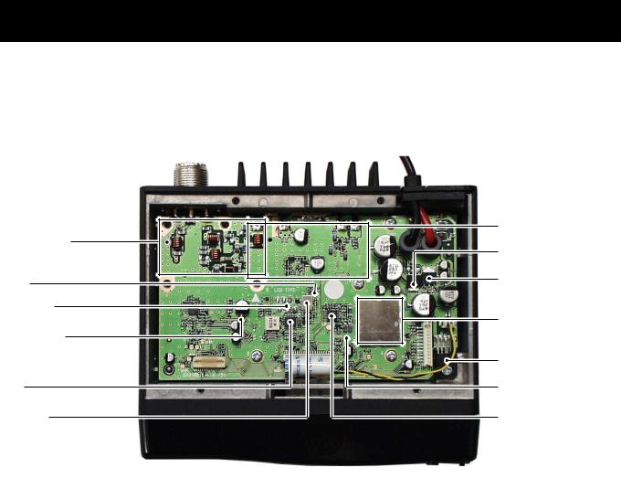
SECTION 2 |
INSIDE VIEW |
Antenna switch/
Low-pass filter circuit
Mixer*
(Q3: 3SK299) 2nd IF filter*
(FI2: ALFYM450F=K)
D/A converter*
(IC6: M62363FP-650C)
IF IC
(IC1: TA31136FN)
1st IF filter (FI1: FL-335)
* Located under side of the point.
Final FET module (IC3: S-AV33)
CPU 5V regurator* (IC10: AN78L05M)
8V regurator (IC9: TA7808F)
VCO circuit
AF amplifier (IC8: LA4425A)
Reference crystal oscillator* (X2: CR-740 15.3 MHz)
PLL IC
(IC4: MB15A02PFV-1)
2 - 1

SECTION 3 DISASSEMBLY INSTRUCTIONS
• Opening case
Unscrew 4 screws A, and remove the bottom cover.
Disconnect the flat cable B from J2.
Disconnect the cable C from J7.
Unscrew 2 screws D, and remove the front unit.
Lift up the front portion of the main unit and remove it.
 A
A
B
J2
J7 
C |
• Installation location
UT-105 SmarTrank 2 logic board UT-108 DTMF decoder unit
UT-109
Voice scrambler unit
UT-110
UT-111 Trunking unit
OPC-617 ACC cable (for external terminal connection)
D
Unscrew 8 screws E.
Remove the filter case F.
Unscrew the screw G.
Unsolder 3 points H from the antenna connector.
Unsolder 4 points I from IC3.
OPC-617 |
UT-105 |
UT-108 |
UT-109 |
UT-110 |
UT-111 |
J6 |
J1 |
E
F
H I
G
3 - 1

SECTION 4 CIRCUIT DESCRIPTION
4-1 RECEIVER CIRCUITS
4-1-1 ANTENNA SWITCHING CIRCUIT (MAIN UNIT)
The antenna switching circuit functions as a low-pass filter while receiving and as resonator circuit while transmitting. This circuit does not allow transmit signals to enter the receiver circuits.
Received signals enter the antenna connector and pass through the low-pass filters (L1–L3, C1, C2, C6–8). The filtered signals are then applied to the RF circuit passed through the λ⁄4 type antenna switching circuit (D5–D7, D48, L4, L6).
4-1-2 RF CIRCUIT (MAIN UNIT)
The RF circuit amplifies signals within the range of frequency coverage and filters out-of-band signals.
The signals from the antenna switching circuit pass through the two-stage tunable bandpass filters (D8, D4). The filtered signals are amplified at the RF amplifier (Q2) and then enter other two-stage bandpass filters (D9, D10) to suppress unwanted signals. The filtered signals are applied to the 1st mixer circuit (Q3).
The tunable bandpass filters (D4, D8–D10) employ varactor diodes to tune the center frequency of the RF passband for wide bandwidth receiving and good image response rejection. These diodes are controlled by the CPU (FRONT unit; IC1) via the D/A converter (IC6).
The gate control circuit reduces RF amplifier gain and attenuates RF signal to keep the audio output at a constant level.
The receiver gain is determined by the voltage on the “RSSI” line from the FM IF IC (IC1, pin 12). The gate control circuit (Q1) supplies control voltage to the RF amplifier (Q2) and sets the receiver gain.
4-1-3 1ST MIXER AND 1ST IF CIRCUITS (MAIN UNIT)
The 1st mixer circuit converts the received signals to a fixed frequency of the 1st IF signal with the PLL output frequency. By changing the PLL frequency, only the desired frequency will pass through a MCF (Monolithic Crystal Filter; FI1) at the next stage of the 1st mixer.
The RF signals from the bandpass filter are applied to the 1st mixer circuit (Q3). The applied signals are mixed with the 1st LO signal coming from the RX VCO circuit (Q14) to produce a 46.35 MHz 1st IF signal. The 1st IF signal passes through a MCF (Monolithic Crystal Filter; FI1) to suppress out-of-band signals. The filtered signal is amplified at the 1st IF amplifier (Q4) and applied to the 2nd IF circuit.
4-1-4 2ND IF AND DEMODULATOR CIRCUITS (MAIN UNIT)
The 2nd mixer circuit converts the 1st IF signal to a 2nd IF signal. A double-conversion superheterodyne system improves the image rejection ratio and obtains stable receiver gain.
The 1st IF signal from the 1st IF amplifier (Q4) is applied to the 2nd mixer section of the FM IF IC (IC1, pin 16) and is then mixed with the 2nd LO signal for conversion to a 450 kHz 2nd IF signal.
IC1 contains the 2nd mixer, limiter amplifier, quadrature detector, active filter and noise amplifier circuits, etc. A tripled frequency from the PLL reference oscillator is used for the 2nd LO signal (45.9 MHz).
The 2nd IF signal from the 2nd mixer (IC1, pin 3) passes through a ceramic filter (FI2) to remove unwanted heterodyned frequencies. It is then amplified at the limiter amplifier section (IC1, pin 5) and applied to the quadrature detector section (IC1, pins 10, 11 and X1) to demodulate the 2nd IF signal into AF signals.
When receiving strong signals, the “RSSI” voltage increases and the gate control voltage decreases. As the gate control voltage is used for the bias voltage of the RF amplifier (Q2), then the RF amplifier gain is decreased.
The AF signals are output from pin 9 (IC1) and are then applied to the AF amplifier circuit.
• 2ND IF AND DEMODULATOR CIRCUIT
|
|
|
2nd IF filter |
|
|
|
|
|
450 kHz |
45.9 MHz |
Q34 |
|
|
|
FI2 |
3 |
|
|
|
|
BPF |
||
8 |
7 |
5 |
3 |
2 |
X2 |
|
Active |
|
|
|
15.3 MHz |
|
filter |
Noise |
|
|
|
|
|
|
|
|
|
|
|
detector |
|
|
|
|
Limiter |
"SQLIN" signal |
amp. |
FM |
Mixer |
|
detector |
||
|
|
|
|
RSSI |
IC1 |
|
|
|
|
TA31136FN |
9 |
10 |
11 |
13 |
16 |
AF signals |
|
|
|
1st IF from the IF amplifier (Q4) |
|
|
|
|
|
|
|
5V |
|
"NOIS" signal to the CPU |
|
|
|
"RSSI" signal to the CPU |
|
|
X1 Discriminator |
|
||
4 - 1
4-1-5 AF AMPLIFIER CIRCUIT (MAIN UNIT)
The AF amplifier circuit amplifies the demodulated AF signals to drive a speaker.
The AF signals from the FM IF IC (IC1, pin 9) are applied to the active filter circuit (IC16). The active filter circuit (highpass filter) removes CTCSS or DTCS signals.
The filtered AF signals are output from pin 14 (IC16) and are applied to the de-emphasis circuit (R117, C378) with frequency characteristics of –6 dB/octave, and then passed through the analog switch (IC14, pins 1–3) and low-pass filter (IC5). The filtered signal is applied to the electronic volume controller (IC6, pin 9).
The output AF signals from the electronic volume controller (IC6, pin 10) are passed through the analog switch (IC14 pins 9–11) and are applied to the AF amplifier (IC15) and AF power amplifier (IC8) to drive the speaker.
4-1-6 RECEIVER MUTE CIRCUITS (MAIN AND FRONT UNITS)
• NOISE SQUELCH
The noise squelch circuit cuts out AF signals when no RF signals are received. By detecting noise components in the AF signals, the squelch circuit switches the AF mute switch.
Some noise components in the AF signals from the FM IF IC (IC1, pin 9) are passed through the level controller (IC6, pins 1, 2). The level controlled signals are applied to the active filter section in the FM IF IC (IC1, pin 8). Noise components about 10 kHz are amplified and output from pin 7.
The filtered signals are converted to the pulse-type signals at the noise detector section and output from pin 13 (NOIS).
The NOIS signal from the FM IF IC is applied to the CPU (FRONT unit; IC1, pin 53). The CPU then analyzes the noise condition and controls the AF mute signal via “AFON” line (D44, D45) to the AF mute circuit (Q35, Q36, D29, D30).
• CTCSS AND DTCS
The tone squelch circuit detects AF signals and opens the squelch only when receiving a signal containing a matching subaudible tone (CTCSS or DTCS). When tone squelch is in use, and a signal with a mismatched or no subaudible tone is received, the tone squelch circuit mutes the AF signals even when noise squelch is open.
A portion of the AF signals from the FM IF IC (IC1, pin 9) passes through the low-pass filter (IC16) to remove AF (voice) signals and is applied to the CTCSS or DTCS decoder inside the CPU (FRONT unit; IC1, pin 60) via the “CDEC” line to control the AF mute switch.
4-2 TRANSMITTER CIRCUITS
4-2-1 MICROPHONE AMPLIFIER CIRCUIT (MAIN AND FRONT UNITS)
The microphone amplifier circuit amplifies audio signals within +6 dB/octave pre-emphasis characteristics from the microphone to a level needed for the modulation circuit.
The AF signals (MIC) from the MIC jack (FRONT unit; J1) are amplified at the AF amplifier (FRONT unit; IC5) and applied to the MAIN unit via J2 (pin 28). The AF signal are applied to the limiter amplifier (IC5, pin 5).
The entered signals are pre-emphasized with +6dB/octave at a limiter amplifier, then passed through the analog switch (IC14, pins 2–4) and splatter filter (IC5, pins 2, 1). The output signals from the splatter filter are applied to the level controller (IC6, pin 9).
The deviation level controlled signals are then applied to the modulation circuit (D18) as the “MOD” signal after being passed through the analog switch (IC14, pins 9, 8).
4-2-2 MODULATION CIRCUIT (MAIN AND FRONT UNITS
The modulation circuit modulates the VCO oscillating signal (RF signal) using the microphone audio signals.
The AF signals from the analog switch (IC14, pin 8) change the reactance of varactor diode (D18) to modulate the oscillated signal at the TX VCO circuit (Q13, D16, D31). The modulated VCO signal is amplified at the buffer amplifiers (Q11, Q10) and is then applied to the drive amplifier circuit via the T/R switch (D14).
The CTCSS/DTCS signals from the CPU (FRONT unit; IC1, pins 22–24) are passed through the low-pass filter (FRONT unit; IC5), and mixer and splatter filter (IC5), and are then applied to the VCO circuit.
4-2-3 DRIVE AMPLIFIER CIRCUIT (MAIN UNIT)
The drive amplifier circuit amplifies the VCO oscillating signal to the level needed at the power amplifier.
The RF signal from the buffer amplifier (Q10) passes through the T/R switch (D14) and is amplified at the drive amplifier circuit (Q8). The amplified signal is applied to the power amplifier circuit.
4 - 2
4-2-4 POWER AMPLIFIER CIRCUIT (MAIN UNIT)
The power amplifier circuit amplifies the driver signal to an output power level.
The RF signal from the drive amplifier (Q8) is passed through the low-pass filter circuit (L18, L43, C89, C90, C92, C380, C381, C510) and applied to the power module (IC3) to obtain 25 W or 50 W of RF power.
The amplified signal is passed through the antenna switching circuit (D2), low-pass filter and APC detector, and is then applied to the antenna connector.
Control voltage for the power amplifier (IC3, pin 2) comes from the APC amplifier (IC2) to stabilize the output power. The transmit mute switch (D28) controls the APC amplifier when transmit mute is necessary.
4-2-5 APC CIRCUIT (MAIN UNIT)
The APC circuit protects the power amplifier from a mismatched output load and stabilizes the output power.
The APC detector circuit detects forward signals and reflection signals at D1 and D11 respectively. The combined voltage is at minimum level when the antenna impedance is matched at 50 Ω, and is increased when it is mismatched.
The detected voltage is applied to the APC amplifier (IC2, pin 3), and the power setting “T2” signal from the D/A converter (IC6, pin 22), controlled by the CPU (FRONT unit; IC1), is applied to the other input for reference. When antenna impedance is mismatched, the detected voltage exceeds the power setting voltage. Then the output voltage of the APC amplifier (IC2, pin 4) controls the input current of the drive amplifier (Q8) and power module (IC3) to reduce the output power.
• PLL CIRCUIT
4-3 PLL CIRCUITS
4-3-1 PLL CIRCUIT (MAIN UNIT)
A PLL circuit provides stable oscillation of the transmit frequency and receive 1st LO frequency. The PLL output compares the phase of the divided VCO frequency to the reference frequency. The PLL output frequency is controlled by the divided ratio (N-data) of a programable divider.
The PLL circuit contains the TX/RX VCO circuit (Q13, Q14). The oscillated signal is amplified at the buffer amplifiers (Q11, Q12) and then applied to the PLL IC (IC4, pin 8) via the low-pass filter (L32, C298–C300).
The PLL IC contains a prescaler, programable counter, programable divider and phase detector, etc. The entered signal is divided at the prescaler and programable counter section by the N-data ratio from the CPU. The reference signal is generated at the reference oscillator (X2) and is also applied to the PLL IC. The PLL IC detects the out-of-step phase using the reference frequency, and outputs it from pin 5. The output signal is passed through the loop filter (R97/C149, R96/C147), and is then applied to the VCO circuit as the lock voltage.
If the oscillated signal drifts, its phase changes from that of the reference frequency, causing a lock voltage change to compensate for the drift in the oscillated frequency.
4-3-2 VCO CIRCUIT (MAIN UNIT)
The VCO circuit contains a separate RX VCO (Q14, D33, D34) and TX VCO (Q13, D16, D18, D31). The oscillated signal is amplified at the buffer amplifiers (Q11, Q10) and is then applied to the T/R switch circuit (D14, D15). Then the receive 1st LO (Rx) signal is applied to the 1st mixer (Q3) and the transmit (Tx) signal to the drive amplifier circuit (Q8).
A portion of the signal from the buffer amplifier (Q11) is fed back to the PLL IC (IC4, pin 8) via the buffer amplifier (Q12) and low-pass filter (L32, C298–C300) as the comparison signal.
Loop
filter
2nd LO signal to the FM IF IC 45.9 MHz
X2
15.3 MHz
RX VCO |
|
|
|
|
|
D15 to 1st mixer circuit |
|
|
|
|
|
Buffer |
|
||
|
|
|
|
|
|
||
|
|
|
|
Q10 |
|
|
|
Q14, D33, D34 |
Buffer |
|
|
|
D14 to transmitter circuit |
||
|
|
|
|
|
|
||
TX VCO |
|
Q11 |
|
|
|
|
|
|
|
|
|
|
|
||
|
|
|
|
Buffer |
|
|
|
|
|
|
|
Q12 |
|
|
|
Q13, D18, D19, D31 |
|
|
|
|
|
||
|
|
|
IC4 MB15A02PFV1 |
|
|
||
5 |
Phase |
Programmable |
Prescaler |
8 |
|
||
|
detector |
counter |
|
|
|
||
|
|
|
|
|
|||
Tripler |
|
|
|
|
9 |
SCK |
|
Q34 |
Programmable |
|
|
||||
|
|
10 |
|
||||
×3 |
Shift register |
SO |
|||||
divider |
|
11 |
|||||
|
|
|
|
PLST |
|||
1 |
|
|
|
|
|
||
|
|
|
|
|
|
||
4 - 3
4-4 POWER SUPPLY CIRCUITS
4-4-1 VOLTAGE LINES (MAIN UNIT)
Line |
Description |
|
|
|
|
HV |
The voltage from a DC power supply. |
|
|
|
|
|
The same voltage as the HV line which is con- |
|
|
trolled by the power switching circuit (Q23, Q24). |
|
VCC |
When the [POWER] switch is pushed, the CPU |
|
|
outputs the “PWON” control signal to the power |
|
|
switching circuit to turn the circuit ON. |
|
|
|
|
|
Common 5 V for the CPU converted from the HV |
|
CPU5V |
line by the CPU5V regulator circuit (IC10). The |
|
circuit outputs the voltage regardless of the |
||
|
||
|
power ON/OFF condition. |
|
|
|
|
8V |
Common 8 V converted from the VCC line by the |
|
8V regulator circuit (IC9). |
||
|
||
|
|
|
5V |
Common 5 V converted from the 8 V and CPU5 |
|
lines by the 5V regulator circuit (Q27, Q28). |
||
|
||
|
|
|
|
Receive 8 V controlled by the R8 regulator circuit |
|
R8V |
(Q26, Q30) using the “RXC” signal from the |
|
|
expander IC (IC17, pin 4). |
|
|
|
|
|
Transmit 8 V controlled by the T8 regulator circuit |
|
T8V |
(Q25, Q29, D23) using the “TMUT” signal from |
|
|
the expander IC (IC17, pin 13). |
|
|
|
4-5 PORT ALLOCATIONS
4-5-1 CPU (FRONT UNIT; IC1)
Pin |
Port |
Description |
|
number |
name |
||
|
|||
|
|
|
|
1 |
TEMP |
Input port for the internal temperature. |
|
|
|
|
|
2 |
BATV |
Input port for the low voltage detection |
|
from the connected power supply. |
|||
|
|
||
|
|
|
|
7 |
RES |
Input port for reset signal. |
|
|
|
|
|
13–14 |
SENC0– |
Output ports for 5/2 tone and DTMF |
|
SENC1 |
signals. |
||
|
|||
|
|
|
|
15 |
CSFT |
Outputs the CPU clock shift signal. |
|
|
|
|
|
|
|
Outputs cut-off frequency control signal |
|
16 |
DUSE |
to the low-pass filter (MAIN unit; IC5) |
|
|
|
for CTCSS/DTCS switching. |
|
|
|
|
|
17, 18 |
KS0, KS1 |
Input port for the key matrix. |
|
|
|
|
|
19–20 |
SENC2– |
Output ports for 5/2 tone and DTMF |
|
SENC3 |
signals. |
||
|
|||
|
|
|
|
21 |
UNLK |
Input port for the PLL unlock signal |
|
from the PLL IC (MAIN unit; IC4). |
|||
|
|
||
|
|
|
|
22 |
KR0 |
Input port for the key matrix. |
|
|
|
|
|
23–25 |
CENO0– |
Output ports for CTCSS/DTCS signals. |
|
CENO2 |
|
||
|
|
||
|
|
|
|
26, 27 |
KR1, KR2 |
Input ports for the key matrix. |
|
|
|
|
|
|
|
Outputs the clock signal to the PLL IC |
|
28 |
SCK |
(MAIN unit; IC4), D/A converter (MAIN |
|
unit; IC6), LED driver (IC4) and option- |
|||
|
|
||
|
|
al board (connect to MAIN unit; J1). |
|
|
|
|
|
|
|
Outputs the data signal to the PLL IC |
|
29 |
SO |
(MAIN unit; IC4), D/A converter (MAIN |
|
unit; IC6) and optional board (connect |
|||
|
|
||
|
|
to MAIN unit; J1). |
|
|
|
|
|
30 |
BEEP |
Output port for beep sound signal. |
|
|
|
|
|
31 |
ESDA |
I/O port for the data signal for the EEP- |
|
ROM (IC3) |
|||
|
|
||
|
|
|
|
32 |
ESCL |
Outputs the clock signal for the EEP- |
|
ROM (IC3). |
|||
|
|
||
|
|
|
|
33 |
LSCK |
Outputs the clock signal for the LCD |
|
driver (IC6, pin 17). |
|||
|
|
||
|
|
|
|
34 |
LSO |
Outputs the data signal for the LCD dri- |
|
ver (IC6, pin 48). |
|||
|
|
||
|
|
|
|
36 |
PLST |
Outputs the strobe signal for the PLL |
|
IC (MAIN unit; IC4). |
|||
|
|
||
|
|
|
|
37 |
DAST |
Outputs the strobe signal for the D/A |
|
converter IC (MAIN unit; IC6). |
|||
|
|
||
|
|
|
|
38 |
EXST |
Outputs the strobe signal for the |
|
expander IC (IC17). |
|||
|
|
||
|
|
|
|
39 |
EXOE |
Outputs the control signal for the LCD |
|
driver IC (IC6). |
|||
|
|
||
|
|
|
|
|
|
Outputs the control signal for the power |
|
41 |
PWON |
switching circuit (MAIN unit; Q24, |
|
|
|
Q23). |
|
|
|
|
4 - 4
CPU-Continued
Pin |
Port |
Description |
|
number |
name |
|
|
|
|
||
|
|
|
|
44–46 |
OPT3– |
I/O ports for the optional board control |
|
OPT1 |
signals. |
|
|
|
|
||
|
|
|
|
48 |
SI |
Input port for the clock sigal from the |
|
optional board via J1. |
|
||
|
|
|
|
|
|
|
|
49 |
CLI |
Input port for the cloning signal. |
|
|
|
|
|
50 |
CLO |
Output port for the cloning signal. |
|
|
|
|
|
51 |
POSW |
Input port for the POWER switch. |
|
|
|
|
|
|
|
• Input port for the remote power con- |
|
52 |
IGSW |
trol signal from the external connec- |
|
tor.(J6) |
|
||
|
|
|
|
|
|
• Input port for the dimmer control. |
|
|
|
|
|
|
|
Input port for the “NOIS” signal from |
|
83 |
NOIS |
the FM IF IC (MAIN unit; IC1) for noise |
|
|
|
squelch operation. |
|
|
|
|
|
54 |
CIRQ |
Input port for interruption signal |
from |
the optional board via J1. |
|
||
|
|
|
|
|
|
|
|
55 |
CCS |
Outputs chip select signal for |
the |
optional board via J1. |
|
||
|
|
|
|
|
|
|
|
56 |
PTT |
Input port for the PTT switch |
from |
microphone. |
|
||
|
|
|
|
|
|
|
|
|
|
Input port for the PTT switch from the |
|
57 |
EPTT |
external connector (J6). |
|
|
|
Low : External PTT switch is ON. |
|
|
|
|
|
|
|
Input port for the microphone hanger |
|
58 |
HANG |
detection signal. |
|
|
|
Low : Microphone on hook. |
|
|
|
|
|
|
|
Input port for the AF volume control |
|
59 |
AFVI |
signal (R14). |
|
|
|
High : [VOL] is maximum clockwise. |
|
|
|
|
|
60 |
CDEC |
Input port for the CTCSS/DTCS decod- |
|
ing signals. |
|
||
|
|
|
|
|
|
|
|
61 |
SDEC |
Input port for the single tone decoding |
|
signal. |
|
||
|
|
|
|
|
|
|
|
62 |
OPV1V2 |
Input port for the optional board detec- |
|
tion signal. |
|
||
|
|
|
|
63 |
RSSI |
Input port for receiving signal strength |
|
level detection. |
|
||
|
|
|
|
|
|
|
|
64 |
LVIN |
Input port for the PLL lock voltage. |
|
|
|
|
|
4-5-2 OUTPUT EXPANDER (MAIN UNIT; IC17)
Pin |
Port |
Description |
|
number |
name |
||
|
|||
|
|
|
|
4 |
RXC |
Outputs transmit/receive control signal. |
|
|
|
High: While receiving. |
|
|
|
|
|
5 |
AFON |
Outputs audio output control signal. |
|
|
|
High: While receiving. |
|
|
|
|
|
6 |
NWC |
Outputs wide/narrow control signal. |
|
|
|
High: Wide is selected. |
|
|
|
|
|
7 |
RMUT |
Outputs receiving mute control signal. |
|
|
|
Low: While receiving is muting. |
|
|
|
|
|
|
|
Outputs transmitting mute control sig- |
|
13 |
TMUT |
nal. |
|
|
|
Low: While transmitting is muting. |
|
|
|
|
|
|
|
Outputs the microphone mute control |
|
14 |
MMUT |
signal. |
|
|
|
Low: While the microphone is muting. |
|
|
|
|
4-5-3 LCD DRIVER (FRONT UNIT; IC6)
Pin |
Port |
Description |
|
number |
name |
||
|
|||
|
|
|
|
1 |
LIGT1 |
Outputs dimmer control signal. |
|
|
High: Dimmter is ON. |
||
|
|
||
|
|
|
|
2 |
LIGT2 |
Outputs backlight control signal. |
|
|
High: Backlight is ON. |
||
|
|
||
|
|
|
|
3–34 |
SEG32– |
Output LCD segment signals. |
|
|
SEG1 |
|
|
35–38 |
COM4– |
Output LCD common signals. |
|
COM1 |
|||
|
|
||
|
|
|
4 - 5
Loading...