


Hitachi HDP725016GLAT80, CINEMASTAR P7K500, HDP725016GLA380, HDP725025GLAT80, HDP725025GLA380/1 Specification
...Hitachi Global Storage Technologies
Hard Disk Drive Specification
Hitachi Deskstar P7K500 Hitachi CinemaStar P7K500
3.5 inch hard disk drive
Models: HDP725016GLAT80 |
HCP725016GLAT80 |
HDP725016GLA380 |
HCP725016GLA380 |
HDP725025GLAT80 |
HCP725025GLAT80 |
HDP725025GLA380/1 |
HCP725025GLA380 |
HDP725032GLAT80 |
HCP725032GLAT80 |
HDP725032GLA380 |
HCP725032GLA380 |
HDP725032GLA360/1 |
HCP725050GLAT80 |
HDP725040GLAT80 |
HCP725050GLA380 |
HDP725040GLA380 |
|
HDP725040GLA360/1 |
|
HDP725050GLAT80 |
|
HDP725050GLA380 |
|
HDP725050GLA360/1 |
|
Revision 1.0 (November 14, 2007)
The following paragraph does not apply to the United Kingdom or any country where such provisions are inconsistent with local law: HITACHI GLOBAL STORAGE TECHNOLOGIES Inc. PROVIDES THIS PUBLICATION “AS IS” WITHOUT WARRANTY OF ANY KIND, EITHER EXPRESS OR IMPLIED, INCLUDING, BUT NOT LIMITED TO, THE IMPLIED WARRANTIES OF MERCHANTABILITY OR FITNESS FOR A PARTICULAR PURPOSE. Some states do not allow disclaimer or express or implied warranties in certain transactions, therefore, this statement may not apply to you.
This publication could include technical inaccuracies or typographical errors. Changes are periodically made to the information herein; these changes will be incorporated in new editions of the publication. Hitachi Global Storage Technologies may make improvements or changes in any products or programs described in this publication at any time.
It is possible that this publication may contain reference to, or information about, Hitachi Global Storage Technologies products (machines and programs), programming, or services that are not announced in your country. Such references or information must not be construed to mean that Hitachi Global Storage Technologies intends to announce such Hitachi Global Storage Technologies products, programming, or services in your country.
Technical information about this product is available by contacting your local Hitachi Global Storage Technologies representative or on the
|Internet at
http://www.HitachiGST.com/
Hitachi Global Storage Technologies may have patents or pending patent applications covering subject matter in this document. The furnishing of this document does not give you any license to these patents. You can send license inquiries in writing to the Hitachi Global Storage Technologies Director of Commercial Relations, Hitachi Global Storage Technologies Inc. , San Jose, CA .
©Copyright Hitachi Global Storage Technologies 2004. All rights reserved.
Note to U.S. Government Users —Documentation related to restricted rights —Use, duplication or disclosure is subject to restrictions set forth in GSA ADP Schedule Contract with Hitachi Global Storage Technologies Inc.
HITACHI Deskstar & CinemaStar P7K500 Hard Disk Drive specification (Rev 1.1) i

Table of contents
1.0 |
General.................................................................................................................................................... |
2 |
|
|
1.1 |
Introduction.............................................................................................................................. |
2 |
|
1.2 |
Glossary.................................................................................................................................... |
2 |
|
1.3 |
Caution ..................................................................................................................................... |
2 |
|
1.4 |
References ................................................................................................................................ |
2 |
2.0 |
General features...................................................................................................................................... |
3 |
|
Part 1. Functional specification ................................................................................................................ |
5 |
||
3.0 Fixed disk subsystem description ............................................................................................................ |
7 |
||
|
3.1 |
Control Electronics .................................................................................................................. |
7 |
|
3.2 |
Head disk assembly ................................................................................................................. |
7 |
|
3.3 |
Actuator.................................................................................................................................... |
7 |
4.0 |
Drive characteristics ................................................................................................................................ |
8 |
|
|
4.1 |
Default logical drive parameters............................................................................................. |
8 |
|
4.2 |
Data sheet ................................................................................................................................ |
9 |
|
|
P |
|
|
4.3 |
World Wide Name Assignment................................................................................................ |
9 |
|
4.4 |
Drive organization ................................................................................................................... |
9 |
|
4.5 |
Performance characteristics .................................................................................................. |
10 |
5.0 |
Defect flagging strategy ......................................................................................................................... |
14 |
|
|
5.1 |
Electrical interface................................................................................................................. |
15 |
|
5.2 |
Signal timings ........................................................................................................................ |
22 |
|
5.3 |
Jumper settings(PATA model) ............................................................................................... |
35 |
|
5.4 |
Environment .......................................................................................................................... |
41 |
|
5.5 |
DC power requirements......................................................................................................... |
43 |
|
5.6 |
Reliability ............................................................................................................................... |
46 |
|
5.7 |
Mechanical specifications ...................................................................................................... |
47 |
|
5.8 |
Vibration and shock ............................................................................................................... |
52 |
|
5.9 |
Acoustics................................................................................................................................. |
54 |
|
5.10 |
Identification labels ............................................................................................................... |
54 |
|
5.11 |
Safety...................................................................................................................................... |
55 |
|
5.12 |
Electromagnetic compatibility............................................................................................... |
56 |
Part 2. Interface Specification................................................................................................................. |
57 |
||
6.0 |
General.................................................................................................................................................. |
58 |
|
|
6.1 |
Introduction............................................................................................................................ |
58 |
|
6.2 |
Terminology............................................................................................................................ |
58 |
|
6.3 |
Deviations From Standard .................................................................................................... |
58 |
7.0 |
Registers ............................................................................................................................................... |
59 |
|
|
7.1 |
Alternate Status Register...................................................................................................... |
59 |
|
7.2 |
Command register.................................................................................................................. |
59 |
|
7.3 |
Cylinder High Register.......................................................................................................... |
59 |
|
7.4 |
Cylinder Low Register ........................................................................................................... |
59 |
|
7.5 |
Data Register ......................................................................................................................... |
60 |
|
7.6 |
Device Control Register ......................................................................................................... |
60 |
|
7.7 |
Drive Address Register .......................................................................................................... |
60 |
|
7.8 |
Device/Head Register............................................................................................................. |
61 |
|
7.9 |
Error Register ........................................................................................................................ |
62 |
|
7.10 |
Features Register................................................................................................................... |
62 |
|
7.11 |
Sector Count Register............................................................................................................ |
62 |
|
7.12 |
Sector Number Register ........................................................................................................ |
62 |
|
7.13 |
Status Register....................................................................................................................... |
62 |
8.0 |
General Operation Descriptions............................................................................................................. |
64 |
|
|
8.1 |
Reset Response....................................................................................................................... |
64 |
|
8.2 |
Diagnostic and Reset considerations .................................................................................... |
65 |
|
8.3 |
Sector Addressing Mode......................................................................................................... |
66 |
|
8.4 |
Power Management Feature ................................................................................................. |
67 |
|
8.5 |
SMART Function ................................................................................................................... |
68 |
|
8.6 |
Security Mode Feature Set.................................................................................................... |
70 |
HITACHI Deskstar & CinemaStar P7K500 Hard Disk Drive specification (Rev 1.1) ii
|
8.7 |
Host Protected Area Feature................................................................................................. |
76 |
|
8.8 |
Seek Overlap .......................................................................................................................... |
78 |
|
8.9 |
Write Cache Function ............................................................................................................ |
78 |
|
8.10 |
Reassign Function.................................................................................................................. |
79 |
|
8.11 |
Power-up in Standby feature set........................................................................................... |
80 |
|
8.12 |
Advanced Power Management feature set (APM)................................................................ |
80 |
|
8.13 |
Automatic Acoustic Management feature set (AAM) ........................................................... |
81 |
|
8.14 |
Address Offset Feature.......................................................................................................... |
81 |
|
8.15 |
48-bit Address Feature Set.................................................................................................... |
83 |
|
8.16 |
Streaming feature Set............................................................................................................ |
84 |
|
8.17 |
SATA BIST (Built-in Self Test).............................................................................................. |
86 |
|
8.18 |
SATA Interface Power Management ..................................................................................... |
86 |
|
8.19 |
Software Setting Preservation .............................................................................................. |
87 |
|
8.20 |
SATA II Optional Features .................................................................................................... |
88 |
|
8.21 |
SCT Command Transport feature Set .................................................................................. |
92 |
9.0 |
Command Protocol............................................................................................................................... |
111 |
|
|
9.1 PIO Data In commands ........................................................................................................ |
111 |
|
|
9.2 PIO Data Out commands...................................................................................................... |
111 |
|
|
9.3 |
Non-Data commands ............................................................................................................ |
112 |
|
9.4 DMA Data In commands and DMA Data Out commands................................................... |
112 |
|
|
9.5 |
First-party DMA commands................................................................................................. |
113 |
10.0 |
Command Descriptions ........................................................................................................................ |
115 |
|
|
10.1 |
Check Power Mode (E5h/98h) .............................................................................................. |
119 |
|
10.2 ................................................................................................................................................... |
Configure Stream (51h) |
119 |
|
10.3 |
120 |
|
|
10.4 |
Device Configuration Overlay (B1h) .................................................................................... |
122 |
|
10.5 |
Download Microcode (92h).................................................................................................... |
126 |
|
10.6 |
Execute Device Diagnostic (90h) .......................................................................................... |
128 |
|
10.7 |
Flush Cache (E7h)................................................................................................................. |
129 |
|
10.8 |
Flush Cache Ext (EAh) ......................................................................................................... |
130 |
|
10.9 |
Format Track (50h) ............................................................................................................... |
131 |
|
10.10 |
Format Unit (F7h)............................................................................................................. |
133 |
|
10.11 |
Identify Device (ECh)........................................................................................................ |
134 |
|
10.12 |
Idle (E3h/97h) .................................................................................................................... |
145 |
|
10.13 |
Idle Immediate (E1h/95h) ................................................................................................. |
147 |
|
10.14 |
Initialize Device Parameters (91h)................................................................................... |
148 |
|
10.15 |
Read Buffer (E4h).............................................................................................................. |
149 |
|
10.16 |
Read DMA(C8h/C9h)......................................................................................................... |
150 |
|
10.17 |
Read DMA Ext (25h) ......................................................................................................... |
152 |
|
10.18 |
Read FPDMA Queued (60h).............................................................................................. |
154 |
|
10.19 |
Read Log Ext (2Fh) ........................................................................................................... |
156 |
|
10.20 |
Read Multiple (C4h) .......................................................................................................... |
169 |
|
10.21 |
Read Multiple Ext (29h).................................................................................................... |
170 |
|
10.22 |
Read Native Max Address (F8h)....................................................................................... |
172 |
|
10.23 |
Read Native Max Address Ext (27h) ................................................................................ |
173 |
|
10.24 |
Read Sector(s) (20h/21h) ................................................................................................... |
175 |
|
10.25 |
Read Sector(s) Ext (24h).................................................................................................... |
177 |
|
10.26 |
Read Stream DMA (2Ah)................................................................................................... |
179 |
|
10.27 |
Read Stream PIO (2Bh) .................................................................................................... |
182 |
|
10.28 |
Read Verify Sector(s) (40h/41h) ........................................................................................ |
184 |
|
10.29 |
Read Verify Sector(s) Ext (42h)......................................................................................... |
186 |
|
10.30 |
Recalibrate (1xh) ............................................................................................................... |
188 |
|
10.31 |
Security Disable Password (F6h)...................................................................................... |
189 |
|
10.32 |
Security Erase Prepare (F3h) ........................................................................................... |
191 |
|
10.33 |
Security Erase Unit (F4h)................................................................................................. |
192 |
|
10.34 |
Security Freeze Lock (F5h) ............................................................................................... |
194 |
|
10.35 |
Security Set Password (F1h)............................................................................................. |
195 |
|
10.36 |
Security Unlock (F2h) ....................................................................................................... |
197 |
HITACHI Deskstar & CinemaStar P7K500 Hard Disk Drive specification (Rev 1.1) iii
10.37 |
Seek (7xh) .......................................................................................................................... |
199 |
10.38 |
Set Features (EFh) ............................................................................................................ |
200 |
10.39 |
Set Max Address (F9h)...................................................................................................... |
205 |
10.40 |
Set Max Address Ext (37h) ............................................................................................... |
211 |
10.41 |
Set Multiple (C6h) ............................................................................................................. |
213 |
10.42 |
Sleep (E6h/99h) ................................................................................................................. |
214 |
10.43 |
SMART Function Set (B0h) .............................................................................................. |
215 |
10.44 |
Standby (E2h/96h)............................................................................................................. |
233 |
10.45 |
Standby Immediate (E0h/94h).......................................................................................... |
235 |
10.46 |
Write Buffer (E8h)............................................................................................................. |
236 |
10.47 |
Write DMA (Cah/CBh)....................................................................................................... |
237 |
10.48 |
Write DMA FUA Ext (3Dh) ............................................................................................... |
239 |
10.49 |
Write DMA Ext (35h)......................................................................................................... |
241 |
10.50 |
Write FPDMA Queued (61h)............................................................................................. |
243 |
10.51 |
Write Log Ext (3Fh)........................................................................................................... |
245 |
10.52 |
Write Multiple (C5h) ......................................................................................................... |
247 |
10.53 |
Write Multiple Ext (39h)................................................................................................... |
249 |
10.54 |
Write Multiple FUA Ext (CEh) ......................................................................................... |
251 |
10.55 |
Write Sector(s) (30h/31h) .................................................................................................. |
253 |
10.56 |
Write Sector(s) Ext (34h)................................................................................................... |
255 |
10.57 |
Write Stream DMA (3Ah).................................................................................................. |
257 |
10.58 |
Write Stream PIO (3Bh).................................................................................................... |
260 |
10.59 |
Write Uncorrectable Ext (45h).......................................................................................... |
263 |
11.0 Timings ................................................................................................................................................ |
266 |
|
HITACHI Deskstar & CinemaStar P7K500 Hard Disk Drive specification (Rev 1.1) iv

List of tables |
|
|
Table 1 Formatted capacity................................................................................................................ |
8 |
|
Table 2 Mechanical positioning performance ................................................................................. |
9 |
|
Table 3 World Wide Name Assignment........................................................................................... |
9 |
|
Table 4 |
Command overhead .......................................................................................................... |
10 |
Table 5 Mechanical positioning performance ................................................................................ |
11 |
|
Table 6 Full stroke seek time ......................................................................................................... |
11 |
|
Table 7 Single Track Seek Time ..................................................................................................... |
11 |
|
Table 8 |
Latency Time..................................................................................................................... |
12 |
Table 9 Drive ready time ............................................................................................................... |
12 |
|
Table 10 Mode transition times..................................................................................................... |
13 |
|
Table 11 Table of signals................................................................................................................ |
17 |
|
Table 12 Signal special definitions for Ultra DMA....................................................................... |
17 |
|
Table 13 Interface connector pins and I/O signals........................................................................ |
20 |
|
Table 14 |
Parameter descriptions................................................................................................... |
21 |
Table 15 System reset timing ........................................................................................................ |
22 |
|
Table 16 PIO cycle timings ............................................................................................................ |
23 |
|
Table 17 Multiword DMA cycle timings........................................................................................ |
25 |
|
Table 18 Ultra DMA cycle timings (Initiating Read) ................................................................... |
26 |
|
Table 19 Ultra DMA cycle timings (Host pausing Read) ............................................................. |
27 |
|
Table 20 Ultra DMA cycle timings (Host terminating Read)....................................................... |
28 |
|
Table 21 Ultra DMA cycle timings (Device Terminating Read)................................................... |
29 |
|
Table 22 Ultra DMA cycle timings (Initiating Write)................................................................... |
30 |
|
Table 23 Ultra DMA cycle timings (Device Pausing Write)......................................................... |
31 |
|
Table 24 Ultra DMA cycle timings (Device terminating Write)................................................... |
32 |
|
Table 25 Ultra DMA cycle timings (Host Terminating Write)..................................................... |
33 |
|
Table 26 I/O address map .............................................................................................................. |
34 |
|
Table 27 Temperature and humidity ............................................................................................ |
41 |
|
Table 28 |
Input voltage ................................................................................................................... |
43 |
Table 29 Power supply current of 2 Disk PATA models............................................................... |
43 |
|
Table 30 Power supply current of 1 Disk PATA models............................................................... |
44 |
|
Table 31 Power supply current of 2 Disk SATA models............................................................... |
44 |
|
Table 32 Power supply current of 1 Disk SATA models............................................................... |
45 |
|
Table 33 Power supply generated ripple at drive power connector ............................................. |
45 |
|
Table 34 |
Physical Dimensions ....................................................................................................... |
48 |
Table 35 Random vibration PSD profile break points (operating)............................................... |
52 |
|
Table 36 Random vibration PSD profile break points (nonoperating)......................................... |
52 |
|
Table 37 Sinusoidal shock wave .................................................................................................... |
53 |
|
Table 38 |
Rotational Shock ............................................................................................................. |
53 |
Table 39 Sound power levels.......................................................................................................... |
54 |
|
Table 40 Alternate Status Register............................................................................................... |
59 |
|
Table 41 Device Control Register .................................................................................................. |
60 |
|
Table 42 Drive Address Register ................................................................................................... |
60 |
|
Table 43 |
Device/Head Register...................................................................................................... |
61 |
Table 44 |
Error Register ................................................................................................................. |
62 |
Table 45 |
Status Register................................................................................................................ |
63 |
Table 46 |
Reset Response................................................................................................................ |
64 |
Table 47 Default Register Values.................................................................................................... |
65 |
|
Table 48 |
Diagnostic Codes ............................................................................................................. |
65 |
Table 49 |
Power conditions .............................................................................................................. |
68 |
Table 50 Command table for device lock operation - 1 ................................................................. |
74 |
|
Table 51 Command table for device lock operation - 2 ................................................................. |
75 |
|
Table 52 Phy Event Counter Identifiers ........................................................................................... |
89 |
|
Table 53 READ LOG EXT Log Page 11h data structure definition............................................. |
90 |
|
Table 54 SCT Log Page and direction............................................................................................. |
92 |
|
|
HITACHI Deskstar & CinemaStar P7K500 Hard Disk Drive specification (Rev 1.1) |
|
|
v |
|
Table 55 Identify Device Information Word 206........................................................................... |
92 |
|
Table 56 Output Registers of SCT Command Using SMART...................................................... |
93 |
|
Table 57 Input Registers of SCT Command Using SMART......................................................... |
93 |
|
Table 58 Input Registers of SCT Command Using Write Log Ext............................................... |
94 |
|
Table 59 Output Registers of SCT Command Using Write Log Ext............................................ |
94 |
|
Table 60 Key Sector Format............................................................................................................ |
95 |
|
Table 61 |
SCT Action Code List........................................................................................................ |
95 |
Table 62 Extended Status Code...................................................................................................... |
96 |
|
Table 63 Input Registers of SCT Data Transfer Using SMART .................................................. |
97 |
|
Table 64 Input Registers of SCT Data Transfer using Read/Write Log Ext................................ |
97 |
|
Table 65 Intput Registers of SCT Status Request Using SMART ............................................... |
98 |
|
Table 66 Input Registers of SCT Status Request Using Read Log Ext ....................................... |
98 |
|
Table 67 Data Format of SCT Status Response........................................................................... |
100 |
|
Table 68 |
LBA Segment Access (Inputs)........................................................................................ |
101 |
Table 69 |
LBA Segment Access (Outputs)..................................................................................... |
101 |
Table 70 Error Recovery Control command (Inputs)................................................................... |
104 |
|
Table 71 Error Recovery Control command (Onputs) ................................................................. |
104 |
|
Table 72 Feature Control command (Inputs)............................................................................... |
105 |
|
Table 73 Feature Control command (Outputs)............................................................................ |
105 |
|
Table 74 Feature Code List ............................................................................................................ |
106 |
|
Table 75 SCT Data Table command (Inputs)............................................................................... |
107 |
|
Table 76 SCT Data Table command (Outputs) ............................................................................ |
107 |
|
Table 77 |
Table ID ........................................................................................................................... |
107 |
Table 78 Data Format of HDA Absolute Temperature History Table......................................... |
109 |
|
Table 79 |
Command Set.................................................................................................................. |
115 |
Table 80 |
Command Set --Continued--............................................................................................ |
116 |
Table 81 Command Set (Subcommand) ........................................................................................ |
117 |
|
Table 82 Check Power Mode Command (E5h/98h)...................................................................... |
119 |
|
Table 83 Configure Stream Command (51h).................................................................................. |
120 |
|
Table 84 Device Configuration Overlay Command (B1h) ........................................................... |
122 |
|
Table 85 Device Configuration Overlay Features register values .............................................. |
122 |
|
Table 86 Device Configuration Overlay Data structure.............................................................. |
124 |
|
Table 87 DCO error information definition ...................................................................................... |
125 |
|
Table 88 Download Microcode Command (92h)S........................................................................... |
126 |
|
Table 89 Execute Device Diagnostic Command (90h) ................................................................. |
128 |
|
Table 90 Flush Cache Command (E7h) ......................................................................................... |
129 |
|
Table 91 Flush Cache Ext Command (EAh)................................................................................... |
130 |
|
Table 92 Format Track Command(50h)....................................................................................... |
131 |
|
Table 93 Format Unit Command (F7h)........................................................................................... |
133 |
|
Table 94 Identify Device Command (ECh) ..................................................................................... |
134 |
|
Table 95 Identify device information............................................................................................ |
135 |
|
Table 96 Identify device information --Continued--..................................................................... |
136 |
|
Table 97 Identify device information --Continued— ................................................................... |
137 |
|
Table 98 Identify device information --Continued--..................................................................... |
138 |
|
Table 99 Identify device information --Continued--..................................................................... |
139 |
|
Table 100 Identify device information --Continued--................................................................... |
140 |
|
Table 101 Identify device information --Continued--................................................................... |
141 |
|
Table 102 Identify device information --Continued--................................................................... |
142 |
|
Table 103 Identify device information --Continued--................................................................... |
143 |
|
Table 104 Identify device information --Continued--................................................................... |
144 |
|
Table 105 Idle Command (E3h/97h)............................................................................................... |
145 |
|
Table 106 Idle Immediate Command (E1h/95h)............................................................................. |
147 |
|
Table 107 Initialize Device Parameters Command (91h)............................................................ |
148 |
|
Table 108 Read Buffer Command (E4h) ........................................................................................ |
149 |
|
Table 109 Read DMA Command (C8h/C9h) .................................................................................. |
150 |
|
Table 110 Read DMA Ext Command (25h) .................................................................................... |
152 |
|
Table 111 Read FPDMA Queued Command (60h) ........................................................................ |
154 |
|
Table 112 Read Log Ext Command (2Fh) ...................................................................................... |
156 |
|
|
HITACHI Deskstar & CinemaStar P7K500 Hard Disk Drive specification (Rev 1.1) |
|
|
vi |
|
Table 113 Log Address Definition................................................................................................... |
157 |
Table 114 General Purpose Log Directory ..................................................................................... |
158 |
Table 115 Extended Comprehensive SMART Error Log............................................................. |
159 |
Table 116 Extended Error log data structure .................................................................................. |
160 |
Table 117 Command data structure ............................................................................................... |
160 |
Table 118 Error data structure........................................................................................................ |
161 |
Table 119 Extended Self-test log data structure.......................................................................... |
162 |
Table 120 Extended Self-test log descriptor entry....................................................................... |
163 |
Table 121 Command Error information .......................................................................................... |
164 |
Table 122 Read Stream Error Log................................................................................................ |
165 |
Table 123 Stream Error Log entry ............................................................................................... |
166 |
Table 124 Write Stream Error Log............................................................................................... |
167 |
Table 125 Streaming Performance Parameters log..................................................................... |
168 |
Table 126 Sector Time Array Entry (Linearly Interpolated)....................................................... |
168 |
Table 127 Position Array Entry (Linearly Interpolated)............................................................. |
168 |
Table 128 Access Time Array Entry (Linearly Interpolated) ...................................................... |
168 |
Table 129 Read Multiple Command (C4h) ..................................................................................... |
169 |
Table 130 Read Multiple Ext Command (29h)................................................................................ |
170 |
Table 131 Read Native Max ADDRESS (F8h) ............................................................................... |
172 |
Table 132 Read Native Max Address Ext (27h) ............................................................................. |
173 |
Table 133 Read Sector(s) Command (20h/21h)............................................................................. |
175 |
Table 134 Read Sector(s) Ext Command (24h) ............................................................................. |
177 |
Table 135 Read Stream DMA Command (2Ah) ........................................................................... |
179 |
Table 136 Read Stream PIO Command (2Bh) ............................................................................. |
182 |
Table 137 Read Verify Sector(s) Command (40h/41h)................................................................. |
184 |
Table 138 Read Verify Sector(s) Ext Command (42h) ................................................................. |
186 |
Table 139 Recalibrate Command (1xh).......................................................................................... |
188 |
Table 140 Security Disable Password Command (F6h) .............................................................. |
189 |
Table 141 Password Information for Security Disable Password command .............................. |
190 |
Table 142 Security Erase Prepare Command (F3h) .................................................................... |
191 |
Table 143 Security Erase Unit Command (F4h)............................................................................. |
192 |
Table 144 Erase Unit Information................................................................................................... |
193 |
Table 145 Security Freeze Lock Command (F5h).......................................................................... |
194 |
Table 146 Security Set Password Command (F1h) ..................................................................... |
195 |
Table 147 Security Set Password Information................................................................................ |
196 |
Table 148 Security Unlock Command (F2h)................................................................................... |
197 |
Table 149 Security Unlock Information........................................................................................... |
198 |
Table 150 Seek Command (7xh).................................................................................................... |
199 |
Table 151 Set Features Command (EFh)....................................................................................... |
200 |
Table 152 Set Max ADDRESS (F9h).............................................................................................. |
205 |
Table 153 Set Max set Password................................................................................................... |
207 |
Table 154 Set Max Set Password data contents............................................................................ |
207 |
Table 155 Set Max Lock................................................................................................................. |
208 |
Table 156 Set Max Unlock (F9h).................................................................................................... |
209 |
Table 157 Set Max Freeze Lock (F9h) ........................................................................................... |
210 |
Table 158 Set Max Address Ext Command (37h) .......................................................................... |
211 |
Table 159 Set Multiple Command (C6h) ........................................................................................ |
213 |
Table 160 Sleep Command (E6h/99h) ........................................................................................... |
214 |
Table 161 SMART Function Set Command (B0h).......................................................................... |
215 |
Table 162 Log sector addresses .................................................................................................... |
218 |
Table 163 Device Attribute Data Structure ..................................................................................... |
220 |
Table 164 Individual Attribute Data Structure........................................................................... |
221 |
Table 165 Device Attribute Thresholds Data Structure.............................................................. |
225 |
Table 166 Individual Threshold Data Structure ......................................................................... |
225 |
Table 167 SMART Log Directory.................................................................................................... |
226 |
Table 168 SMART summary error log sector ................................................................................. |
227 |
Table 169 Error log data structure.................................................................................................. |
228 |
Table 170 Command data structure ............................................................................................... |
228 |
HITACHI Deskstar & CinemaStar P7K500 Hard Disk Drive specification (Rev 1.1) |
|
vii |
|
Table 171 Error data structure........................................................................................................ |
229 |
Table 172 Self-test log data structure............................................................................................. |
230 |
Table 173 Selective self-test log data structure ........................................................................... |
231 |
Table 174 Selective self-test feature flags.................................................................................... |
231 |
Table 175 SMART Error Codes...................................................................................................... |
232 |
Table 176 Standby Command (E2h/96h) ....................................................................................... |
233 |
Table 177 Standby Immediate Command (E0h/94h)................................................................... |
235 |
Table 178 Write Buffer Command (E8h) ........................................................................................ |
236 |
Table 179 Write DMA Command (Cah/CBh).................................................................................. |
237 |
Table 180 Write DMA FUA Ext Command (3Dh) ........................................................................... |
239 |
Table 181 Write DMA Ext Command (35h) .................................................................................... |
241 |
Table 182 Write FPDMA Queued Command (61h) ........................................................................ |
243 |
Table 183 Write Log Ext Command (3Fh) ...................................................................................... |
245 |
Table 184 Write Multiple Command (C5h) ..................................................................................... |
247 |
Table 185 Write Multiple Ext Command (39h)................................................................................ |
249 |
Table 186 Write Multiple FUA Ext Command (CEh).................................................................. |
251 |
Table 187 Write Sector(s) Command (30h/31h)............................................................................. |
253 |
Table 188 Write Sector(s) Ext Command (34h).............................................................................. |
255 |
Table 189 Write Stream DMA Command (3Ah)........................................................................... |
257 |
Table 190 Write Stream PIO Command (3Bh) ............................................................................ |
260 |
Table 191 Write Uncorrectable Ext Command (45h)................................................................... |
263 |
Table 192 Timeout Values ............................................................................................................ |
266 |
HITACHI Deskstar & CinemaStar P7K500 Hard Disk Drive specification (Rev 1.1) viii

List of figures |
|
|
Figure 1 PList physical format............................................................................................................. |
14 |
|
Figure 2 Connector location (PATA)..................................................................................................... |
15 |
|
Figure 3 Connector location (SATA) .................................................................................................... |
15 |
|
Figure 4 Power connector pin assignments............................................................................................ |
16 |
|
Figure 5 the timing of COMRESET, COMINIT and COMWAKE .......................................................... |
21 |
|
Figure 6 System reset timing chart ....................................................................................................... |
22 |
|
Figure 7 PIO cycle timings chart.......................................................................................................... |
23 |
|
Figure 8 Multiword DMA cycle timing chart ........................................................................................ |
25 |
|
Figure 9 Ultra DMA cycle timing chart (Initiating Read)........................................................................ |
26 |
|
Figure 10 Ultra DMA cycle timing chart (Host pausing Read) ................................................................ |
27 |
|
Figure 11 Ultra DMA cycle timing chart (Host terminating Read)........................................................... |
28 |
|
Figure 12 Ultra DMA cycle timing chart (Device terminating Read) ....................................................... |
29 |
|
Figure 13 Ultra DMA cycle timing chart (Initiating Write) ..................................................................... |
30 |
|
Figure 14 Ultra DMA cycle timing chart (Device Pausing Write)............................................................ |
31 |
|
Figure 15 Ultra DMA cycle timing chart (Device Terminating Write) ..................................................... |
32 |
|
Figure 16 Ultra DMA cycle timing chart (Host Terminating Write)......................................................... |
33 |
|
Figure 17 Jumper pin location ............................................................................................................. |
35 |
|
Figure 18 Jumper pin identification...................................................................................................... |
35 |
|
Figure 19 Jumper positions for normal use............................................................................................ |
37 |
|
Figure 20 Jumper positions for 15 logical head default........................................................................... |
38 |
|
Figure 21 Jumper positions for capacity clip to 32GB ............................................................................ |
39 |
|
Figure 22 Jumper settings for Disabling Auto Spin ................................................................................ |
40 |
|
Figure 23 Limits of temperature and humidity....................................................................................... |
42 |
|
Figure 24 Top and side views with breather hole location and mechanical dimensions .............................. |
47 |
|
Figure 25 Bottom and side views with mounting hole locations .............................................................. |
48 |
|
Figure 26 Mounting hole locations (all dimensions are in mm) ............................................................... |
49 |
|
Figure 27 |
Connector locations ............................................................................................................. |
50 |
Figure 28 |
Initial Setting ...................................................................................................................... |
71 |
Figure 29 |
Usual Operation............................................................................................................ |
72 |
Figure 30 |
Password Lost..................................................................................................................... |
73 |
Figure 31 |
Seek overlap ....................................................................................................................... |
78 |
Figure 32 Device address map before and after Set Feature .................................................................... |
82 |
|
HITACHI Deskstar & CinemaStar P7K500 Hard Disk Drive specification (Rev 1.1) ix
HITACHI Deskstar & CinemaStar P7K500 Hard Disk Drive specification (Rev 1.1)
1

1.0General
1.1Introduction
This document describes the specifications of the Deskstar P7K500 and Cinemastar P7K500, an Hitachi Global Storage Technologies 3.5-inch 7200-rpm ATA interface hard disk drive with the following model numbers:
Deskstar models |
|
HDP725016GLAT80 / A380 |
(160.0 GB) |
HDP725025GLAT80 / A380 / A381 |
(250.0 GB) |
HDP725032GLAT80 / A380 / A360 / A361 |
(320.0 GB) |
HDP725040GLAT80 / A380 / A360 / A361 |
(400.0 GB) |
HDP725050GLAT80 / A380 / A360 / A361 |
(500.0 GB) |
Cinemastar models |
|
HCP725016GLAT80 / A380 |
(160.0 GB) |
HCP725025GLAT80 / A380 |
(250.0 GB) |
HCP725032GLAT80 / A380 |
(320.0 GB) |
HCP725050GLAT80 / A380 |
(500.0 GB) |
Part 1 defines the functional specification.
1.2Glossary
ESD |
Electrostatic Discharge |
Kbpi |
1,000 bits per inch |
Ktpi |
1,000 tracks per inch |
Mbps |
1,000,000 bits per second |
GB |
1,000,000,000 bytes |
MB |
1,000,000 bytes |
KB |
1,000 bytes unless otherwise specified |
32KB |
32 x 1024 bytes |
64KB |
64 x 1024 bytes |
S.M.A.R.T. |
Self-Monitoring Analysis and Reporting Technology |
DFT |
Drive Fitness Test |
ADM |
Automatic Drive Maintenance |
1.3Caution
The drive can be damaged by shock or ESD (Electrostatic Discharge). Any damage sustained by the drive after removal from the shipping package and opening the ESD protective bag are the responsibility of the user.
1.4References
Information Technology-AT Attachment with Packet Interface-8
Serial ATA II: Extensions to Serial ATA 1.0
Serial ATA International Organization: Serial ATA Revision 2.60
HITACHI Deskstar & CinemaStar P7K500 Hard Disk Drive specification (Rev 1.1)
2

2.0General features
•Data capacities of 160B - 500GB
•Spindle speeds of 7200 RPM
•Fluid Dynamic Bearing motor
•Enhanced IDE interface / Serial ATA interface
•Sector format of 512 bytes/sector
•Closed-loop actuator servo
•Load/Unload mechanism, non head disk contact start/stop
•Automatic Actuator lock
•Interleave factor 1:1
•Seek time of 14 ms(1D/2D) typical without Command Overhead
•Sector Buffer size of 8192 KB(1D/2D) / 16384 KB(2D) (Upper 1000 KB / 1248.KB is used for firmware)
•Ring buffer implementation
•Write Cache
•Native command queuing support (SATA model)
•Advanced ECC On The Fly (EOF)
•Automatic Error Recovery procedures for read and write commands
•Self Diagnostics on Power on and resident diagnostics
• Parallel ATA PIO Register/Data Transfer |
Mode 4 (16.6 MB/sec) |
|||
• |
Parallel ATA DMA Data Transfer |
|
||
|
- Multiword mode |
Mode 2 |
(16.6 MB/sec) |
|
|
- Ultra DMA |
Mode 6 |
(133 MB/sec) |
|
• |
Serial ATA Data Transfer |
3Gbps/1.5Gbps |
||
•CHS and LBA mode
•Power saving modes/Low RPM idle mode (APM)
•S.M.A.R.T. (Self Monitoring and Analysis Reporting Technology)
•Support security feature
•Quiet Seek mode (AAM)
•48 bit addressing feature
•ATA-8 compliant
•UDMA133 support
•Streaming feature set support
•World Wide Name
•Write Uncorrectable
•SATA 2.6 compliant
HITACHI Deskstar & CinemaStar P7K500 Hard Disk Drive specification (Rev 1.1)
3

Part 1. Functional specification
HITACHI Deskstar & CinemaStar P7K500 Hard Disk Drive specification (Rev 1.1)
5

3.0Fixed disk subsystem description
3.1Control Electronics
The drive is electronically controlled by a microprocessor, several logic modules, digital/analog modules, and various drivers and receivers. The control electronics performs the following major functions:
•Controls and interprets all interface signals between the host controller and the drive.
•Controls read write accessing of the disk media, including defect management and error recovery.
•Controls starting, stopping, and monitoring of the spindle.
•Conducts a power-up sequence and calibrates the servo.
•Analyzes servo signals to provide closed loop control. These include position error signal and estimated velocity.
•Monitors the actuator position and determines the target track for a seek operation.
•Controls the voice coil motor driver to align the actuator in a desired position.
•Constantly monitors error conditions of the servo and takes corresponding action if an error occurs.
•Monitors various timers such as head settle and servo failure.
•Performs self-checkout (diagnostics).
3.2Head disk assembly
The head disk assembly (HDA) is assembled in a clean room environment and contains the disks and actuator assembly. Air is constantly circulated and filtered when the drive is operational. Venting of the HDA is accomplished via a breather filter.
The spindle is driven directly by an in-hub, brushless, sensorless DC drive motor. Dynamic braking is used to quickly stop the spindle.
3.3Actuator
The read/write heads are mounted in the actuator. The actuator is a swing-arm assembly driven by a voice coil motor. A closed-loop positioning servo controls the movement of the actuator. An embedded servo pattern supplies feedback to the positioning servo to keep the read/write heads centered over the desired track.
The actuator assembly is balanced to allow vertical or horizontal mounting without adjustment.
When the drive is powered off, the actuator automatically moves the head to the actuator ramp outside of the disk where it parks.
HITACHI Deskstar & CinemaStar P7K500 Hard Disk Drive specification (Rev 1.1)
7
4.0Drive characteristics
This section describes the characteristics of the drive.
4.1Default logical drive parameters
The default of the logical drive parameters in Identify Device data is as shown below.
Description |
HDP725016GLxxxx |
|
|
HDP725025GLxxxx |
|
|
HCP725016GLxxxx |
|
|
HCP725025GLxxxx |
|
Physical Layout |
|
|
|
|
|
Label capacity (GB) |
160 |
|
|
250 |
|
Bytes per Sector |
512 |
|
|
512 |
|
Number of Heads |
2 |
|
|
2 |
|
Number of Disks |
1 |
|
|
1 |
|
Logical Layout2 |
|
|
|
|
|
Number of Heads |
16 |
|
|
16 |
|
Number of Sectors/ Track |
63 |
|
|
63 |
|
Number of Cylinders1 |
16,383 |
|
|
16,383 |
|
Number of Sectors |
312,581,808 |
|
|
488,397,168 |
|
Total Logical Data Bytes |
160,041,885,696 |
|
|
250,059,350,016 |
|
Description |
HDP725032GLxxxx |
|
2 |
|
|
|
HCP725032GLxxxx |
||||
Physical Layout |
|
320 |
|
|
|
Label capacity (GB) |
|
|
|
|
|
Bytes per Sector |
|
512 |
|
|
|
Number of Heads |
|
3 |
|
|
|
Number of Disks |
|
2 |
|
|
|
Logical Layout2 |
|
16 |
|
|
|
Number of Heads |
|
|
|
|
|
Number of Sectors/ Track |
|
63 |
|
|
|
Number of Cylinders1 |
|
16,383 |
|
|
|
Number of Sectors |
|
625,142,448 |
|
|
|
Total Logical Data Bytes |
|
320,072,933,376 |
|
||
Description |
HDP725040GLxxxx3 |
|
|
HDP725050GLxxxx3 |
|
|
HCP725040GLxxxx |
|
|
HCP725050GLxxxx |
|
Physical Layout |
|
|
|
|
|
Label capacity (GB) |
400 |
500 |
|
||
Bytes per Sector |
512 |
512 |
|
||
Number of Heads |
4 |
4 |
|
||
Number of Disks |
2 |
2 |
|
||
Logical Layout2 |
|
|
|
|
|
Number of Heads |
16 |
16 |
|
||
Number of Sectors/ Track |
63 |
63 |
|
||
Number of Cylinders1 |
16,383 |
16,383 |
|
||
Number of Sectors |
781,422,768 |
976,773,168 |
|
||
Total Logical Data Bytes |
400,088,457,216 |
500,107,862,016 |
|
||
Table 1 Formatted capacity
Notes: 1 Number of cylinders: For drives with capacities greater an 8.45 GB the IDENTIFY DEVICE information word 01 limits the number of cylinders to 16,383 per the ATA specification.
2Logical layout: Logical layout is an imaginary drive parameter (that is, the number of heads) which is used to access the drive from the system interface. The Logical layout to Physical layout (that is, the actual Head and Sectors) translation is done automatically in the drive. The default setting can be obtained by issuing an IDENTIFY DEVICE command
3HDP7250xxVLA381/361 is iVDR model.
HITACHI Deskstar & CinemaStar P7K500 Hard Disk Drive specification (Rev 1.1)
8

4.2 Data sheet
Description |
160 |
250GB |
320GB |
400GB |
500GB |
|
Model |
Model |
Model |
Model |
Model |
||
|
||||||
Data transfer rate (Mbps) |
1075 |
1138 |
1075 |
1075 |
1138 |
|
Interface transfer rate (MB/s) |
|
133(PATA) / 300(SATA) |
|
|||
Data buffer size1 (KB) |
|
|
8,192/16384 |
|
|
|
Rotational speed (RPM) |
|
|
7,200 |
|
|
|
Number of buffer segments (read) |
|
|
up to 128 |
|
|
|
Number of buffer segments (write) |
|
|
up to 63 |
|
|
|
Recording densitymax (Kbpi) |
970 |
1097 |
989 |
970 |
1097 |
|
Track density (Ktpi) |
160 |
168 |
164 |
160 |
168 |
|
Areal density - max (Gbits/in2) |
155 |
185 |
162 |
155 |
185 |
|
Number of data bands |
|
|
31 |
|
|
|
1Upper 1000 KB / 1248 KB is used for firmware
Table 2 Mechanical positioning performance
4.3World Wide Name Assignment
Description of |
160GB |
|
250GB |
|
320GB |
400GB |
|
500GB |
|
Model |
|
Model |
|
Model |
Model |
|
Model |
|
|
|
|
|
|
|
|
|
Organization |
|
|
Hitachi GST |
|
|
|
||
Manufacturing Site |
HGST China Plant, China(GSP) |
|
HGST China Plant, China(GSP) |
|||||
|
ExcelStor Plant, China(EST) |
|
|
|
|
|
||
Product |
|
Gemini - Deskstar |
P7K750 / CinemaStar P7K750 |
|
||||
OUI |
|
|
|
000CCAh |
|
|
|
|
SHBU Block Assignment |
32Ah(GSP) |
|
32Bh(GSP) |
32Ch(GSP) |
||||
|
329h(EST) |
|
|
|
|
|
||
Port/Node ID |
Assignment |
|
|
|
11b |
|
|
|
Table 3 World Wide Name |
|
|
|
|
|
|
|
|
4.4Drive organization
4.4.1Drive format
Upon shipment from Hitachi Global Storage Technologies manufacturing the drive satisfies the sector continuity in the physical format by means of the defect flagging strategy described in Section 5.0 on page 14 in order to provide the maximum performance to users.
4.4.2Cylinder allocation
Physical cylinder is calculated from the starting data track of 0. It is not relevant to logical CHS. Depending on the capacity some of the inner zone cylinders are not allocated.
Data cylinder
This cylinder contains the user data which can be sent and retrieved via read/write commands and a spare area for reassigned data.
Spare cylinder
The spare cylinder is used by Hitachi Global Storage Technologies manufacturing and includes data sent from a defect location.
HITACHI Deskstar & CinemaStar P7K500 Hard Disk Drive specification (Rev 1.1)
9

4.5Performance characteristics
Drive performance is characterized by the following parameters:
Command overhead
Mechanical positioning
-Seek time
-Latency Data transfer speed
Buffering operation (Look ahead/Write cache)
All the above parameters contribute to drive performance. There are other parameters that contribute to the performance of the actual system. This specification defines the characteristics of the drive, not the characteristics of the system throughput which depends on the system and the application.
4.5.1Command overhead
Command overhead is defined as the time required
from the time the command is written into the command register by a host
to the assertion of DRQ for the first data byte of a READ command when the requested data is not in the buffer
excluding Physical seek time and Latency The table below gives average command overhead.
Command type (Drive is in quiescent state) |
Time (Typical) |
Time (Typical) |
|
for NCQ |
|||
(ms) |
|||
|
command (ms)* |
||
|
|
||
Read (Cache not hit) (from Command Write to Seek Start) |
0.5 |
0.5 |
|
Read (Cache hit) (from Command Write to DRQ) |
0.1 |
0.2 |
|
Write (from Command Write to DRQ) |
0.015 |
0.2 |
|
Seek (from Command Write to Seek Start) |
0.5 |
not applicable |
* SATA only
Table 4 Command overhead
HITACHI Deskstar & CinemaStar P7K500 Hard Disk Drive specification (Rev 1.1)
10

4.5.2Mechanical positioning
4.5.2.1Average seek time (without command overhead, including settling)
Command Type |
1D/2D |
|
|
|
Typical (ms) |
|
Max (ms) |
Read |
14.0 |
|
14.7 |
Write |
15.0 |
|
15.7 |
Table 5 Mechanical positioning performance
The terms “Typical” and “Max” are used throughout this specification with the following meanings:
Typical. The average of the drive population tested at nominal environmental and voltage conditions.
Max. The maximum value measured on any one drive over the full range of the environmental and voltage conditions. (See Section 6.4, “Environment” on page 41 and Section 6.5, “DC Power Requirements” on page 43.
Seek time is measured from the start of the motion of the actuator to the start of a reliable read or write operation. "Reliable read or write" implies that error correction/recovery is not used to correct arrival problems. The average seek time is measured as the weighted average of all possible seek combinations.
max.
Σ (max. + 1 – n) (Tnin + Tnout)
n=1
Weighted Average = __________________________________________________
(max. + 1) (Tnin + Tnout)
where: max = maximum seek length n = seek length (1 to max)
Tnin = inward measured seek time for an n-track seek Tnout = outward measured seek time for an n-track seek
4.5.2.2Full stroke seek (without command overhead, including settling)
Command Type |
1D/2D |
|
|
|
Typical (ms) |
|
Max (ms) |
Read |
27.0 |
|
30.0 |
Write |
28.0 |
|
31.0 |
Table 6 Full stroke seek time
Full stroke seek is measured as the average of 1000 full stroke seeks with a random head switch from both directions (inward and outward).
4.5.2.3Single track seek time (without command overhead, including settling)
Common to all models and all seek modes
Function |
Typical (ms) |
Max (ms) |
Read |
0.8 |
1.5 |
Write |
1.3 |
2.0 |
Table 7 Single Track Seek Time
Single track seek is measured as the average of one (1) single track seek from every track with a random head switch in both directions (inward and outward).
HITACHI Deskstar & CinemaStar P7K500 Hard Disk Drive specification (Rev 1.1)
11

4.5.2.4Average latency
Rotational speed |
Time for a revolution |
Average latency |
|
(ms) |
(ms) |
7200 RPM |
8.3 |
4.17 |
Table 8 Latency Time
4.5.3Drive ready time
Power on to ready |
|
Typical (sec) |
Maximum (sec) |
|
1D model |
|
8 |
20 |
|
2D model |
|
10 |
20 |
|
|
|
|
||
Table 9 Drive ready time |
|
|
||
Ready |
The condition in which the drive is able to perform a media access command |
|||
|
(such as read, write) immediately. |
|||
Power on |
This includes the time required for the internal self diagnostics. |
|||
Note: Max Power On to ready time is the maximum time period that Device 0 waits for Device 1 to assert PDIAG–.
4.5.4Operating modes
4.5.4.1Operating mode descriptions
Operating mode |
Description |
Spin-up |
Start up time period from spindle stop or power down |
Seek |
Seek operation mode |
Write |
Write operation mode |
Read |
Read operation mode |
Unload Idle |
Spindle rotation at 7200 RPM with heads unloaded |
Idle |
Spindle motor and servo system are working normally. Commands can be |
|
received and processed immediately |
Standby |
Actuator is unloaded and spindle motor is stopped. Commands can be received |
|
immediately |
Sleep |
Actuator is unloaded and spindle motor is stopped. Only soft reset or hard reset |
|
can change the mode to standby |
Note: Upon power down or spindle stop a head locking mechanism will secure the heads in the OD parking position.
HITACHI Deskstar & CinemaStar P7K500 Hard Disk Drive specification (Rev 1.1)
12
4.5.4.2Mode transition times
Mode transition times are shown below.
|
|
|
Transition time |
Transition time |
From |
To |
RPM |
(typical ) |
(max) |
|
|
|
(sec) |
(sec) |
Standby |
Idle |
0 -> 7200 |
8(1D)/10(2D) |
20 |
|
|
|
|
|
Idle |
Standby |
7200 -> 0 |
Immediately |
Immediately |
|
|
|
|
|
Standby |
Sleep |
0 |
Immediately |
Immediately |
|
|
|
|
|
Sleep |
Standby |
0 |
Immediately |
Immediately |
|
|
|
|
|
Unload Idle |
Idle |
7,200 |
0.7 |
1 |
|
|
|
|
|
Idle |
Unload Idle |
7,200 |
0.7 |
1 |
|
|
|
|
|
Low RPM Idle |
Idle |
4500 -> 7200 |
3(1D)/4(2D) |
10 |
|
|
|
|
|
Note: The command is processed immediately but there will be an actual spin down time reflecting the seconds passed until the spindle motor stops.
Table 10 Mode transition times
HITACHI Deskstar & CinemaStar P7K500 Hard Disk Drive specification (Rev 1.1)
13
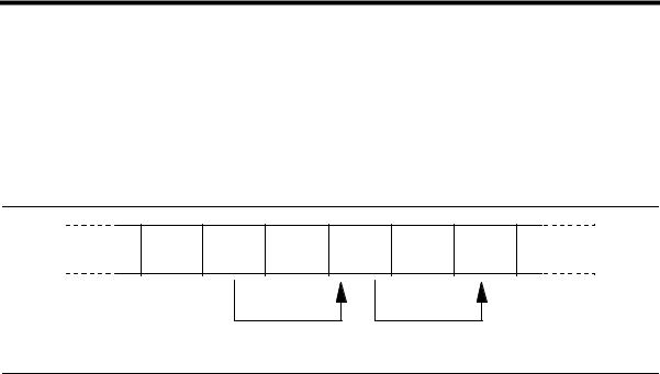
5.0Defect flagging strategy
Media defects are remapped to the next available sector during the Format Process in manufacturing. The mapping from LBA to the physical locations is calculated by an internally maintained table.
Shipped format
•Data areas are optimally used.
•No extra sector is wasted as a spare throughout user data areas.
•All pushes generated by defects are absorbed by the spare tracks of the inner zone.
N N+1 defect N+2 defect N+3
skip skip
Figure 1 PList physical format
Defects are skipped without any constraint, such as track or cylinder boundary. The calculation from LBA to physical is done automatically by internal table. Specification
HITACHI Deskstar & CinemaStar P7K500 Hard Disk Drive specification (Rev 1.1)
14

5.1Electrical interface
5.1.1Connector location
Refer to the following illustration to see the location of the connectors.
PATA MODEL
Figure 2 Connector location (PATA)
SATA MODEL
Figure 3 Connector location (SATA)
HITACHI Deskstar & CinemaStar P7K500 Hard Disk Drive specification (Rev 1.1)
15
5.1.1.14pin DC power connector (only for PATA)
The DC power connector is designed to mate with AMP part number 1-480424-0 using AMP pins part number 350078-4 (strip), part number 61173-4 (loose piece), or their equivalents. Pin assignments are shown in the figure below.
4 |
3 |
2 |
1 |
Pin |
Voltage |
1 |
+12 V |
||||
|
|
|
|
2 |
GND |
|
|
|
|
3 |
GND |
|
|
|
|
4 |
+5V |
Figure 4 Power connector pin assignments
5.1.1.2signal connector
The AT signal connector is a 40-pin connector.
The SATA signal connector is a 8-pin connector. Power connector is a 15-pin connector. (SATA Model)
HITACHI Deskstar & CinemaStar P7K500 Hard Disk Drive specification (Rev 1.1)
16

5.1.2Signal definition(PATA model)
The pin assignments of interface signals are listed in the figure below:
PIN |
SIGNAL |
I/O |
Type |
PIN |
SIGNAL |
I/O |
Type |
01 |
RESET- |
I |
TTL |
02 |
GND |
|
|
03 |
DD7 |
I/O |
3-state |
04 |
DD8 |
I/O |
3-state |
05 |
DD6 |
I/O |
3-state |
06 |
DD9 |
I/O |
3-state |
07 |
DD5 |
I/O |
3-state |
08 |
DD10 |
I/O |
3-state |
09 |
DD4 |
I/O |
3-state |
10 |
DD11 |
I/O |
3-state |
11 |
DD3 |
I/O |
3-state |
12 |
DD12 |
I/O |
3-state |
13 |
DD2 |
I/O |
3-state |
14 |
DD13 |
I/O |
3-state |
15 |
DD1 |
I/O |
3-state |
16 |
DD14 |
I/O |
3-state |
17 |
DD0 |
I/O |
3-state |
18 |
DD15 |
I/O |
3-state |
19 |
GND |
|
|
(20) |
key |
|
|
21 |
DMARQ |
O |
3-state |
22 |
GND |
|
|
23 |
DIOW-(*) |
I |
TTL |
24 |
GND |
|
|
25 |
DIOR-(*) |
I |
TTL |
26 |
GND |
|
|
27 |
IORDY(*) |
O |
3-state |
28 |
CSEL |
I |
TTL |
29 |
DMACK- |
I |
TTL |
30 |
GND |
|
|
31 |
INTRQ |
O |
3-state |
32 |
I |
|
|
33 |
DA1 |
I |
TTL |
34 |
PDIAG- |
I/O |
OC |
35 |
DA0 |
I |
TTL |
36 |
DA2 |
I |
TTL |
37 |
CSO- |
I |
TTL |
38 |
CS1- |
I |
TTL |
39 |
DASP- |
I/O |
OC |
40 |
GND |
|
|
Table 11 Table of signals
Notes:
1."O" designates an output from the drive.
2."I" designates an input to the drive.
3."I/O" designates an input/output common.
4."OC" designates open-collector or open-drain output.
5.The signal lines marked with (*) are redefined during the Ultra DMA protocol to provide special functions. These lines change from the conventional to special definitions at the moment the Host decides to allow a DMA burst if the Ultra DMA transfer mode was previously chosen via SetFeatures. The Drive becomes aware of this change upon assertion of the DMACKline. These lines revert back to their original definitions upon the deassertion of DMACKat the termination of the DMA burst.
|
Special Definition |
Conventional Definition |
|
(for Ultra DMA) |
|
|
|
|
|
DDMARDY- |
IORDY |
Write Operation |
HSTROBE |
DIOR- |
|
STOP |
DIOW- |
Read Operation |
HDMARDY- |
DIOR- |
DSTROBE |
IORDY |
|
|
STOP |
DIOW- |
Table 12 Signal special definitions for Ultra DMA
HITACHI Deskstar & CinemaStar P7K500 Hard Disk Drive specification (Rev 1.1)
17
DD0-DD15 |
16-bit bi-directional data bus between the host and the drive. The lower 8 lines, DD00-07, |
|
are used for Register and ECC access. All 16 lines, DD00-15, are used for data transfer. |
|
These are 3-State lines with 24 mA current sink capability. |
DA0-DA2 |
Address used to select the individual register in the drive. |
CS0- |
Chip select signal generated from the Host address bus. When active, one of the Command |
|
Block Registers (Data, Error {Features when written}, Sector Count, Sector Number, |
|
Cylinder Low, Cylinder High, Drive/Head and Status {Command when written} register) can |
|
be selected. (See Table 26: "I/O address map" on page 34) |
CS1- |
Chip select signal generated from the Host address bus. When active one of the Control |
|
Block Registers (Alternate Status {Device Control when written}) can be selected. (See |
|
Table 26: "I/O address map" on page 34) |
RESET- |
This line is used to reset the drive. It shall be kept in Low logic state during power up and in |
|
High thereafter. |
DIOW- |
Its rising edge holds data from the host data bus to a register or data register of the drive. |
DIOR- |
When low, this signal enables data from a register or data register of the drive onto data bus. |
|
The data on the bus shall be latched on the rising edge of DIOR-. |
INTRQ |
Interrupt is enabled only when the drive is selected and the host activates the nIEN bit in the |
|
Device Control Reg. Otherwise, this signal is in high impedance state regardless of the state |
|
of the IRQ bit. The interrupt is set when the IRQ bit is set by the drive CPU. IRQ is reset to |
|
zero by a host read of the status register or a write to the Command Reg. This signal is a |
|
3-State line with 24 mA sink capability. |
DASP- |
This is a time-multiplexed signal which indicates that a drive is active, or that device 1 is |
|
present. This signal is driven by Open-Drain driver and internally pulled up to 5 volts through |
|
a 10kΩ resistor. |
|
During Power-On initialization or after RESETis negated, DASPshall be asserted by |
|
Device 1 within 400 ms to indicate that device 1 is present. Device 0 shall allow up to 450 |
|
ms for device 1 to assert DASP-. If device 1 is not present, device 0 may assert DASPto |
|
drive a LED indicator. |
|
DASPshall be negated following acceptance of the first valid command by device 1. At |
|
anytime after negation of DASP-, either drive may assert DASPto indicate that a drive is |
|
active. |
PDIAG- |
PDIAGshall be asserted by device 1 to indicate to device 0 that it has completed |
|
diagnostics. This line is pulled-up to 5 volts in the drive through a 10kΩ resistor. |
|
Following a Power On Reset, software reset, or RESET-, drive 1 shall negate PDIAGwithin |
|
1 ms (to indicate to device 0 that it is busy). Drive 1 shall then assert PDIAGwithin 30 |
|
seconds to indicate that it is no longer busy and is able to provide status. |
|
Following the receipt of a valid Execute Drive Diagnostics command, device 1 shall negate |
|
PDIAGwithin 1 ms to indicate to device 0 that it is busy and has not yet passed its drive |
|
diagnostics. If device 1 is present, device 0 shall wait up to 6 seconds from the receipt of a |
|
valid Execute Drive Diagnostics command for drive 1 to assert PDIAG-. Device 1 should |
|
clear BSY before asserting PDIAG-, as PDIAGis used to indicate that device 1 has passed |
|
its diagnostics and is ready to post status. |
|
If device 1 did not assert DASPduring reset initialization, device 0 shall post its own status |
|
immediately after it completes diagnostics and clear the device 1 Status register to 00h. |
|
Device 0 may be unable to accept commands until it has finished its reset procedure and is |
|
ready (DRDY=1). |
|
Device 1 shall release PDIAG-/CBLID- no later than after the first command following a |
|
power on or hardware reset sequence so that the host may sample PDIAG-/CBLID- in order |
|
to detect the presence or absence of an 80-conductor cable assembly. |
HITACHI Deskstar & CinemaStar P7K500 Hard Disk Drive specification (Rev 1.1)
18
CSEL (Cable Select) (Optional)
The drive is configured as either Device 0 or 1 depending upon the value of CSEL.
•If CSEL is grounded, the device address is 0.
•If CSEL is open, the device address is 1.
KEY |
Pin position 20 has no connection pin. It is recommended to close the respective position of |
|
the cable connector in order to avoid incorrect insertion by mistake. |
IORDY |
This signal is negated to extend the host transfer cycle when a drive is not ready to respond |
|
to a data transfer request and may be negated when the host transfer cycle is less than 240 |
|
ns for PIO data transfer. This signal is an open-drain output with 24 mA sink capability and |
|
an external resistor is needed to pull up this line to 5 volts. |
DMACK- |
This signal shall be used by the host in response to DMARQ to either acknowledge that data |
|
has been accepted or that data is available. |
|
This signal is internally pulled up to 3.3 V through a 15 KΩ resistor. The tolerance of the |
|
resistor value is –50% to +100%. |
DMARQ |
This signal, used for DMA data transfers between host and drive, shall be asserted by the |
|
drive when it is ready to transfer data to or from the host. The direction of data transfer is |
|
controlled by DIORand DIOW-. This signal is used on a handshake manner with DMACK-. |
|
This signal is a 3-state line with 24mA sink capability and internally pulled down to GND |
|
through 10 KΩ resistor. |
HDMARDY- (Ultra DMA)
This signal is used only for Ultra DMA data transfers between the host and the device.
HDMARDYis a flow control signal for Ultra DMA data in bursts. This signal is held asserted by the host to indicate to the device that the host is ready to receive Ultra DMA data in transfers. The host may negate HDMARDYto pause an Ultra DMA data in transfer.
HSTROBE (Ultra DMA)
This signal is used only for Ultra DMA data transfers between the host and the device.
HSTROBE is the data out strobe signal from the host for an Ultra DMA data out transfer. Both the rising and falling edge of HSTROBE latch the data from DD(15:0) into the device. The host may stop toggling HSTROBE to pause an Ultra DMA data out transfer.
STOP (Ultra DMA)
This signal is used only for Ultra DMA data transfers between the host and the device.
STOP shall be asserted by the host prior to initiation of an Ultra DMA burst. STOP shall be negated by the host before data is transferred in an Ultra DMA burst. Assertion of STOP by the host during or after data transfer in an Ultra DMA mode signals the termination of the burst.
DDMARDY- (Ultra DMA)
This signal is used only for Ultra DMA data transfers between the host and the device.
DDMARDYis a flow control signal for Ultra DMA data out bursts. This signal is held asserted by the device to indicate to the host that the device is ready to receive Ultra DMA data out transfers. The device may negate DDMARDYto pause an Ultra DMA data out transfer.
DSTROBE (Ultra DMA)
This signal is used only for Ultra DMA data transfers between the host and the device.
DSTROBE is the data in strobe signal from the device for an Ultra DMA data in transfer. Both the rising and falling edge of DSTROBE latch the data from DD(15:0) into the host. The device may stop toggling DSTROBE to pause an Ultra DMA data in transfer.
Device Termination
The termination resistors on the device side are implemented on the drive side as follows:
•33 Ω for DD0 thru DD15, DMARQ, INTRQ
•82 Ω for CS0-, CS1-, DA0, DA1, DA2, DIOR-, DIOW-, DMACK-
•22 Ω for IORDY
HITACHI Deskstar & CinemaStar P7K500 Hard Disk Drive specification (Rev 1.1)
19

5.1.3Interface logic signal levels(PATA model)
The interface logic signal has the following electrical specifications:
Inputs |
Input High Voltage |
2.0 |
V min. |
|
Input Low Voltage |
0.8 |
V max. |
Outputs |
Output High Voltage |
2.4 |
V min. |
|
Output Low Voltage |
0.5 |
V max. |
5.1.4Signal definition(SATA model)
|
|
SATA has receivers and drivers to be connected to Tx+/- and Rx +/- Serial data signal |
defines the |
||||
|
signal names of I/O connector pin and signal name. |
|
|
|
|||
|
|
|
|
|
|
|
|
|
|
No. |
|
Plug Connector pin definition |
Signal |
I/O |
|
|
|
S1 |
GND |
2nd mate |
Gnd |
|
|
|
|
S2 |
A+ |
Differential signal A from Phy |
RX+ |
Input |
|
|
|
S3 |
A- |
|
RX- |
Input |
|
Signal |
|
S4 |
Gnd |
2nd mate |
Gnd |
|
|
|
|
S5 |
B- |
Differential signal B from Phy |
TX- |
Output |
|
|
|
S6 |
B+ |
|
TX+ |
Output |
|
|
|
S7 |
Gnd |
2nd mate |
Gnd |
|
|
|
|
|
|
Key and spacing separate signal and power segments |
|
|
|
|
|
P1 |
V33 |
3.3V power |
3.3V |
|
|
|
|
P2 |
V33 |
3.3V power |
3.3V |
|
|
|
|
P3 |
V33 |
3.3V power, pre-charge, 2nd Mate |
3.3V |
|
|
|
|
P4 |
Gnd |
1st mate |
Gnd |
|
|
|
|
P5 |
Gnd |
2nd mate |
Gnd |
|
|
|
|
P6 |
Gnd |
2nd mate |
Gnd |
|
|
|
|
P7 |
V5 |
5V power,pre-charge,2nd Mate |
5V |
|
|
|
|
P8 |
V5 |
5V power |
5V |
|
|
Power |
|
P9 |
V5 |
5V power |
5V |
|
|
|
|
P10 |
Gnd |
2nd mate |
Gnd |
|
|
|
|
P11 |
Reserved |
Support staggered spin-up and LED activity |
Reserve |
|
|
|
|
P12 |
Gnd |
1st mate |
Gnd |
|
|
|
|
P13 |
V12 |
12V power,pre-chage,2nd mate |
V12 |
|
|
|
|
P14 |
V12 |
12V power |
V12 |
|
|
|
|
P15 |
V12 |
12V power |
V12 |
|
|
Table 13 Interface connector pins and I/O signals
5.1.4.1TX+ / TX-
These signals are the outbound high-speed differential signals that are connected to the serial ATA cable
5.1.4.2RX+ / RX-
These signals are the inbound high-speed differential signals that are connected to the serial ATA cable.
The following standard shall be referenced about signal specifications.
Serial ATA: High Speed Serialized AT Attachment Revision 1.0a 7-January -2003
HITACHI Deskstar & CinemaStar P7K500 Hard Disk Drive specification (Rev 1.1)
20
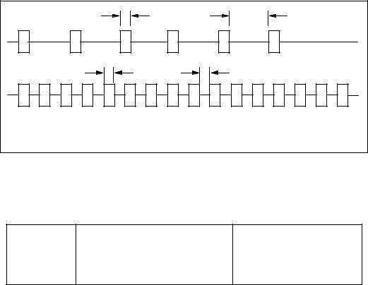
5.1.5Out of band signaling(SATA model)
Figure 5 shows the timing of COMRESET, COMINIT and COMWAKE.
CO M RESET/CO M INIT |
t1 |
t2 |
|
|
|
CO M W AKE |
t3 |
t4 |
Figure 5 the timing of COMRESET, COMINIT and COMWAKE
|
PARAMETER DESCRIPTION |
Nominal (ns) |
t1 |
ALIGN primitives |
106.7 |
t2 |
Spacing |
320 |
t3 |
ALIGN primitives |
106.7 |
t4 |
Psacing |
106.7 |
Table 14 Parameter descriptions
HITACHI Deskstar & CinemaStar P7K500 Hard Disk Drive specification (Rev 1.1)
21
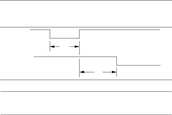
5.2Signal timings
5.2.1Reset timings
Drive reset timing.
RESET-
t10
BUSY
t14
Figure 6 System reset timing chart
|
PARAMETER DESCRIPTION |
Min (usec) |
Max (sec) |
t10 |
RESET low width |
25 |
|
t14 |
RESET high to not BUSY |
– |
31 |
Table 15 System reset timing
HITACHI Deskstar & CinemaStar P7K500 Hard Disk Drive specification (Rev 1.1)
22
 Loading...