


|
|
September 2005 |
|
Training Materials Prepared by: ALVIE RODGERS C.E.T. |
|
|||||||||
|
|
|
|
|
|
|
|
|
|
|
|
|
|
|
|
|
|
|
|
|
|
|
|
|
|
|
|
|
|
|
|
|
|
|
|
|
|
|
|
|
|
|
|
|
|
|
|
|
|
|
|
|
|
|
|
|
|
|
|
|
|
|
|
|
|
|
|
|
|
|
|
|
|
|
|
|
|
|
|
|
|
|
|
|
|
|
|
|
|
|
|
|
|
|
|
|
|
|
|
|
|
|
|
|
|
|
|
|
|
|
|
|
|
|
|
|
|
|
|
2000 MODEL RELEASE
MODEL CHASSIS
53FDX01B DP-05 43FDX01B DP-05F 53SDX01B DP-06 61SDX01B DP-06
DIGITAL
53SWX01W DP-07 61SWX01W DP-07
53SDX88BA DP86V 60SDX88BA DP86V
Updated February 2002
CONTENTS... 2001 DP-0X Chassis Projection Television Information
INSTRUCTOR… Alvie Rodgers C.E.T. (Norcross, GA.)

SEPTEMBER, 2005 |
Table of Contents Page 1 of 4 |
|
|
DP-0X CHASSIS TABLE OF CONTENTS |
|
SECTION (1) GENERAL INFORMATION: |
|
∙ DP-0X FUNCTION Reference Chart --------------------------------------------------------------------------- |
01-01 |
∙ PTV CHASSIS to CHASSIS Cross Reference Chart --------------------------------------------------------- |
01-03 |
∙ PTV CHASSIS to CHASSIS Cross Reference Chart --------------------------------------------------------- |
01-04 |
∙ CTV MODEL to CHASSIS Cross Reference Chart ----------------------------------------------------------- |
01-05 |
∙ CTV CHASSIS to MODEL Cross Reference Chart ----------------------------------------------------------- |
01-06 |
∙ DP-06 and DP-07 REAR PANEL ------------------------------------------------------------------------------- |
01-07 |
∙ DP-05 and DP-05F REAR PANEL ----------------------------------------------------------------------------- |
01-08 |
SECTION (2) MICROPROCESSOR INFORMATION:
∙ |
Microprocessor PORT DESCRIPTION Explanation ------------------------------------------------------- |
02-01 |
∙ Microprocessor PORT DESCRIPTION Circuit Diagram --------------------------------------------------- |
02-10 |
|
∙ DP-05 and 05F Microprocessor PORT DESCRIPTION Explanation ---------------------------------- |
02-11 |
|
∙ DP-05 and 05F Microprocessor PORT DESCRIPTION Circuit Diagram ------------------------------ |
02-12 |
|
∙ |
Microprocessor DATA COMMUNICATION Explanation ------------------------------------------------- |
02-13 |
∙ Microprocessor DATA COMMUNICATION Circuit Diagram--------------------------------------------- |
02-18 |
|
∙ DP-05 and 05F Microprocessor DATA COMMUNICATION Explanation --------------------------- |
02-19 |
|
∙ DP-05 and 05F Microprocessor DATA COMMUNICATION Circuit Diagram ----------------------- |
02-20 |
|
∙ On Screen Display OSD Signal Path Explanation ------------------------------------------------------------- |
02-21 |
|
∙ On Screen Display OSD Signal Path Circuit Diagram--------------------------------------------------------- |
02-23 |
|
∙ Audio and Video MUTE Explanation -------------------------------------------------------------------------- |
02-24 |
|
∙ Audio and Video MUTE Circuit Diagram --------------------------------------------------------------------- |
02-26 |
|
∙ DP-05 and 05F Audio and Video MUTE Explanation ----------------------------------------------------- |
02-27 |
|
∙ DP-05 and 05F Audio and Video MUTE Circuit Diagram ------------------------------------------------ |
02-28 |
|
∙ Mute Circuit SURROUND PWB Explanation ---------------------------------------------------------------- |
02-29 |
|
∙ Mute Circuit SURROUND PWB Circuit Diagram------------------------------------------------------------ |
02-30 |
|
∙ DP-05 and 05F Mute Circuit SURROUND PWB Explanation ------------------------------------------- |
02-31 |
|
∙ DP-05 and 05F Mute Circuit SURROUND PWB Circuit Diagram -------------------------------------- |
02-32 |
|
∙ |
MEMORY INITIALIZATION Explanation ----------------------------------------------------------------- |
02-33 |
∙ EEPROM I2C AVERAGE DATA VALUES ---------------------------------------------------------------- |
02-34 |
|
∙ DAC 1 and 2 Pin Function Explanation ---------------------------------------------------------------------- |
02-37 |
|
SECTION (3) POWER SUPPLY DIAGRAMS: |
|
|
∙ |
POWER ON/OFF Explanation --------------------------------------------------------------------------------- |
03-01 |
∙ POWER ON/OFF Circuit Diagram ---------------------------------------------------------------------------- |
03-04 |
|
∙ Green and Red LED Used for Visual Trouble Shooting Explanation -------------------------------------- |
03-05 |
|
∙ Green and Red LED Used for Visual Trouble Shooting ------------------------------------------------------ |
03-08 |
|
∙ DP-05 and 05F Green and Red LED Used for Visual Trouble Shooting Explanation ----------------- |
03-09 |
|
∙ DP-05 and 05F Green and Red LED Used for Visual Trouble Shooting -------------------------------- |
03-10 |
|
∙ |
|
|
Continued on Next Page

SEPTEMBER, 2005 Table of Contents Page 2 of 4
DP-0X CHASSIS TABLE OF CONTENTS
SECTION (3) POWER SUPPLY DIAGRAMS: (Continued)
∙ Low Voltage Power Supply SHUT DOWN Explanation ---------------------------------------------------- |
03-11 |
|
∙ Low Voltage Power Supply SHUT DOWN Diagram -------------------------------------------------------- |
03-15 |
|
∙ High Voltage Green and Red LED Used for Visual Trouble Shooting Explanation ----------------------- |
03-16 |
|
∙ High Voltage Green and Red LED Used for Visual Trouble Shooting ------------------------------------- |
03-18 |
|
∙ High Voltage Power Supply SHUT DOWN Explanation ---------------------------------------------------- |
03-19 |
|
∙ High Voltage Power Supply SHUT DOWN Diagram -------------------------------------------------------- |
03-24 |
|
SECTION (4) VIDEO CIRCUIT INFORMATION: |
|
|
∙ Model VIDEO Signal Circuit Description ----------------------------------------------------------- |
04-01 |
|
∙ |
Model VIDEO Signal Circuit -------------------------------------------------------------------------- |
04-02 |
∙ |
COMPONENT Circuit Description ------------------------------------------------------------------ |
04-03 |
∙ |
COMPONENT Circuit Diagram ---------------------------------------------------------------------- |
04-04 |
∙ DP-05 and 05F COMPONENT Circuit Description ---------------------------------------------- |
04-05 |
|
∙ DP-05 and 05F COMPONENT Circuit Diagram -------------------------------------------------- |
04-06 |
|
∙ CHROMA After Flex Converter Circuit Description ---------------------------------------------- |
04-07 |
|
∙ CHROMA PHASE ROTATION Circuit Description -------------------------------------------- |
04-08 |
|
∙ CHROMA After Flex Converter Circuit Diagram -------------------------------------------------- |
04-09 |
|
∙ |
SYNC Circuit Description ----------------------------------------------------------------------------- |
04-10 |
∙ |
SYNC Circuit Diagram --------------------------------------------------------------------------------- |
04-11 |
∙ COMPONENT SYNC SEPARATION Circuit Description ------------------------------------- |
04-12 |
|
∙ COMPONENT SYNC SEPARATION Circuit Diagram ----------------------------------------- |
04-13 |
|
∙ DP-05 and 05F COMPONENT SYNC SEPARATION Circuit Description ----------------- |
04-14 |
|
∙ DP-05 and 05F COMPONENT SYNC SEPARATION Circuit Diagram --------------------- |
04-15 |
|
∙ |
Auto Brightness Limiter ABL Description ---------------------------------------------------------- |
04-16 |
∙ Auto Brightness Limiter ABL Circuit ----------------------------------------------------------------- |
04-17 |
|
∙ Horizontal and Vertical SWEEP LOSS Detection Circuit Description -------------------------- |
04-18 |
|
∙ Horizontal and Vertical SWEEP LOSS Detection Circuit ----------------------------------------- |
04-19 |
|
∙ Zenith ZP-04 (Using 3-Line Comb Filter Video Signal Path Description ------------------------ |
04-20 |
|
∙ Zenith ZP-04 (Using 3-Line Comb Filter Video Signal Path -------------------------------------- |
04-21 |
|
SECTION (5) AUDIO CIRCUIT INFORMATION: |
|
|
∙ AUDIO SIGNAL (Main & Terminal) Circuit Description -------------------------------------- |
05-01 |
|
∙ AUDIO SIGNAL (Main & Terminal) Circuit Diagram ------------------------------------------ |
05-02 |
|
∙ AUDIO SURROUND Circuit Description ---------------------------------------------------------- |
05-03 |
|
∙ AUDIO SURROUND Circuit Diagram -------------------------------------------------------------- |
05-04 |
|
∙ DP-05 and 05F CHASSIS SURROUND Circuit Description ------------------------------------ |
05-05 |
|
∙ DP-05 and 05F CHASSIS SURROUND Circuit Diagram --------------------------------------- |
05-06 |
|
Continued on Next Page

SEPTEMBER, 2005 Table of Contents Page 3 of 4
DP-0X CHASSIS TABLE OF CONTENTS
SECTION (6) DIGITAL CONVERGENCE CIRCUIT INFORMATION:
∙ DIGITAL CONVERGENCE Interface Circuit Description -------------------------------------- |
06-01 |
|
∙ DIGITAL CONVERGENCE Interface Circuit Diagram------------------------------------------ |
06-05 |
|
∙ CLU-572 TSI Remote Control used on DP-05, DP-05, DP-06 and DP-07 Chassis ------------ |
06-06 |
|
∙ CLU-573 TSI Remote Control used on AP-93R Chassis ------------------------------------------ |
06-07 |
|
∙ CLU-614 MP Remote Control used on DP-85V Chassis ------------------------------------------ |
06-08 |
|
∙ CLU-436 UII Remote Control used on AP-91 and AP-01 Chassis ------------------------------- |
06-09 |
|
∙ DP-05 and 05F DIGITAL CONVERGENCE Interface Circuit Description ------------------ |
06-10 |
|
∙ DP-05 and 05FF DIGITAL CONVERGENCE Interface Circuit Diagram -------------------- |
06-11 |
|
SECTION (7) DEFLECTION CIRCUIT: |
|
|
∙ DEFLECTION POWER SUPPLY Generation Circuit Description --------------------------- |
07-01 |
|
∙ DEFLECTION POWER SUPPLY Generation Circuit Diagram ------------------------------ |
07-02 |
|
∙ HORIZONTAL DRIVE Circuit Description ------------------------------------------------------- |
07-03 |
|
∙ HORIZONTAL DRIVE Circuit Diagram ---------------------------------------------------------- |
07-05 |
|
∙ HORIZONTAL DRIVE Circuit Diagram ---------------------------------------------------------- |
07-06 |
|
∙ |
DEFLECTION CIRCUIT Block Diagram Explanation ------------------------------------------ |
07-07 |
∙ DEFLECTION CIRCUIT Block Diagram --------------------------------------------------------- |
07-09 |
|
SECTION (8) ADJUSTMENTS: |
|
|
∙ FACTORY RESET PROCEDURE AND CONDITION ------------------------------------------- |
08-01 |
|
∙ |
SIGNAL PWB IDENTIFICATION ------------------------------------------------------------------- |
08-03 |
∙ |
DEFLECTION PWB IDENTIFICATION ----------------------------------------------------------- |
08-04 |
∙ |
CONTROL PWB IDENTIFICATION ---------------------------------------------------------------- |
08-05 |
∙ SUB POWER SUPPLY PWB IDENTIFICATION ------------------------------------------------- |
08-06 |
|
∙ |
CRT PWB IDENTIFICATION ------------------------------------------------------------------------ |
08-07 |
∙ |
CLOCK SPEED ACCELERATION------------------------------------------------------------------- |
08-08 |
∙ |
HIGH VOLTAGE ADJUSTMENT-------------------------------------------------------------------- |
08-09 |
∙ HIGH VOLTAGE LIMITER CIRCUIT CHECK---------------------------------------------------- |
08-10 |
|
∙ FLYBACK PROTECTION CIRCUIT CHECK ----------------------------------------------------- |
08-11 |
|
∙ SWEEP LOSS DETECTION CIRCUIT CHECK --------------------------------------------------- |
08-12 |
|
∙ POWER SUPPLY VOLTAGE CHECK -------------------------------------------------------------- |
08-13 |
|
∙ MAGNET AND YOKE LOCATIONS --------------------------------------------------------------- |
08-14 |
|
∙ |
ADJUSTMENT ORDER ------------------------------------------------------------------------------- |
08-15 |
∙ |
PRE HEAT RUN ---------------------------------------------------------------------------------------- |
08-16 |
∙ |
CUT OFF ADJUSTMENT ----------------------------------------------------------------------------- |
08-17 |
∙ |
PRE-FOCUS ADJUSTMENT ------------------------------------------------------------------------- |
08-18 |
∙ DCU CROSS HATCH PHASE SETTING ----------------------------------------------------------- |
08-19 |
|
∙ HORIZONTAL POSITION (COARSE) ADJUSTMENT ----------------------------------------- |
08-20 |
|
Continued on Next Page

SEPTEMBER, 2005 Table of Contents Page 4 of 4
DP-0X CHASSIS TABLE OF CONTENTS
SECTION (8) ADJUSTMENTS: (Continued)
∙ |
RASTER TILT ------------------------------------------------------------------------------------------- |
08-21 |
∙ |
BEAM ALIGNMENT ---------------------------------------------------------------------------------- |
08-22 |
∙ RASTER POSITION [Off-Set for Red and Blue]---------------------------------------------------- |
08-23 |
|
∙ HORIZONTAL AND VERTICAL SIZE ADJUSTMENT ---------------------------------------- |
08-24 |
|
∙ |
BEAM FORM ADJUSTMENT ----------------------------------------------------------------------- |
08-26 |
∙ |
LENS FOCUS ADJUSTMENT ----------------------------------------------------------------------- |
08-27 |
∙ |
STATIC FOCUS ADJUSTMENT -------------------------------------------------------------------- |
08-28 |
∙ |
BLUE DEFOCUS ADJUSTMENT ------------------------------------------------------------------- |
08-29 |
∙ |
WHITE BALANCE ADJUSTMENT ----------------------------------------------------------------- |
08-30 |
∙ |
SUB BRIGHTNESS ADJUSTMENT ---------------------------------------------------------------- |
08-31 |
∙ HORIZONTAL POSITION (FINE) ADJUSTMENT ----------------------------------------------- |
08-32 |
|
∙ |
OVERLAY DIMENSIONS ---------------------------------------------------------------------------- |
08-33 |
∙ STOPPING POSITIONS IN THE 3X3, 5X7 and 13X9 MODES --------------------------------- |
08-38 |
|
∙ |
DIGITAL CONVERGENCE --------------------------------------------------------------------------- |
08-40 |
SECTION (9) KEY COMPONENTS: |
|
|
∙ DP-06 KEY COMPONENTS ------------------------------------------------------------------------ |
09-01 |
|
|
|
|
|
|
|

!"#"$%&' (#)*$+%,(*#'
 -".,(*#'/'

1010 Page
|
|
|
|
|
|
|
|
|
|
|
|
|
|
|
|
|
|
|
|
|
|
|
|
|
|
|
|
|
|
|
|
|
|
|
|
|
|
|
|
|
|
|
|
|
|
MODEL No |
53SDX88BA |
53SDX01B |
53FDX01B |
43FDX01B |
53SWX01W |
IQ50H95W |
IQ50H94W |
50NHP400 |
|
|
|
|
|
|
|
|
|
|
|
|
|
|
|
|
|
|
|
|
60SDX88BA |
61SDX01B |
|
|
61SWX01W |
IQ60H95W |
IQ60H94W |
60NHP400 |
|
|
|
|
|
CHASSIS |
|
|
|
|
|
|
|
|
|
|
|
|
|
DP86V |
DP06 |
DP05 |
DP05F |
DP07 |
ZP04 (OEM) |
ZP05 (OEM) |
SP05 (OEM) |
|
|
|
|
|
|
Aspect |
|
|
|
|
|
|
|
|
|
|
|
|
|
4X3 |
4X3 |
4X3 |
4X3 |
16 X 9 |
4X3 |
4X3 |
4X3 |
|
|
|
|
|
|
|
|
|
|
|
|
|
|
|
|
|
|
Listening Mod Standard |
|
No |
Yes |
No |
No |
Yes |
No |
No |
No |
|
|
|
|
|
|
|
|
|
|
|
|
|
|
|
|
|
|
Listening Mod Night |
|
No |
Yes |
No |
No |
Yes |
No |
No |
No |
|
|
|
|
|
|
|
|
|
|
|
|
|
|
|
|
|
|
Listening Mod Maximum |
|
No |
Yes |
No |
No |
Yes |
No |
No |
No |
|
|
|
|
|
|
|
|
|
|
|
|
|
|
|
|
|
|
Spk Setup |
Front L-R |
Internal |
No |
Yes |
No |
No |
Yes |
No |
No |
No |
|
|
|
|
|
|
|
|
|
|
|
|
|
|
|
|
|
|
|
wExt Amp wLarge |
No |
Yes |
No |
No |
Yes |
No |
No |
No |
|
|
|
|
|
|
|
|
|
|
|
|
|
|
|
|
|
|
|
wExt Amp wSmall |
No |
Yes |
No |
No |
Yes |
No |
No |
No |
|
|
|
|
|
|
|
|
|
|
|
|
|
|
|
|
|
|
Surround |
|
No |
Yes |
No |
No |
Yes |
No |
No |
No |
|
|
|
|
|
|
|
|
|
|
|
|
|
|
|
|
|
|
Sub Woofer |
|
No |
Yes |
No |
No |
Yes |
No |
No |
No |
|
|
|
Dig Input |
Coaxial |
V1/V2 |
No |
Yes |
No |
No |
Yes |
No |
No |
No |
|
|
|
|
|
|
|
|
|
|
|
|
|
|
|
|
|
|
Optical |
V1/V2 |
No |
Yes |
No |
No |
Yes |
No |
No |
No |
|
|
|
|
|
|
|
|
|
|
|
|
|
|
|
|
|
SRS Mode |
On-Off |
|
No |
No |
Yes |
Yes |
No |
Yes |
Yes |
Yes |
|
|
|
|
|
|
|
|
|
|
|
|
|
|
|
|
|
Graphic EQ 7 band |
|
Yes |
No |
No |
No |
No |
No |
No |
No |
|
|
|
|
|
|
|
|
|
|
|
|
|
|
|
|
|
|
Wireless Sound System |
MainPinPRear |
Yes |
No |
No |
No |
No |
No |
No |
No |
|
|
|
|
|
|
|
|
|
|
|
|
|
|
|
|
|
|
Wireless Sound System |
MainPinP |
No |
No |
No |
No |
No |
No |
No |
No |
|
|
|
|
|
|
|
|
|
|
|
|
|
|
|
|
|
|
Sub Woofer System |
Sub Volume |
Yes |
Yes |
No |
No |
Yes |
No |
No |
No |
|
|
|
|
|
|
|
|
|
|
|
|
|
|
|
|
|
INFORMATION |
Special Event Reminder |
|
Yes |
No |
No |
No |
No |
No |
No |
No |
|
|
|
|
Calendar |
|
|
Yes |
No |
No |
No |
No |
No |
No |
No |
|
|
|
|
|
|
|
|
|
|
|
|
|
|
|
|
|
Auto Help |
|
|
No |
No |
No |
No |
No |
No |
No |
No |
|
|
|
|
|
|
|
|
|
|
|
|
|||
|
GUIDE+ PROGRAM |
GUIDE WITH IR BLASTER |
|
|
|
|
|
|
|
|
|
||
|
OTHERS |
On TV |
Advanced Auto Demo Hold Power |
Yes |
Yes |
Yes |
Yes |
Yes |
Yes |
Yes |
Yes |
|
|
|
|
On TV |
Menu Button |
|
Yes |
Yes |
Yes |
Yes |
Yes |
Yes |
Yes |
Yes |
|
|
|
|
|
|
|
|
|
|
|
|
|
|
|
|
|
On TV |
Cursor Key on Ft Panel |
Yes |
Yes |
Yes |
Yes |
Yes |
Yes |
Yes |
Yes |
|
|
|
|
|
|
|
|
|
|
|
|
|
|
|
|
|
|
On Remote |
Sleep Timer |
|
Yes |
Yes |
Yes |
Yes |
Yes |
Yes |
Yes |
Yes |
|
|
|
|
|
|
|
|
|
|
|
|
|
|
|
|
|
On Remote |
Help |
|
Yes |
Yes |
Yes |
Yes |
Yes |
Yes |
Yes |
Yes |
|
|
|
|
|
|
|
|
|
|
|
|
|
|
|
|
|
On Remote |
Commercial Skip |
Yes |
Yes |
Yes |
Yes |
Yes |
Yes |
Yes |
Yes |
|
|
|
|
|
|
|
|
|
|
|
|
|
|
|
|
|
|
On PinP |
Single PinP Size |
No |
Yes |
Yes |
Yes |
Yes |
Yes |
Yes |
Yes |
|
|
|
|
|
|
|
|
|
|
|
|
|
|
|
|
|
|
On PinP |
Multi PinP 7 Pix |
Yes |
No |
No |
No |
No |
No |
No |
No |
|
|
|
|
|
|
|
|
|
|
|
|
|
|
|
|
|
|
On PinP |
Multi PinP 4 Pix |
No |
No |
No |
No |
No |
No |
No |
No |
|
|
|
|
|
|
|
|
|
|
|
|
|
|
|
|
|
|
On PinP |
Multi PinP 3 Pix |
No |
Yes |
Yes |
Yes |
Yes |
Yes |
Yes |
Yes |
|
|
|
|
On PinP |
Multi PinP Split Screen |
Yes |
Yes |
No |
No |
Yes |
No |
No |
No |
|
|
|
|
|
|
|
|
|
|
|
|
|
|
|
|
|
|
On PinP |
Strobe Action |
|
Yes (7Pix) |
Yes (3Pix) |
Yes (3Pix) |
Yes (3Pix) |
Yes (3Pix) |
Yes (3Pix) |
Yes (3Pix) |
Yes (3Pix) |
|
|
|
|
|
|
|
|
|
|
|
|
|
|
|
|
|
On PinP |
Variable position on Single PinP |
No |
No |
No |
No |
No |
No |
No |
No |
|
|
|
|
|
|
|
|
|
|
|
|
|
|
|
|
|
|
Set Up |
Plug and Play Easy Set Up wColor |
Yes |
Yes |
Yes |
Yes |
Yes |
No |
No |
No |
|
|
|
|
|
|
|
|
|
|
|
|
|
|
|
|
|
|
Set Up |
Auto Clock XDS |
No |
Yes |
Yes |
Yes |
Yes |
Yes |
Yes |
Yes |
|
|
|
|
|
|
|
|
|
|
|
|
|
|
|
|
|
|
Set Up |
Power Resume |
Yes |
Yes |
Yes |
Yes |
Yes |
Yes |
Yes |
Yes |
|
|
|
|
|
|
|
|
|
|
|
|
|
|
|
|
|
|
V Chip |
|
|
Yes |
Yes |
Yes |
Yes |
Yes |
Yes |
Yes |
Yes |
|
|
|
|
|
|
|
|
|
|
|
|
|
|
|
|
|
SP Matrix |
|
|
No |
No |
No |
No |
No |
No |
No |
No |
|
|
|
|
|
|
|
|
|
|
|
|
|
|
|
|
|
Soft Mute |
|
|
Yes |
Yes |
Yes |
Yes |
Yes |
Yes |
Yes |
Yes |
|
|
|
|
|
|
|
|
|
|
|
|
|
|
|
2) of (1 Functions Model 2000

|
|
|
|
|
|
|
|
|
|
|
|
|
|
|
|
|
|
|
|
|
|
|
|
|
|
|
|
|
|
|
|
|
|
MODEL No |
53SDX88BA |
53SDX01B |
53FDX01B |
43FDX01B |
53SWX01W |
IQ50H95W |
IQ50H94W |
50NHP400 |
|
|
|
|
|
|
|
60SDX88BA |
61SDX01B |
|
|
61SWX01W |
IQ60H95W |
IQ60H94W |
60NHP400 |
|
|
|
|
|
|
CHASSIS |
|
|
|
|
|
|
|
|
|
|
|
|
|
|
DP86V |
DP06 |
DP05 |
DP05F |
DP07 |
ZP04 (OEM) |
ZP05 (OEM) |
SP05 (OEM) |
|
|
|
|
|
CONTROL PANEL |
2 Piece |
|
Yes |
Yes |
Yes |
Yes |
Yes |
No |
No |
Yes |
|
|
|
|
|
1 Piece |
|
No |
No |
No |
No |
No |
Yes |
Yes |
No |
|
|
|
|
FRONT PANEL |
|
|
|
|
|
|
|
|
|
|
|
|
|
|
Power |
|
Yes |
Yes |
Yes |
Yes |
Yes |
Yes |
Yes |
Yes |
|
|
|
|
|
|
CH Up |
Cursor Up |
Yes |
Yes |
Yes |
Yes |
Yes |
Yes |
Yes |
Yes |
|
|
|
|
|
CH Down |
Cursor Down |
Yes |
Yes |
Yes |
Yes |
Yes |
Yes |
Yes |
Yes |
|
|
|
|
|
Vol Up |
Cursor Right |
Yes |
Yes |
Yes |
Yes |
Yes |
Yes |
Yes |
Yes |
|
|
|
|
|
Vol Down |
Cursor Left |
Yes |
Yes |
Yes |
Yes |
Yes |
Yes |
Yes |
Yes |
|
|
|
|
|
Input |
Exit |
Yes |
Yes |
Yes |
Yes |
Yes |
Yes |
Yes |
Yes |
|
|
|
|
|
Menu |
|
Yes |
Yes |
Yes |
Yes |
Yes |
Yes |
Yes |
Yes |
|
|
|
|
|
Magic Focus Dig Array Static |
|
Yes M.F. |
Yes M.F. |
Yes (ST) |
Yes (ST) |
Yes M.F. |
Yes (ST) |
Yes (ST) |
Yes (ST) |
|
2000 |
|
|
|
IR Receiver |
|
Yes |
Yes |
Yes |
Yes |
Yes |
Yes |
Yes |
Yes |
|
|
|
|
|
|
|
|
|||||||||
|
|
|
Dimmer Sensor |
|
Yes |
Yes |
Yes |
Yes |
Yes |
Yes |
Yes |
Yes |
|
|
|
|
|
Input 3 |
S Input |
Yes |
Yes |
Yes |
Yes |
Yes |
Yes |
Yes |
Yes |
|
Model |
|
|
|
|
V Input |
Yes |
Yes |
Yes |
Yes |
Yes |
Yes |
Yes |
Yes |
|
|
|
|
|
|
|
|
|||||||||
|
|
|
|
L/Mono Input |
Yes |
Yes |
Yes |
Yes |
Yes |
Yes |
Yes |
Yes |
|
|
|
|
|
|
R Input |
Yes |
Yes |
Yes |
Yes |
Yes |
Yes |
Yes |
Yes |
|
|
|
|
REAR PANEL |
Ant A |
|
Yes |
Yes |
Yes |
Yes |
Yes |
Yes |
Yes |
Yes |
|
Functions |
|
|
|
Ant B |
V Input |
Yes |
Yes |
Yes |
Yes |
Yes |
Yes |
Yes |
Yes |
|
|
|
|
|
|
Yes |
Yes |
Yes |
Yes |
Yes |
Yes |
Yes |
Yes |
|
|
|
|
|
|
To Converter |
|
Yes |
Yes |
Yes |
Yes |
Yes |
Yes |
Yes |
Yes |
|
|
|
|
|
Input 1 |
Component |
No |
Yes |
Yes |
Yes |
Yes |
Yes |
Yes |
Yes |
|
|
|
|
|
|
S Input |
Yes |
Yes |
Yes |
Yes |
Yes |
Yes |
Yes |
Yes |
|
|
|
|
|
|
|
|
|
|
|
|
|
|
|
|
(2 |
|
|
|
|
L/Mono Input |
Yes |
Yes |
Yes |
Yes |
Yes |
Yes |
Yes |
Yes |
|
|
|
|
|
|
|
|
|||||||||
|
|
|
|
R Input |
Yes |
Yes |
Yes |
Yes |
Yes |
Yes |
Yes |
Yes |
|
of |
|
|
|
Input 2 |
Component |
Yes |
Yes |
Yes |
Yes |
Yes |
Yes |
Yes |
Yes |
|
|
|
|
|
|
2) |
||||||||||
|
|
|
|
S Input |
Yes |
Yes |
Yes |
Yes |
Yes |
Yes |
Yes |
Yes |
|
|
|
|
|
|
V Input |
Yes |
Yes |
Yes |
Yes |
Yes |
Yes |
Yes |
Yes |
|
|
|
|
|
|
L/Mono Input |
Yes |
Yes |
Yes |
Yes |
Yes |
Yes |
Yes |
Yes |
|
|
|
|
|
|
R Input |
Yes |
Yes |
Yes |
Yes |
Yes |
Yes |
Yes |
Yes |
|
|
|
|
|
Dig Audio Input Coaxial |
|
|
|
|
|
|
|
|
|
|
|
|
|
|
|
No |
Yes |
No |
No |
Yes |
No |
No |
No |
|
|
|
|
|
|
Dig Audio Input Optical |
|
No |
Yes |
No |
No |
Yes |
No |
No |
No |
|
|
|
|
|
Monitor Out |
S |
Yes |
Yes |
Yes |
Yes |
Yes |
Yes |
Yes |
Yes |
|
|
|
|
|
|
V |
Yes |
Yes |
Yes |
Yes |
Yes |
Yes |
Yes |
Yes |
|
|
|
|
|
|
L |
Yes |
Yes |
Yes |
Yes |
Yes |
Yes |
Yes |
Yes |
|
|
|
|
|
|
R |
Yes |
Yes |
Yes |
Yes |
Yes |
Yes |
Yes |
Yes |
|
|
|
|
|
Audio Hi-Fi Out |
|
|
|
|
|
|
|
|
|
|
|
Page |
|
|
L |
Yes |
Yes |
Yes |
Yes |
Yes |
Yes |
Yes |
Yes |
|
|
|
|
|
|
R |
Yes |
Yes |
Yes |
Yes |
Yes |
Yes |
Yes |
Yes |
|
|
|
|
|
|
|
|
|
|||||||||
01 |
|
|
Wireless Out |
L |
Yes |
No |
No |
No |
No |
No |
No |
No |
|
|
|
|
|
R |
Yes |
No |
No |
No |
No |
No |
No |
No |
|
|
|
20- |
|
|
|
|
|
|||||||||
|
|
Sub Woofer Out |
|
Yes |
Yes |
No |
No |
Yes |
No |
No |
No |
|
|
|
|
|
|
Rear Spk Out |
L |
Yes |
Yes |
No |
No |
Yes |
No |
No |
No |
|
|
|
|
|
|
R |
Yes |
Yes |
No |
No |
Yes |
No |
No |
No |
|
|
PTV MODEL TO CHASSIS CROSS REFERENCE CHART
ModelNo |
Chassis |
|
ModelNo |
Chassis |
|
ModelNo |
Chassis |
43FDX01B |
DP05F |
|
50SX6P |
AP43B |
|
60SX11K |
AP53D |
43GX01B |
AP02 |
|
50UX10B |
AP23 |
|
60SX11KA |
AP53DP |
46EX2B/K |
AP22 |
|
50UX11K |
AP23 |
|
60SX12B |
AP63B |
46EX3B/BS |
AP32 |
|
50UX14B |
AP33 |
|
60SX13K |
AP63B |
46EX4K/KS |
AP32 |
|
50UX15K |
AP33 |
|
60SX1K |
AP14 |
46GX01B |
AP92R |
|
50UX18B |
AP43 |
|
60SX2K |
AP24 |
46UX10BA |
AP13 |
|
50UX19K |
AP43 |
|
60SX3B |
AP34 |
46UX10BF |
AP23 |
|
50UX22B |
AP53 |
|
60SX4K |
AP34 |
46UX11KA |
AP13 |
|
50UX22BA |
AP53P |
|
60SX8B |
AP43B |
46UX11KF |
AP23 |
|
50UX23K |
AP53 |
|
60SX9K |
AP43B |
46UX12B |
AP33 |
|
50UX23KA |
AP53P |
|
60UX54B |
AP73 |
46UX13K |
AP33 |
|
50UX26B |
AP63 |
|
60UX55K |
AP73 |
46UX16B |
AP43 |
|
50UX27K |
AP63 |
|
60UX57B |
AP83R |
46UX17K |
AP43 |
|
50UX52B |
AP73 |
|
60UX58B |
AP83 |
46UX20B |
AP53 |
|
50UX53K |
AP73 |
|
60UX58K |
AP83 |
46UX20BA |
AP53P |
|
50UX57B |
AP83R |
|
60UX59B |
AP93 |
46UX21K |
AP53 |
|
50UX58B |
AP83 |
|
61DMX01W |
NEW |
46UX21KA |
AP53P |
|
50UX58K |
AP83 |
|
61HDX01W |
DP85 |
46UX24B |
AP63 |
|
50UX59B |
AP93 |
|
61HDX98B |
DP85 |
46UX25K |
AP63 |
|
50UX7B/K/W |
AP13 |
|
61SBX01B |
AP93R |
46UX50B |
AP73 |
|
50UX8D/W |
AP13 |
|
61SBX59B |
AP93 |
46UX51K |
AP73 |
|
52LDX99B |
DL1 |
|
61SDX01B |
DP06 |
46UX7B/K |
AP13 |
|
53FDX01B |
DP05 |
|
61SWX01W |
DP07 |
50CX01B |
AP90R |
|
53SBX01B |
AP93R |
|
70SBX74B |
AP74 |
50CX29B |
AP90 |
|
53SBX59B |
AP93 |
|
CT4271 |
VP6 |
50ES1B/K |
AP31 |
|
53SDX01B |
DP06 |
|
CT4275 |
VP6X2 |
50EX01B |
AP91R |
|
53SDX88BA |
DP86V |
|
CT4520K |
VP7X2 |
50EX10B |
AP32 |
|
53SDX89B |
DP86 |
|
CT4521K |
VP7X2 |
50EX11BV |
AP32 |
|
53SWX01W |
DP07 |
|
CT4525 |
VP2 |
50EX12B |
AP32F |
|
55EX15K |
AP52 |
|
CT4531 |
VP2 |
50EX12BA |
AP32V |
|
55EX1K |
AP12 |
|
CT4532 |
VP2 |
50EX12BX |
AP52 |
|
55EX7K |
AP32 |
|
CT4533K |
VP9X1 |
50EX13K |
AP32F |
|
55EX9K |
AP32 |
|
CT4534 |
VP3 |
50EX13KA |
AP32V |
|
55FX20B |
AP62 |
|
CT4535K |
VP9X1 |
50EX13KX |
AP52 |
|
55FX48B |
AP82 |
|
CT4536 |
VP3 |
50EX14BV |
AP52 |
|
55FX49B |
AP92 |
|
CT4546 |
VP3 |
50EX16B |
AP52 |
|
55UX58B |
AP83P |
|
CT4555 |
VP3 |
50EX20B |
AP52 |
|
55UX58BA |
AP83 |
|
CT4580K |
VP7X2 |
50EX2K |
AP22 |
|
55UX59B |
AP93 |
|
CT5033K |
VP9X1 |
50EX39B |
AP91 |
|
60CX01B |
AP90R |
|
CT5071 |
VP6 |
50EX6K |
AP32 |
|
60CX29B |
AP90 |
|
CT5072 |
VP6 |
50EX8K |
AP32 |
|
60EX01B |
AP91R |
|
CT5075 |
VP6X2 |
50FX18B |
AP62 |
|
60EX28B |
AP52P |
|
CT5080 |
VP7X2 |
50FX19K |
AP62 |
|
60EX38B |
AP52P |
|
CT5081K |
VP7X2 |
50FX30B |
AP62 |
|
60EX39B |
AP91 |
|
CT5522K |
VP7X2 |
50FX48B |
AP62P |
|
60FX32B |
AP62 |
|
CT5533K |
VP9X1 |
50FX49B |
AP92 |
|
60GX49B |
AP92 |
|
CT5582K |
VP7X2 |
50GX10B |
AP92R |
|
60SBX72B |
AP74 |
|
CU4600K |
VP8X2 |
50GX20B |
AP92R |
|
60SBX78B |
AP84 |
|
CU4601K |
VP8X2 |
50GX49B |
AP92 |
|
60SDX88B |
DP86 |
|
CU5000K |
VP8X2 |
50SBX70B |
AP74 |
|
60SDX88BA |
DP86V |
|
CU5001B |
VP8X2 |
50SBX78B |
AP84 |
|
60SX10B |
AP53D |
|
CU5002K |
VP8X2 |
50SX5P |
AP33B |
|
60SX10BA |
AP53DP |
|
CU5003D |
VP8X2 |
PAGE 01-03
PTV CHASSIS TO MODEL CROSS REFERENCE CHART
Chassis |
ModelNo |
|
Chassis |
ModelNo |
|
Chassis |
ModelNo |
AP02 |
43GX01B |
|
AP53 |
50UX23K |
|
AP92R |
46GX01B |
AP12 |
55EX1K |
|
AP53D |
60SX10B |
|
AP92R |
50GX10B |
AP13 |
46UX10BA |
|
AP53D |
60SX11K |
|
AP92R |
50GX20B |
AP13 |
46UX11KA |
|
AP53DP |
60SX10BA |
|
AP93 |
50UX59B |
AP13 |
46UX7B/K |
|
AP53DP |
60SX11KA |
|
AP93 |
53SBX59B |
AP13 |
50UX7B/K/W |
|
AP53P |
46UX20BA |
|
AP93 |
55UX59B |
AP13 |
50UX8D/W |
|
AP53P |
46UX21KA |
|
AP93 |
60UX59B |
AP14 |
60SX1K |
|
AP53P |
50UX22BA |
|
AP93 |
61SBX59B |
AP22 |
46EX2B/K |
|
AP53P |
50UX23KA |
|
AP93R |
53SBX01B |
AP22 |
50EX2K |
|
AP62 |
50FX18B |
|
AP93R |
61SBX01B |
AP23 |
46UX10BF |
|
AP62 |
50FX19K |
|
DL1 |
52LDX99B |
AP23 |
46UX11KF |
|
AP62 |
50FX30B |
|
DP05F |
43FDX01B |
AP23 |
50UX10B |
|
AP62 |
55FX20B |
|
DP05 |
53FDX01B |
AP23 |
50UX11K |
|
AP62 |
60FX32B |
|
DP06 |
53SDX01B |
AP24 |
60SX2K |
|
AP62P |
50FX48B |
|
DP06 |
61SDX01B |
AP31 |
50ES1B/K |
|
AP63 |
46UX24B |
|
DP07 |
53SWX01W |
AP32 |
46EX3B/BS |
|
AP63 |
46UX25K |
|
DP07 |
61SWX01W |
AP32 |
46EX4K/KS |
|
AP63 |
50UX26B |
|
DP85 |
61HDX01W |
AP32 |
50EX10B |
|
AP63 |
50UX27K |
|
DP85 |
61HDX98B |
AP32 |
50EX11BV |
|
AP63B |
60SX12B |
|
DP86 |
53SDX89B |
AP32 |
50EX6K |
|
AP63B |
60SX13K |
|
DP86 |
60SDX88B |
AP32 |
50EX8K |
|
AP73 |
46UX50B |
|
DP86V |
53SDX88BA |
AP32 |
55EX7K |
|
AP73 |
46UX51K |
|
DP86V |
60SDX88BA |
AP32 |
55EX9K |
|
AP73 |
50UX52B |
|
NEW |
61DMX01W |
AP32F |
50EX12B |
|
AP73 |
50UX53K |
|
VP2 |
CT4525 |
AP32F |
50EX13K |
|
AP73 |
60UX54B |
|
VP2 |
CT4531 |
AP32V |
50EX12BA |
|
AP73 |
60UX55K |
|
VP2 |
CT4532 |
AP32V |
50EX13KA |
|
AP74 |
50SBX70B |
|
VP3 |
CT4534 |
AP33 |
46UX12B |
|
AP74 |
60SBX72B |
|
VP3 |
CT4536 |
AP33 |
46UX13K |
|
AP74 |
70SBX74B |
|
VP3 |
CT4546 |
AP33 |
50UX14B |
|
AP82 |
55FX48B |
|
VP3 |
CT4555 |
AP33 |
50UX15K |
|
AP83 |
50UX58B |
|
VP6 |
CT4271 |
AP33B |
50SX5P |
|
AP83 |
50UX58K |
|
VP6 |
CT5071 |
AP34 |
60SX3B |
|
AP83 |
55UX58BA |
|
VP6 |
CT5072 |
AP34 |
60SX4K |
|
AP83 |
60UX58B |
|
VP6X2 |
CT4275 |
AP43 |
46UX16B |
|
AP83 |
60UX58K |
|
VP6X2 |
CT5075 |
AP43 |
46UX17K |
|
AP83P |
55UX58B |
|
VP7X2 |
CT4520K |
AP43 |
50UX18B |
|
AP83R |
50UX57B |
|
VP7X2 |
CT4521K |
AP43 |
50UX19K |
|
AP83R |
60UX57B |
|
VP7X2 |
CT4580K |
AP43B |
50SX6P |
|
AP84 |
50SBX78B |
|
VP7X2 |
CT5080 |
AP43B |
60SX8B |
|
AP84 |
60SBX78B |
|
VP7X2 |
CT5081K |
AP43B |
60SX9K |
|
AP90 |
50CX29B |
|
VP7X2 |
CT5522K |
AP52 |
50EX12BX |
|
AP90 |
60CX29B |
|
VP7X2 |
CT5582K |
AP52 |
50EX13KX |
|
AP90R |
50CX01B |
|
VP8X2 |
CU4600K |
AP52 |
50EX14BV |
|
AP90R |
60CX01B |
|
VP8X2 |
CU4601K |
AP52 |
50EX16B |
|
AP91 |
50EX39B |
|
VP8X2 |
CU5000K |
AP52 |
50EX20B |
|
AP91 |
60EX39B |
|
VP8X2 |
CU5001B |
AP52 |
55EX15K |
|
AP91R |
50EX01B |
|
VP8X2 |
CU5002K |
AP52P |
60EX28B |
|
AP91R |
60EX01B |
|
VP8X2 |
CU5003D |
AP52P |
60EX38B |
|
AP92 |
50FX49B |
|
VP9X1 |
CT4533K |
AP53 |
46UX20B |
|
AP92 |
50GX49B |
|
VP9X1 |
CT4535K |
AP53 |
46UX21K |
|
AP92 |
55FX49B |
|
VP9X1 |
CT5033K |
AP53 |
50UX22B |
|
AP92 |
60GX49B |
|
VP9X1 |
CT5533K |
PAGE 01-04
CTV MODEL TO CHASSIS CROSS REFERENCE CHART
ModelNo |
Chassis |
|
ModelNo |
Chassis |
|
ModelNo |
Chassis |
13SA10B |
OEM |
|
31KX41K |
M1CLXU |
|
36SX78B |
M8LXU |
13VR12B |
OEM |
|
31KX6B |
G9LXU1M |
|
36TX53K |
M7LXU |
19VR13B |
OEM |
|
31KX7B |
G9LXU1M |
|
36UX01B |
M10 |
20CX20B |
PANA |
|
31KX9K |
G9LXU1M |
|
36UX52B |
M7LXU |
20MA1B |
FH92XS-1 |
|
31UX5B |
A3LXU |
|
36UX58B |
M7LXU2 |
20SA2B |
M2XU |
|
32CX10B |
A3LXU2 |
|
36UX59B |
M9LXU |
20SA3B |
M3L |
|
32CX11B |
A3LXU3 |
|
CT1386W/B |
G7 |
20SA4B |
M2XU |
|
32CX12B |
A3LXU4 |
|
CT2075W |
G7NU |
20SA5B |
M3XU |
|
32CX32B |
A3LXU3 |
|
CT2076W/B |
G7NU |
27AX0B |
M1LXU |
|
32CX33B |
A3LXU3 |
|
CT2077W/B |
G7XU |
27AX1B |
M1LXU |
|
32CX38B |
A3LXU3 |
|
CT2079B |
G7XU |
27AX2B |
M1LXU |
|
32CX39B |
M9LXU |
|
CT3170 |
G7LXU |
27AX3B |
M1CLXU |
|
32CX39B |
M9LXU |
|
CT3175 |
G7LXU |
27AX4B |
M1CLXU |
|
32CX7B |
A3LXU2 |
|
CT3190B/K |
G9LXU |
27AX5BX |
M1CLXU |
|
32FX41B-501 |
M7LXU |
|
CT3196B/K |
G9LXU |
27CX01B |
SHARP |
|
32FX48B |
M7LXU2 |
|
CT3198K |
G9LXU |
27CX0B |
M1CLXU |
|
32FX49B |
M9LXU |
|
CT7872B/K |
G9LXU |
27CX15B |
M3LXU |
|
32GX01B |
M10 |
|
CT7880 |
G7NU |
27CX1B |
M3LXU |
|
32TX78B |
A3LXU3 |
|
CT7881B/K |
G9LXU |
27CX21B |
M3LXU2 |
|
32TX79K |
A3LXU3 |
|
CT7882B/K |
G9LXU |
27CX22B |
Zenith GX |
|
32UX01B |
M10 |
|
CT7883B |
A1LXU |
27CX25B |
M3LXU |
|
32UX51B |
M7LXU |
|
CT7892B/K |
G9LXU |
27CX28B |
NA6L Pan |
|
32UX58B |
M7LXU2 |
|
CT7893B |
A1LXU |
27CX29B |
OEM |
|
32UX59B |
M9LXU |
|
CT7894B |
A1LXU |
27CX31B |
Zenith GX |
|
32UX8B |
A4LXU |
|
CT7896B |
G9LXU |
27CX3B |
A3LXU |
|
35CX30B |
A3LXU3 |
|
CT7897B |
G9LXU |
27CX4B |
A3LXU |
|
35CX45B |
A3LXU4 |
|
CT7898B |
G9LXU |
27CX5B |
M3LXU |
|
35TX10B |
A3LXU |
|
CT7899K |
G9LXU |
27CX6B |
M3LXU |
|
35TX20B |
A3LXU2 |
|
|
|
27CX75B |
M3LXU2 |
|
35TX30B |
A2LXU |
|
|
|
27CX7B |
M3LXU2 |
|
35TX50B |
A2LXU |
|
|
|
27DX5B |
A1LXU |
|
35TX59K |
A2LXU |
|
|
|
27FX48B |
NA6D Pan |
|
35TX69K |
A2LXU |
|
|
|
27FX90BC |
A2LXU |
|
35TX79K |
A4LXU |
|
|
|
27GX01B |
PANA |
|
35TX88B |
A3LXU3 |
|
|
|
27MM20B |
PA-1 |
|
35TX89K |
A3LXU3 |
|
|
|
27MMV30B |
PA-2 |
|
35UX60B |
A2LXU |
|
|
|
27UX01B |
PANA |
|
35UX70B |
A4LXU |
|
|
|
27UX5B |
A3LXU |
|
35UX70B |
A4LXUP |
|
|
|
31CX4B |
A3LXU |
|
35UX80B |
A4LXUP |
|
|
|
31CX5B |
A3LXU2 1995 |
|
35UX85B |
A6LXU |
|
|
|
31CX5B |
A3LXU2 1996 |
|
36CX35B |
M7LXU |
|
|
|
31CX6B |
A3LXU2 |
|
36FX38B |
M7LXU2 |
|
|
|
31DX10B |
M1LXU1 |
|
36FX42B-501 |
M7LXU |
|
|
|
31DX11B |
M1CLXU |
|
36FX48B |
M7LXU2 |
|
|
|
31DX20B |
M1LXU1 |
|
36FX49B |
M9LXU |
|
|
|
31DX21B |
M1CLXU |
|
36GX01B |
M10 |
|
|
|
31DX22B |
M1CLXU |
|
36MMV60B |
MM1 |
|
|
|
31GX31B |
M1CLXU |
|
36MMV70B |
MM1 |
|
|
|
31KX1B |
G9LXU1M |
|
36SDX01B |
MM-1T |
|
|
|
31KX2B |
G9LXU1M |
|
36SDX01BR |
MM-1R |
|
|
|
31KX39K |
M1CLXU |
|
36SDX88B |
MM1 |
|
|
|
31KX3K |
G9LXU1M |
|
36SX72B |
M8LXU |
|
|
|
PAGE 01-05
CTV CHASSIS TO MODEL CROSS REFERENCE CHART
Chassis |
ModelNo |
|
Chassis |
ModelNo |
|
Chassis |
ModelNo |
A1LXU |
CT7893B |
|
G9LXU |
CT3198K |
|
M7LXU2 |
36FX38B |
A1LXU |
CT7883B |
|
G9LXU |
CT7896B |
|
M8LXU |
36SX72B |
A1LXU |
27DX5B |
|
G9LXU |
CT7892B/K |
|
M8LXU |
36SX78B |
A1LXU |
CT7894B |
|
G9LXU |
CT3196B/K |
|
M9LXU |
36FX49B |
A2LXU |
35TX50B |
|
G9LXU |
CT7881B/K |
|
M9LXU |
36UX59B |
A2LXU |
35UX60B |
|
G9LXU |
CT7882B/K |
|
M9LXU |
32CX39B |
A2LXU |
35TX59K |
|
G9LXU1M |
31KX3K |
|
M9LXU |
32UX59B |
A2LXU |
35TX30B |
|
G9LXU1M |
31KX1B |
|
M9LXU |
32FX49B |
A2LXU |
27FX90BC |
|
G9LXU1M |
31KX2B |
|
M9LXU |
32CX39B |
A2LXU |
35TX69K |
|
G9LXU1M |
31KX6B |
|
MM1 |
36MMV70B |
A3LXU |
27CX3B |
|
G9LXU1M |
31KX7B |
|
MM1 |
36MMV60B |
A3LXU |
35TX10B |
|
G9LXU1M |
31KX9K |
|
MM1 |
36SDX88B |
A3LXU |
27UX5B |
|
M10 |
36UX01B |
|
MM-1R |
36SDX01BR |
A3LXU |
27CX4B |
|
M10 |
32GX01B |
|
MM-1T |
36SDX01B |
A3LXU |
31CX4B |
|
M10 |
36GX01B |
|
NA6D Pan |
27FX48B |
A3LXU |
31UX5B |
|
M10 |
32UX01B |
|
NA6L Pan |
27CX28B |
A3LXU2 |
32CX10B |
|
M1CLXU |
31DX22B |
|
OEM |
13SA10B |
A3LXU2 |
31CX6B |
|
M1CLXU |
27CX0B |
|
OEM |
19VR13B |
A3LXU2 |
35TX20B |
|
M1CLXU |
31DX21B |
|
OEM |
13VR12B |
A3LXU2 |
32CX7B |
|
M1CLXU |
27AX4B |
|
OEM |
27CX29B |
A3LXU2 1995 |
31CX5B |
|
M1CLXU |
31KX39K |
|
PA-1 |
27MM20B |
A3LXU2 1996 |
31CX5B |
|
M1CLXU |
27AX5BX |
|
PA-2 |
27MMV30B |
A3LXU3 |
32TX78B |
|
M1CLXU |
27AX3B |
|
PANA |
27UX01B |
A3LXU3 |
35TX89K |
|
M1CLXU |
31DX11B |
|
PANA |
27GX01B |
A3LXU3 |
35TX88B |
|
M1CLXU |
31GX31B |
|
PANA |
20CX20B |
A3LXU3 |
32TX79K |
|
M1CLXU |
31KX41K |
|
SHARP |
27CX01B |
A3LXU3 |
32CX38B |
|
M1LXU |
27AX0B |
|
Zenith GX |
27CX22B |
A3LXU3 |
32CX33B |
|
M1LXU |
27AX1B |
|
Zenith GX |
27CX31B |
A3LXU3 |
32CX32B |
|
M1LXU |
27AX2B |
|
|
|
A3LXU3 |
32CX11B |
|
M1LXU1 |
31DX20B |
|
|
|
A3LXU3 |
35CX30B |
|
M1LXU1 |
31DX10B |
|
|
|
A3LXU4 |
35CX45B |
|
M2XU |
20SA2B |
|
|
|
A3LXU4 |
32CX12B |
|
M2XU |
20SA4B |
|
|
|
A4LXU |
32UX8B |
|
M3L |
20SA3B |
|
|
|
A4LXU |
35TX79K |
|
M3LXU |
27CX5B |
|
|
|
A4LXU |
35UX70B |
|
M3LXU |
27CX25B |
|
|
|
A4LXUP |
35UX80B |
|
M3LXU |
27CX1B |
|
|
|
A4LXUP |
35UX70B |
|
M3LXU |
27CX15B |
|
|
|
A6LXU |
35UX85B |
|
M3LXU |
27CX6B |
|
|
|
FH92XS-1 |
20MA1B |
|
M3LXU2 |
27CX75B |
|
|
|
G7 |
CT1386W/B |
|
M3LXU2 |
27CX21B |
|
|
|
G7LXU |
CT3170 |
|
M3LXU2 |
27CX7B |
|
|
|
G7LXU |
CT3175 |
|
M3XU |
20SA5B |
|
|
|
G7NU |
CT2075W |
|
M7LXU |
36UX52B |
|
|
|
G7NU |
CT2076W/B |
|
M7LXU |
32UX51B |
|
|
|
G7NU |
CT7880 |
|
M7LXU |
32FX41B-501 |
|
|
|
G7XU |
CT2079B |
|
M7LXU |
36TX53K |
|
|
|
G7XU |
CT2077W/B |
|
M7LXU |
36FX42B-501 |
|
|
|
G9LXU |
CT3190B/K |
|
M7LXU |
36CX35B |
|
|
|
G9LXU |
CT7872B/K |
|
M7LXU2 |
32UX58B |
|
|
|
G9LXU |
CT7898B |
|
M7LXU2 |
36UX58B |
|
|
|
G9LXU |
CT7897B |
|
M7LXU2 |
36FX48B |
|
|
|
G9LXU |
CT7899K |
|
M7LXU2 |
32FX48B |
|
|
|
PAGE 01-06

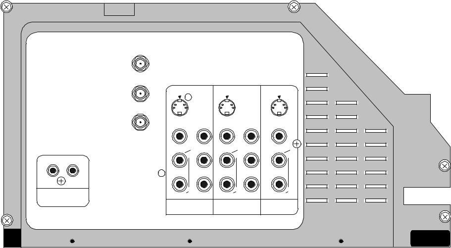
REAR PANEL for the
53SDX01B, 61SBX01B (DP-06) and 61SWX01W, 53SWX01W (DP-07)
OPTICAL
INPUT
COAXIAL
INPUT
REAR SPEAKER  8
8
 ONLY
ONLY
+ 

 +
+
R 


 L
L
- |
- |
R 
 L
L
|
AUDIO |
SUB |
|
TO HI-FI |
WOOFER |
|
|
|
|
|
|
ANT A |
STOP |
|
|
|
CONNECT ONLY 8 Ohm SPEAKERS |
||
|
|
DO NOT SHORT CIRCUIT |
||
To |
|
THESE TERMINALS. |
||
|
(such damage is NOT COVERED |
|||
Converter |
|
by your television warranty) |
||
|
|
|
|
|
S-VIDEO |
|
S-VIDEO |
|
S-VIDEO |
ANT B |
|
|
|
|
VIDEO |
Y |
VIDEO |
Y |
VIDEO |
(MONO) |
PBCB |
(MONO) |
PBCB |
(MONO) |
L |
|
L |
|
|
|
PRCR |
|
PRCR |
|
R |
|
R |
|
R |
AUDIO |
|
AUDIO |
|
AUDIO |
INPUT 1 |
|
INPUT 2 |
|
MONITOR |
|
|
OUT |
||
|
|
|
|
|
07-01 PAGE
REAR PANEL for the 53FDX01B (DP-05) and 43FDX01B (DP05F)
ANT A
To
Converter
ANT B
R L
AUDIO
TO HI-FI
S-VIDEO |
|
S-VIDEO |
|
S-VIDEO |
VIDEO |
Y |
VIDEO |
Y |
VIDEO |
(MONO) |
PBCB |
(MONO) |
PBCB |
(MONO) |
L |
|
L |
|
|
|
PRCR |
|
PRCR |
|
R |
|
R |
|
R |
AUDIO |
|
AUDIO |
|
AUDIO |
INPUT 1 |
|
INPUT 2 |
|
MONITOR |
|
|
OUT |
||
|
|
|
|
08-01 PAGE

MICROPROCESSOR
INFORMATION
 SECTION 2

MICROPROCESSOR PORT DESCRIPTION
DP-0X MICROPROCESSOR PORT DESCRIPTION EXPLANATION:
The DP-0X Microprocessor is a Dual In-Line 64 pin chip. Generic number is MN102H51K. The Microprocessor is responsible for many different operations related to the control of the Projection Television. Some of these controls are automatic and some require customer intervention, either by the Remote control or front panel keys and/ or by the customer’s menu.
When power is first applied, the Microprocessor receives it’s B+. This Microprocessor utilizes a 3.3V power supply instead of the usual 5V as in past chassis.
As the 3.3V is rising, the Reset IC (I006) holds the reset pin (54) low long enough for the main B+ to stabilize. After stabilization, the Reset IC brings pin (54) high. During the Reset condition, the Microprocessor is initiated into its start up state. At the same time this is happening, the Microprocessor Oscillator is generating the Microprocessor’s internal clock. The Crystal responsible for this is X001 (4Mhz) connected to pins (52 and 53). When trouble shooting a Microprocessor for problems, it’s very important to remember the sequence described above. Always examine the process before looking for any other problem area. The order is;
1.Vcc Applied. Generated from the Always Voltage (STY+7V I905) on the Sub Power Supply then through the (STBY +5V I008 on the Signal PWB) to the 3.3V regulator Q026.
2.Ground is available. Look for open traces, etc….
3.The Reset circuit is working (I006). It should hold the Reset pin on the Microprocessor Low until main Vcc is stabilized.
4.The Oscillator is running. Be careful here because a low resistance measuring probe will kill the Oscillator or give a false reading.
After checking for the preliminary functionality of the circuits described above, then check for active clock pulses leaving data port pins. (See the Data Communications Circuit Diagram for details). If some other IC is grounding the data or clock pins, the Microprocessor will not work. This usually require a Pull-Up resistor. If no Pull-Up resistor is noted in the schematic, then the responsibility for Pull-Up lies within the Microprocessor. Unloading the pin in a good way to investigate for Pull-Up.
When a command is entered by either Remote Control, Front Keys or some internal process, the Microprocessor runs a set of predetermined routines. These routines are hard programmed into the Microprocessor RAM and are unchangeable. There are routine instructions that can be modified by either the customer or the Servicer and involve pre-programmed routines and variables entered by the customer or technician. These would include such things as changing the channel , audio set-ups, on/off timer, auto-link, etc...
CONTROL OF THE PROJECTION TELEVISION:
∙Receiving Infrared Remote Control Commands
∙Receiving Key Input Commands
∙Controlling the On and Off state of the High Voltage Power Supply.
∙Interaction between the Customer’s Menu and Chassis controls.
∙Outputting On Screen Display information.
∙Interaction between the Servicer’s Menu and Chassis I2C Data Bus controls.
∙Automatically Scanning the Tuner’s searching for Active Channels when requested by the Customer from the Menu.
∙Automatically Controlling the Tuners when Channels are changed for the Main and PinP Tuners.
∙Automatically Controlling the Video Processor (Rainforest IC) when directed by the Customer.
∙Controlling the Audio Circuits when directed by the Customer.
∙Controlling Switching between Tuner (Main), AVX 1, 2, 3 and 4, Component 1, 2, and Tuner 2 (AUX) or In From Converter.
The following section will explain the controls listed above.
Continued on Next Page
PAGE 02-01

MICROPROCESSOR PORT DESCRIPTION
Continued from Preceding Page
Receiving Infrared Remote Control Commands:
Whenever the Customer utilizes the Infrared Remote, the IR receiver will detect these 38Khz Infrared pulse train and amplify them. These pulses are delivered to the Microprocessor at Pin (1). The Microprocessor decodes this data train and sets off the internal routine related to the command.
There is a time when the Microprocessor ignores the remote commands and that is when the Digital Convergence Unit, (DCU here after) is in operation. The Microprocessor receives a BUSY notification that the DCU is in operation and simply doesn’t respond to remote commands. (See the Digital Convergence Interconnect Diagram and explanation for complete details.) The BUSY signal is generated from the DCU at pin (10). Then out pin (1) of the PSD1 connector to pin (10) of I004 DAC2. I004 sends the information via SCL1 and SDA1 lines from Pin (14 and 15) to the Microprocessor pins (2 and 3).
Receiving Key Input Commands:
The front panel function keys are detected by the Microprocessor via R2 ladder style circuit. In other words, inside the microprocessor is a group of comparators. The function keys are strung together and each one has a different resistor value to ground. When the key is pressed, the comparators detect the change is resistance to ground at pin (20) Clock and convert the related DC value into data the Microprocessor can understand.
The following shows the resistor value to ground from pin (20) of the Microprocessor, though pin (7) of the PFS connector to the individual keys.
Channel Up = ground Channel Down = 1K
Volume Up = 1K + 1.5K or 2.5K
Volume Down = 1K + 1.5K + 2.7K or 5.2K AVX = 1K + 1.5K + 2.7K + 4.7K or 9.9K
Menu = 1K + 1.5K + 2.7K + 4.7K + 10+ or 19.9K
Controlling the On and Off state of the High Voltage Power Supply.
The Power On/Off function switch has STBY+3.3V applied for the Sub Power Supply, via pin (8) of the PFS connector through a 1K resistor. The output of the Power On/Off switch is sent through pin (6) of the PFS to Q014. Q014 is turned on at this time and connected to it’s Emitter is Data from the Microprocessor pin (21). The Data is routed from Q014’s Collector to Key In pin (10) of the Microprocessor. When the Microprocessor receives this data at pin (10), it knows to turn on or off the television. This function is performed by and output from pin (53) which controls Q002. This output from this pin is High when the set is On and Low when the set is Off.
(For more details related to Power On/Off, see the Power On & Off Circuit Diagram Explanation and Diagram).
Interaction between the Customer’s Menu and Chassis controls.
When the Customer accesses the Main Menu, selections can be made by scrolling up and down or left to right. Each selected input activates a set of instructions within the Microprocessor and determines the output state of the related pins.
Outputting On Screen Display information.
When it’s necessary, the Microprocessor generates 1uSec pulses from pins (37 Red, 38 Green and 39 Blue) that are sent to the Rainforest IC (IX01) pins (37 Blue, 38 Green and 39 Red) as OSD signals. When the OSD signals are high, they turn on the output of the Red or Green or Blue amps inside the Rainforest IC and output a pulse to the CRTs to generate that particular character in the particular color.
(See the On Screen Display Circuit Diagram and Explanation for further details.)
(Continued on page 3)
PAGE 02-02
MICROPROCESSOR PORT DESCRIPTION
(Continued from page 2)
Interaction between the Servicer’s Menu and Chassis I2C Data Bus controls.
When it becomes necessary for the Service Technician to make an adjustment to the set, the Service Menu must be entered. This is accomplished with the TV turned off, then by pressing and holding the INPUT Key and then the POWER SWITCH. The Adjustment Menu will be displayed at this time. With the Service Menu activated, the Technician moves up and down to the desired adjustment using the Remote control or front panel Up or Down cursor keys. To make the adjustment, the Technician uses the Remote control or front panel Left and Right cursor Keys to change the data values for the particular adjustment.
The Microprocessor controls the individual IC related to the adjustment using I2C technology. I2C technology allows the Microprocessor to control and IC using only two pins, (SCL and SDA).
The following pins on the Microprocessor and the ICs that it controls are described in the following table.
PINS |
CONTROLLED ICs |
|
|
2 SDA1 and 3 SCL1 |
I401 AV Selector, I002 EEPROM, I003 DAC 1, I004 DAC 2 |
|
|
59 SDA2 and 60 SCL2 |
U204 3D/YC, I701 Deflection Drive, IX01 Rainforest, |
|
IS03 Front Audio Control, IS05 Front EQ, IS10 Center EQ, IS08 Center/LFE/ |
|
PinP Audio Control, IS01 DAC3, I201 1H Main Video, and I403 H Sub Video. |
|
|
57 SDA3 and 58 SCL3 |
IS11 Rear Audio Control. |
|
|
(See the Adjustment Section for actual adjustment made in the Service Mode condition).
Automatically Scanning the Tuner’s searching for Active Channels when requested by the Customer from the Menu.
When the Projection is first installed, the active channels must be scanned and memorized in the Channel Scan List. This list is actually stored within the EEPROM and the Microprocessor uses the information to Scan up or down. Held within the Microprocessor is the Initial FCC Lookup table. This table give information related to all the channels frequency, band, and channel number. The frequency is actually a given value for the Phase Lock Loop circuit within the tuner. Then band is data to tell the band selection circuit in the tuner where the particular channel is located and the channel number is given to the microprocessor to indicate what OSD outputs to produce. When the set is first opened, it’s in what is called Factory Reset Condition. For the Tuner this means that the signal source is AIR, and channels 2 through 13 are in the channel scan list. Before the customer runs Auto Program, they must set the signal source to the type they are using, Air, Cable 1 or Cable 2. After the source is set, the customer then proceeds with Auto Programming.
When Auto Programming is initiated, the Microprocessor has a specific program to run. This program starts by placing the tuner in the lowest channel in the lowest band. That would normally be channel 2. Then the program instruct the Microprocessor to look for Sync. To do this, the Microprocessor actually need Horizontal Blanking (H.Blk) at pin (49) which is labeled H.Sync and Video Sync (24) labeled Main/Sub SD Det.
Horizontal Blanking is use as a gate pulse for the coincidence detector. Within the coincidence detector is a circuit that looks at the timing of the Sync in relationship to (H.BLK). If the signal being checked is not in time with (H.Blk). The signal is ignored. However, if the signal being monitored is in coincidence with (H.Blk) the signal is deemed to be true Video Sync and that particular channel is stored as an active channel in the EEPROM Scan List.
Then the Microprocessor sends information to the tuner to move up one channel and the whole process begins again. This is repeated until every channel is checked. After completion of the scan, the microprocessor retrieves information from the EEPROM concerning the first channel in the lowest band that appears in the scan list and directs the tuner to tune to that channel.
(Continued on page 4)
PAGE 02-03
MICROPROCESSOR PORT DESCRIPTION
(Continued from page 3)
Automatically Controlling the Tuners when Channels are changed. (See Figure 1)
MAIN TUNER:
When channels are changed, the Microprocessor runs another routine. This routine detects the command if it’s input by the Remote Control or the Front keys, whether it’s Scan Up/Down or direct access, and begins to control the Tuner. First the Microprocessor output a Mute command to blank the video, then data is sent to the tuner to move it to the desired channel. After that the Microprocessor again checks the coincidence detector for active sync. If active sync is detected, the Microprocessor opens what is called the AFC Loop. The AFC Loops comprises two cycles trying to lock the tuner to the specific IF frequency of 45.5 Mhz. A DC voltage is sent from either the Main Tuner U201 pin (10) or the PinP Tuner U202 pin (21) back to the Microprocessor pin (6). This DC voltage indicates the error between the IF detected and the IF frequency reference. This error voltage tells the Microprocessor to do one of two things. 1st, if the error is large, the Microprocessor changes the Programmable Divider’s division rate to a larger or smaller degree to get closer to the actual IF frequency desired. Or 2nd move the Pulse Swallow division rate to either 1/32 or 1/33. The Pulse Swallow tuning circuit is a second divider that is on the output from the Prescaler. The main Prescaler takes the very high frequency output from the tuners mixer circuit which is produced when the tuners main oscillator is beat against the incoming RF frequency. The Programmable Divider is instructed by the Microprocessor exactly what division rate to apply to the Beat Frequency generating the IF frequency. The IF frequency is then sent through the Pulse Swallow circuit which again divides the IF frequency at a much smaller rate . This allows the IF output frequency to become much more finite and can correct for much smaller errors between the Phase comparators reference frequency. The error voltage generated is directed back to the main internal Oscillator in the front end and corrects for Tuning errors.
(See the Microprocessor Data Communications Circuit Diagram Explanation for Details related to Data Communication for controlling the Main Tuner).
INTEGRATED TUNER
BM (B+ Mains) |
IF Out |
IF In |
|
|
B+ Distribution |
|
|
Video Det |
Video |
||
|
Pre- |
Programm- |
|
Pulse |
|
5K |
|
|
|
|
Ref |
||||
|
Swallow |
Phase |
|||||
RF |
Scaller |
able |
|||||
1/32 or |
Comparator |
Osc |
|||||
Mix |
Fixed |
Divider |
|||||
|
1/33 |
|
|
||||
Band |
|
|
|
|
|
||
|
|
|
|
|
|
||
Tuning |
|
|
|
|
Error |
|
|
Voltage |
|
|
|
|
|
||
|
|
|
|
Amp |
|
||
|
|
|
|
|
|
||
|
|
|
|
|
IF |
|
|
Main |
|
|
|
|
Comparator |
|
|
|
|
|
|
|
|
||
Osc |
|
|
|
|
|
|
|
|
|
Interface |
|
|
Ref |
|
|
|
|
|
|
Freq. |
|
||
|
|
|
|
|
|
||
|
|
|
|
|
45.5K |
|
|
|
|
Data |
Clock |
Load |
AFC |
|
|
Tuning |
|
|
|
MAIN |
|
Figure 1 |
|
Voltage |
|
|
|
|
|||
|
MICROPROCESSOR |
||||||
+33V |
|
|
|||||
|
|
|
|
|
|
||
(Continued on page 5)
PAGE 02-04
MICROPROCESSOR PORT DESCRIPTION
(Continued from page 4)
Automatically Controlling the Tuners when Channels are changed. (See Figure 1)
PinP TUNER:
As far as the internal function of the PinP Tuner, it is the same as the Main Tuner.
(See the Microprocessor Data Communications Circuit Diagram Explanation for Details related to Data Communication for controlling the Main Tuner).
When the customer presses the PinP button on the Remote Control, the Microprocessor outputs Clock, Data and Enable controls to the Flex Converter. The Flex Converter also has the PinP circuit inside. The Clock, Data and Enable pins on the Microprocessor are pins (20 Clock, 21 Data and 46 FCENABLE) These are routed to the Level Shift IC, I014 pins (2, 3 and 4). They are output on pins (18, 17 and 16) to the Flex Converter U205 connector PFC1 and input on pins (10, 11 and 12). The Flex Converter’s PinP unit is then switched on and insertion is made into the regular Main Video line. The position of the PinP window, the PinP window itself and other different display conditions are controlled by this process. When SWAP is pressed on the remote control, the channel or input that the PinP tuner was on, now becomes the Main Video’s source and the channel or input that the Main signal was on, now becomes the PinP source.
Automatically Controlling the Video Processor (Rainforest IC) when directed by the Customer.
The Rainforest IC has many enhancement circuits built in. These would include the Black Peak Expansion circuit, the Dynamic Noise Reduction circuit, Time Compression and of course Sharpness, Black Level and Contrast adjustments as well.
∙Black Peak Expansion Circuit:
This circuit is utilized to increase the contrast ratio. The standard video signal is 1 Volt Peak to Peak (p/p hear after), the actual video (Y) content is 730mVp/p. The 1 Vp/p is explained it IRE figures from this point on. The Standard video signal is divided into units called IRE. The units are equal to 140 total for the 1Vp/p signal. Sync occupies 40IRE which are negative. And the Luminance represents 100 IRE units. Each unit represents 7.1428mVp/p of information. (See Figure 2 below.)
The Black Peak Expansion circuit monitors the 1/2 way point of luminance, (50 IRE or 357mV) and pulls the signal towards pure black or the 7.5 IRE level. This increases the distance from Black Peak to White Peak which is contrast.
∙Dynamic Noise Reduction Circuit:
This circuit again monitors the area from 50 IRE down and subtracts noise. This circuit is dynamic meaning that it characteristics change. In other words, the subtraction process is greater near black level that it is near 50 IRE. The subtraction is 6dB at maximum, meaning that there would be some frequency loss near black, but the noise which is seen as white speckles would be reduced.
∙Time Compression Circuit:
Any time an analog signal is passed through a capacitive circuit, its high frequencies are reduced. To replace these high frequencies, Hitachi uses Time Compression. This circuit is on the order of Aperture Compensation, however it differs in the fact that it uses 5 delay lines. The actual signal should look like
Figure 2
(Continued on page 6)
PAGE 02-05

MICROPROCESSOR PORT DESCRIPTION
(Continued from page 5)
Figure 3, however after passing through a capacitive circuit, it looks like Figure 4. After Time Compression takes place, the beginning rise is advanced. Just before white peak the signal is delayed. Just before the signal falls the signal is advanced and just before the signal reaches black peak the signal is delayed. This causes the signal to appear more like the actual signal and thus restores the high frequencies lost through capacitance.
Actual Signal |
After passing through a capacitor |
After Time Compression |
||||||||||||||||
|
|
|
|
|
|
|
|
|
|
|
||||||||
|
|
|
|
|
|
|
|
|
|
|
|
|
|
|
|
|
|
|
|
|
|
|
|
|
|
|
|
|
|
|
|
|
|
|
|
|
|
|
|
|
|
|
|
|
|
|
|
|
|
|
|
|
|
|
|
|
|
|
|
|
|
|
|
|
|
|
|
|
|
|
|
|
|
|
|
|
|
|
|
|
|
|
|
|
|
|
|
|
|
|
|
|
|
|
Figure 3 |
Figure 4 |
Figure 5 |
|
|
∙Sharpness:
During the Time Compression process, switching pulses that are detected at the transition point, (A transition is the point at which the luminance signal goes for black to white or white to black) are used in the sharpness circuit.. This signal is the routed through a sort of variable resistor and according to how much sharpness the customer has selected, determines how much of the transition signal is added to the original signal. The greater the sharpness setting, the greater the transition signal added.
Original Signal |
Transition Point pulses |
Transition Pulses Added |
|
Figure 6 |
Figure 7 |
Figure 8 |
|
|
Controlling the Audio Circuits when directed by the Customer.
The customer has control over how the set accesses audio information for all of it’s inputs. The tuner for example is an integrated type. This not only means that held within the Main Tuner are all the necessary components for Reception and Video detection. It also has a built in audio and MTS decoder. The Main Tuner outputs Left Total and Right Total signals. (Left Total and Right Total means that the encoding for Pro-Logic is held within the individual signal.) The customer can select first of all, how the Tuner decodes it’s audio. Stereo, Mono, or SAP can be selected. The Main Tuner must tell the Microprocessor what signal it is receiving. The Main Tuner has a ST LED output at pin (19) which tells the Microprocessor it is receiving MTS Stereo and a SAP LED output at pin (20) which tells the Microprocessor it is receiving Second Audio Program. How these are selected by the consumer via the Main Menu determines the output from the Microprocessor.
∙ST LED is routed from the Main Tuner at pin (19), through Q204, to the DAC1 I003 pin (10). The DAC1 outputs Clock and Data via pins 15 SCL1 and 14 SDA1 signals to the Microprocessor input on pins 3 SCL1 and 2 SDA2. The Microprocessor knows how to switch the tuners decoder circuit by making judgment upon these inputs. Then the Microprocessor can use Clock, Data and Enable lines to control the Tuner.
(Continued on page 7)
PAGE 02-06

MICROPROCESSOR PORT DESCRIPTION
(Continued from page 6)
∙SAP LED is routed from the Main Tuner at pin (20), through Q203, to the DAC1 I003 pin (9). The DAC1 outputs Clock and Data via pins 15 SCL1 and 14 SDA1 signals to the Microprocessor input on pins 3 SCL1 and 2 SDA2.
The Microprocessor knows how to switch the tuners decoder circuit by making judgment upon these inputs. Then the Microprocessor can us Clock, Data and Enable lines to control the Tuner.
Clock, Data and Enable lines for the Main Tuner are output from the Microprocessor at pins (20, 21 and 44) respectively. Pin (44) FEENABLE1 goes directly to the Main Tuner at pin (6), where as the Clock and Data lines must be routed through the Level Shift IC I014 to be brought up to 5V. Clock and Data arrive at I014 at pins (2 and 3) and are output at pins (18 and 17). They arrive at the Main Tuner at pins (4 and 5).
The PinP Tuner doesn’t have MTS capability. It only output mono audio, so no switching takes place for the PinP Tuner U202 audio circuit. The only difference for the PinP tuner control lines is related to the PinP Enable line. This is output from the Microprocessor pin (43 FEENABLE2) to the PinP Tuner at pin (17). Clock and Data are the same as for the Main Tuner.
(See Microprocessor Data Communications Circuit Diagram and Explanation for further details).
Controlling Switching between Tuner (Main), AVX 1, 2, 3 and 4, Component 1, and 2, and Tuner 2 (AUX) or In From Converter.
The different inputs can be selected by the Remote Control or the Front Panel switches. This is accomplished by the INPUT button. Each time the Input button is pressed, the different inputs are sequentially selected. The sequential order is, Main Tuner, AVX 1, AVX 2, AVX 3, AVX 4, 2nd Antenna and back to Main Tuner. Also, if there are S-Inputs on AVX1, 2 or 4, there is an internal mechanical switch inside the S-Jack that tells the Microprocessor an S-Jack is inserted. Then when that particular input is selected, it automatically selects S as it’s source. The same thing holds true for Component inputs. The set should never have Component inputs and S-Jack inserted at the same time and a black and white picture will be displayed.
(See Video Signal Processing for details related to Video Switching.)
PAGE 02-07
|
|
|
|
|
|
|
|
|
|
|
|
|
|
|
|
|
|
|
DP-0X CHASSIS MICROPROCESSOR I-001 PIN/PORT DESCRIPTION 1 through 35 |
|
|
||
|
|
|
Pin No. |
ID |
Function |
Active |
|
|
|
|
1 |
IRIN |
Receives Remote Control Inferred pulses. |
Data |
|
|
|
|
|
|
|
|
|
|
|
|
2 |
SDA1 |
Serial Data Sent and Received from the EEPROM, A/V Selector, DAC1, DAC2. Function of I2C. |
Data |
|
|
|
|
3 |
SCL1 |
Serial Clock Synchronization Sent to the EEPROM, A/V Selector, DAC1, DAC2. Function of I2C. |
Data |
|
|
|
|
4 |
Dimmer |
Receives DC voltage generated from the Photo Receiver on the Front Panel monitoring Room Light. For AI |
DC |
|
|
|
|
|
|
|
|
|
|
|
|
5 |
AD Key In |
Receives Level Shifted DC voltage from Front Panel Key presses. |
DC |
|
|
|
|
|
|
|
|
|
|
|
|
6 |
Main/Sub AFC |
Receives the Main Tuner AFC or Sub AFC DC Voltage switched by I005. Used during channel change. |
DC |
|
|
|
|
|
|
|
|
|
|
|
|
7 |
Key In |
When the Power switch is pressed, Clock data from pin 21 is routed through Q014 back to this pin. Power is toggled On or Off. |
Data |
|
|
|
|
|
|
|
|
|
|
|
|
8 |
Not Used |
Not Used |
N/A |
|
|
|
|
|
|
|
|
|
|
|
|
9 |
Not Used |
Not Used |
N/A |
|
|
|
|
|
|
|
|
|
|
|
|
10 |
Main FV Det |
Receives Composite 1 V Sync from I015 pin 4 for OSD Positioning. |
Sync |
|
|
|
|
|
|
|
|
|
|
|
|
11 |
Sub FV Det |
Receives Composite 2 V Sync from I016 pin 4 for OSD Positioning. |
Sync |
|
|
|
|
|
|
|
|
|
|
|
|
12 |
DSP Busy |
Receives the Busy command from the Digital Surround Processor on the Surround PWB. |
DC |
|
|
|
|
|
|
|
|
|
|
|
|
13 |
DSP SO |
Control command to the DSP Unit for controlling Modes. |
Data |
|
|
|
|
|
|
|
|
|
|
|
|
14 |
DSP Dir |
Receives Digital Surround Processor Error information from the DSP unit on the Surround PWB. |
Data |
|
|
|
|
|
|
|
|
|
|
|
|
15 |
DSP SS |
Control command to the DSP Unit for controlling Modes. |
Data |
|
|
|
|
|
|
|
|
|
|
|
|
16 |
DSP SCK |
Digital Surround Processor Clock. |
Data |
|
|
|
|
|
|
|
|
|
|
|
|
17 |
DSP S1 |
Control command to the DSP Unit for controlling Modes. |
Data |
|
|
|
|
|
|
|
|
|
|
|
|
18 |
DSP ERR Mute |
Mutes Audio when a DSP Dir input is detected. (DSP Error). |
DC High |
|
|
|
|
|
|
|
|
|
|
|
|
19 |
DSP Reset |
Resets the DSP module on the Surround PWB |
DC High |
|
|
|
|
|
|
|
|
|
|
|
|
20 |
Clock |
Sent to the Level Shift I014 then to both Tuners and the Flex Converter as a timing signal. Also see pin 7. |
Data |
|
|
|
|
|
|
|
|
|
|
|
|
21 |
Data |
Sent to the Level Shift I014 then to both Tuners and the Flex Converter to control each unit. |
Data |
|
|
|
|
|
|
|
|
|
|
|
|
22 |
Comp 1/2 FH Det |
Either Component One or Two Horizontal Input from I005 through Q046. Used for OSD Display. And Auto Link |
DC |
|
|
|
|
|
|
|
|
|
|
|
|
23 |
AC In |
Receives Timing pulses for advancing the Clock. Received from the Smitt Amp Q008 and Q009 |
60Hz. |
|
|
|
|
|
|
|
|
|
|
|
|
24 |
Main/Sub SD Det |
Station Detection. Used during Auto Programming and when channels are changed to open AFC Loop. Switched by I005. |
Sync |
|
|
|
|
|
|
|
|
|
|
|
|
25 |
VDD |
Stby +3.3V generated by 0029. Main Microprocessor B+. |
DC |
|
|
|
|
|
|
|
|
|
|
|
|
26 |
CHL |
Clamp level High |
DC |
|
|
|
|
|
|
|
|
|
|
|
|
27 |
VRefFHS |
Use as a reference signal within the Microprocessor High Frequencies. |
DC |
|
|
|
|
|
|
|
|
|
|
|
|
28 |
CVBS0 |
Composite Sync used for Closed Caption Detection for the Main Tuner. |
Sync |
|
|
|
|
|
|
|
|
|
|
|
|
29 |
VSS |
Ground |
N/A |
|
|
|
|
|
|
|
|
|
|
|
|
30 |
CVBS1 |
Not Used. Composite Sync used for Closed Caption Detection for the PinP Tuner. |
N/A |
|
|
|
|
|
|
|
|
|
|
|
|
31 |
VREFLS |
Reference Signal used within the Microprocessor Low Frequencies. |
N/A |
|
|
|
|
|
|
|
|
|
|
|
|
32 |
CLL |
Internal function of the Microprocessor. |
N/A |
|
|
|
|
|
|
|
|
|
|
|
|
33 |
AVDD |
Stby +3.3V generated by 0029. |
DC |
|
|
|
|
|
|
|
|
|
08-02Page |
|
|
34 |
COMP |
Internal function of the Microprocessor. |
DC |
|
|
|
|
|
|
|
|
|
|
|
35 |
IREF |
Internal function of the Microprocessor. |
DC |
|
|
|
|
|
|
||||
|
|
|
|
|
|
|
|
|
|
|
|
|
|
|
|

DP-0X CHASSIS MICROPROCESSOR I-001 PIN/PORT DESCRIPTION 36 through 64
|
Pin No. |
ID |
Function |
Active |
|
|
|
|
|
|
|
|
36 |
VREF |
Internal function of the Microprocessor. |
DC |
|
|
|
|
|
|
|
|
37 |
OSD R |
Outputs Red characters for the Service Menu. |
Data |
|
|
|
|
|
|
|
|
38 |
OSD G |
Outputs Green characters for the Service Menu. |
Data |
|
|
|
|
|
|
|
|
39 |
OSD B |
Outputs Blue characters for the Service Menu. |
Data |
|
|
|
|
|
|
|
|
40 |
HALF TONE |
Controls the Translucency of the Main Menu Background. Low = Clear, Mid = Transparent, Hi = Gray. |
Data |
|
|
|
|
|
|
|
|
41 |
PDO |
Internal function of the Microprocessor. |
DC |
|
|
|
|
|
|
|
|
42 |
BVC0I |
Internal function of the Microprocessor. |
DC |
|
|
|
|
|
|
|
|
43 |
FE ENABLE 2 |
Front End Enable. Enables the reception of data from the Microprocessor by the PinP Tuner. |
Data |
|
|
|
|
|
|
|
|
44 |
FE ENABLE 1 |
Front End Enable. Enables the reception of data from the Microprocessor by the Main Tuner. |
Data |
|
|
|
|
|
|
|
|
45 |
V.MUTE |
Mutes Audio and Video through Q008 and Q010 to Sub Video and Surround PWB during channel change. High = Mute |
DC |
|
|
|
|
|
|
|
|
46 |
FC ENABLE |
Flex Converter Enable Line. Allows the Flex Converter to receive commands from the Microprocessor. |
Data |
|
|
|
|
|
|
|
|
47 |
OSD X0 |
Reference Frequency for OSD. Determines the OSD Size. |
Data |
|
|
|
|
|
|
|
|
48 |
OSD X1 |
Reference Frequency for OSD. Determines the OSD Size. |
Data |
|
|
|
|
|
|
|
|
49 |
H SYNC |
Receives Horizontal Blanking pulses 3.3Vp/p for OSD positioning. Generated from H Blk through Q006 |
H Blk |
|
|
|
|
|
|
|
|
50 |
SD SELECT |
Sent through Q030 to I015 for setting the internal selection switches. Hi = Main, Lo = Sub |
DC |
|
|
|
|
|
|
|
|
51 |
OSD BLK |
Outputs a pulse slight wider and in time with the OSD characters to clean up video where character will be displayed. |
Data |
|
|
|
|
|
|
|
|
52 |
TEST |
Use by the factory for internal test of the Microprocessor and to place in a specific set of criteria. |
DC |
|
|
|
|
|
|
|
|
53 |
Power ON/OFF |
This output goes high when the Power Button is pressed for ON and Low for Off. |
DC |
|
|
|
|
|
|
|
|
54 |
RESET |
Low when Power first applied then rises to a high of 3.3V. Received from I006. Resets the Microprocessor. |
DC |
|
|
|
|
|
|
|
|
55 |
VSYNC |
Receives Vertical Blanking pulses 3.3Vp/p for OSD positioning. Generated from V Blk through Q005 |
Data |
|
|
|
|
|
|
|
|
56 |
P BLK |
Sent to the Rainforest IC IX01. Used to Mute the Video during Channel change, Child Lock, AVX selected with no input. Hi = Mute |
DC |
|
|
|
|
|
|
|
|
57 |
SDA3 |
Serial Data Sent to the Rear Audio Output IC IS11 on Surround PWB. Controls Volume, Bass, Treble, and Bal. Function of I2C. |
Data |
|
|
|
|
|
|
|
|
58 |
SCL3 |
Serial Clock Sent to the Rear Audio Output IC IS11 on Surround PWB. Used for Timing of Data. Function of I2C. |
Data |
|
|
|
|
|
|
|
|
59 |
SDA2 |
Serial Data Sent to U204, I701, IX01, IS03, IS05, IS10, IS08, IS01, I201 and I403. Function of I2C. |
Data |
|
|
|
|
|
|
|
|
60 |
SCL2 |
Serial Clock Sent to U204, I701, IX01, IS03, IS05, IS10, IS08, IS01, I201 and I403. Function of I2C. |
Data |
|
|
|
|
|
|
|
|
61 |
VDD |
Stby +3.3V generated by 0029. Main Microprocessor B+. |
DC |
|
|
|
|
|
|
|
|
62 |
OSC In |
OSC In (4MHz) |
Data |
|
|
|
|
|
|
|
09-02Page |
63 |
OSC Out |
OSC Out (4MHz) |
Data |
|
|
|
|
|
||
64 |
VSS |
Ground. |
N/A |
||
|
|||||
|
|
|
|
|

DP0X SYSTEM CONTROL PORT DESCRIPTION
I001
|
Dimmer |
4 |
|
|
|
POO |
41 |
|
|
|
VSS (Gnd) |
29 |
|
|
|
AC In |
23 |
|
|
|
OSD X1 |
48 |
|
|
|
OSD Xo |
47 |
|
|
|
OSD B |
39 |
|
|
|
OSD R |
37 |
|
|
|
OSD G |
38 |
|
|
|
Half Tone |
40 |
|
|
|
OSD Blk |
51 |
|
|
|
Power On/Off |
53 |
|
|
|
VRef |
36 |
|
|
|
B+Fail |
9 |
|
|
|
P Blk. |
56 |
|
|
|
VMute |
45 |
|
|
Rear Audio |
SDA |
57 |
SDA3 |
|
Control |
IS11 |
|
|
|
SCL |
58 |
SCL3 |
||
|
||||
A/V |
SCL |
|
|
|
I401 |
|
|
||
Selector |
|
|
||
SDA |
|
|
||
EEPROM |
SCL |
|
|
|
I002 |
|
|
||
|
SDA |
|
|
|
|
SCL |
|
|
|
DAC 1 |
I003 |
|
|
|
|
SDA |
|
|
|
DAC 2 |
SCL |
3 |
SCL1 |
|
I004 |
|
|
||
|
SDA |
2 |
SDA1 |
|
Main V. Chip Data and CCD |
28 |
|
||
|
Sub V. Chip Data |
30 |
|
|
|
OSC In |
62 |
|
|
|
OSC Out |
63 |
|
|
|
VSS (Gnd) |
64 |
|
|
|
IRIn |
1 |
|
|
|
VRefHS |
27 |
|
|
|
CLH |
26 |
|
|
|
Ft. Panel Control Keys |
5 |
AD |
|
|
KeyIn |
|||
|
|
|
||
VDD (3.3V) |
61 |
FE Enable1 |
44 |
Main/Sub AFC |
6 |
FE Enable2 |
43 |
Key In |
7 |
Clock |
20 |
Data |
21 |
FC Enable |
46 |
DSP SI |
17 |
DSP Err Mute |
18 |
DSP Sck |
16 |
DSPSS |
15 |
DSPRST |
19 |
DSP S0 |
13 |
DSP Busy |
12 |
SCL2 |
60 |
SDA2 |
59 |
SO Select |
50 |
Reset |
54 |
IRef |
35 |
BVCOI |
42 |
AVDD 3.3V |
33 |
Test |
52 |
CLL |
32 |
Sub FV Det |
11 |
Main FV Det |
10 |
Comp |
34 |
G+Reset |
8 |
VSync |
55 |
H.Blk/H.Sync |
49 |
Main/Sub SD Det |
24 |
|
CLOCK |
U201 |
|
DATA |
|
|
MAIN |
|
|
|
|
|
ENABLE |
TUNER |
|
|
|
|
AFC |
|
|
DATA |
U202 |
|
|
|
|
CLOCK |
PinP |
|
|
|
|
ENABLE |
TUNER |
|
|
|
|
AFC |
|
Power Switch |
|
|
|
Clock |
U205 |
|
|
|
|
Data |
Flex Conv & PinP |
|
|
|
|
Enable |
Unit |
|
|
|
I014 |
DSP SI |
|
Level |
|
|
|
|
|
Shift |
DSP Err |
|
|
|
|
|
DSP Sck |
Audio DSP |
|
AC3/ProLogic |
|
|
|
|
|
DSPSS |
|
|
DSPRST |
|
|
SCL |
3D/YC |
|
U204 |
|
|
Comb Filter |
|
|
SDA |
|
|
SCL |
Deflection |
|
I701 |
|
|
SDA |
|
|
SCL |
Rainforest |
|
IX01 |
|
|
IC |
|
|
SDA |
|
|
|
|
|
SCL |
Front Audio |
|
IS03 |
|
|
Control |
|
|
SDA |
|
|
SCL |
|
|
IS05 |
Front EQ |
|
SDA |
|
|
SCL |
|
|
IS10 |
Cent EQ |
|
SDA |
|
|
SCL |
Cent/LFE/ |
|
IS08 |
|
|
Audio Control |
|
|
SDA |
|
|
SCL |
|
N/C |
IS01 |
DAC3 |
SDA |
|
|
|
|
|
|
SCL |
|
|
I201 1 H Main Video |
|
|
SDA |
|
|
SCL |
|
|
I403 1 H Sub Video |
|
|
SDA |
|
PAGE 02-10

DP-05 and DP-05F MICROPROCESSOR PORT DESCRIPTION
DP-05F PORT DESCRIPTION
Refer to the DP-05 and DP-05F System Control Port Description Circuit Diagram
The only difference between the DP-05 & DP-05F and the DP-06 or DP-07 System Control Port Description Circuit Diagram is;
•The DP-05 and DP-05F doesn’t have the DSP Module. Therefore, it uses a SRS Surround PWB. There is no Rear or Center Audio, so the Serial Data Communications (SCL3 and SDA3) to the Rear Audio B+ isn’t Used.
•The Data Communications to the Level Shift IC (I014) going to the (DSP) is not used.
•The Rear Audio IC, Center Audio IC and the Center Graphic EQ IC are not used.
•The Front Audio Control IC designation is (IA05).
•The DAC3 IC designation is (IA01).
All else remains the same. (See Next page for diagram).
PAGE 02-11

DP-05 and DP-05F SYSTEM CONTROL PORT DESCRIPTION
|
|
I001 |
|
|
|
|
|
Dimmer |
4 |
VDD (3.3V) |
61 |
|
CLOCK |
|
|
|
|
|
|
|
U201 |
||
POO |
41 |
|
|
|
DATA |
||
|
|
|
MAIN |
||||
|
|
|
|
|
|
||
VSS (Gnd) |
29 |
FE Enable1 |
44 |
|
ENABLE |
TUNER |
|
|
|
||||||
AC In |
23 |
Main/Sub AFC |
6 |
|
AFC |
|
|
|
|
|
|||||
|
|
|
|
|
|||
OSD X1 |
48 |
|
|
|
DATA |
U202 |
|
|
|
|
CLOCK |
||||
OSD Xo |
47 |
|
|
|
PinP |
||
|
|
|
|
||||
OSD B |
|
FE Enable2 |
43 |
|
ENABLE |
TUNER |
|
39 |
|
|
|||||
Key In |
7 |
|
AFC |
|
|||
OSD R |
37 |
|
|
||||
|
|
Power Switch |
|
|
|||
|
|
|
|
|
|
||
OSD G |
38 |
Clock |
20 |
|
Clock |
U205 |
|
|
|
I014 |
|||||
Half Tone |
40 |
|
|
|
|||
Data |
21 |
Data |
|
||||
Level |
Flex Conv & |
||||||
|
|
|
|
Shift |
|
||
OSD Blk |
51 |
FC Enable |
46 |
Enable |
PinP Unit |
||
|
|||||||
|
|
|
|
Power On/Off |
53 |
|
DSP SI |
17 |
N/A |
|
|
|
|||
VRef |
36 |
|
|
|
|
|
DSP Err Mute |
18 |
N/A |
||
|
|
|
|||
B+Fail |
9 |
|
DSP Sck |
16 |
N/A |
P Blk. |
56 |
|
DSPSS |
15 |
N/A |
VMute |
45 |
|
DSPRST |
19 |
N/A |
N/A |
57 |
SDA3 |
DSP S0 |
13 |
N/A |
|
|
|
|||
N/A |
58 |
SCL3 |
DSP Busy |
12 |
N/A |
|
|
|
A/V |
I401 |
SCL |
|
|
SCL2 |
60 |
|
SCL |
U204 |
3D/YC |
|
|
|
|
|
|
|
||||
Selector |
SDA |
|
|
SDA2 |
59 |
|
SDA |
Comb Filter |
||
|
|
|
|
|
||||||
EEPROM |
I002 |
SCL |
|
|
SO Select |
50 |
|
SCL |
I701 |
Deflection |
|
|
|
|
|
||||||
SDA |
|
|
|
|
|
SDA |
||||
|
|
|
|
Reset |
54 |
|
|
|
||
|
|
|
|
|
|
|
|
|
||
DAC 1 |
I003 |
SCL |
|
|
IRef |
35 |
|
SCL |
IX01 |
Rainforest |
|
|
|
|
|
||||||
SDA |
|
|
|
|
|
SDA |
|
IC |
||
|
|
|
|
BVCOI |
42 |
|
|
|||
|
|
|
|
|
|
|
|
|
||
DAC 2 |
|
SCL |
3 |
SCL1 |
AVDD 3.3V |
33 |
|
SCL |
IA05 |
Front Audio |
I004 |
|
|
||||||||
SDA |
2 |
SDA1 |
|
SDA |
Control |
|||||
|
|
Test |
52 |
|
|
|||||
|
|
|
|
|
|
|||||
|
|
|
|
|
|
|
|
|
||
Main V. Chip Data and CCD |
28 |
|
CLL |
32 |
|
SCL |
IA01 |
DAC3 |
||
|
|
|
|
|
|
SDA |
||||
|
|
Sub V. Chip Data |
30 |
|
Sub FV Det |
11 |
|
|
|
|
|
|
|
|
|
|
|
||||
|
|
|
|
|
|
SCL |
|
|
||
|
|
OSC In |
62 |
|
Main FV Det |
10 |
|
I201 |
1 H Main Video |
|
|
|
|
|
SDA |
||||||
|
|
|
|
|
|
|
|
|||
|
|
|
63 |
|
|
|
|
|
|
|
|
|
OSC Out |
|
Comp |
34 |
|
SCL |
|
|
|
|
|
VSS (Gnd) |
64 |
|
|
|
|
I403 |
1 H Sub Video |
|
|
|
|
G+Reset |
8 |
N/C |
SDA |
||||
|
|
|
|
|
|
|
|
|
|
|
|
|
IRIn |
1 |
|
|
|
|
|
|
|
|
|
VRefHS |
27 |
|
VSync |
55 |
|
|
|
|
|
|
|
|
|
|
|
|
|
||
|
|
CLH |
26 |
|
H.Blk/H.Sync |
49 |
|
|
|
|
|
|
|
|
|
|
|
|
|
||
|
Ft. Panel Control Keys |
5 |
AD |
Main/Sub SD Det |
24 |
|
|
|
|
|
|
KeyIn |
|
|
|
|
|||||
|
|
|
|
|
|
|
|
|
|
|
PAGE 02-12
 Loading...