

HIT BB102M Datasheet

BB102M
Build in Biasing Circuit MOS FET IC
UHF RF Amplifier
Features
• Build in Biasing Circuit; To reduce using parts cost & PC board space.
• Low noise characteristics;
(NF = 2.1 dB typ. at f = 900 MHz)
• Withstanding to ESD;
Build in ESD absorbing diode. Withstand up to 200V at C=200pF, Rs=0 conditions.
• Provide mini mold packages; MPAK-4(SOT-143mod)
ADE-208-587 (Z)
1st. Edition
November 1997
Outline
MPAK-4
2
3
1
4
• Note 1 Marking is “BW–”.
• Note 2 BB302M is individual type number of HITACHI BBFET.
1. Source
2. Gate1
3. Gate2
4. Drain

BB102M
Absolute Maximum Ratings (Ta = 25°C)
Item Symbol Ratings Unit
Drain to source voltage V
Gate1 to source voltage V
Gate2 to source voltage V
Drain current I
DS
G1S
G2S
D
Channel power dissipation Pch 150 mW
Channel temperature Tch 150 °C
Storage temperature Tstg –55 to +150 °C
Electrical Characteristics (Ta = 25°C)
Item Symbol Min Typ Max Unit Test Conditions
Drain to source breakdown
V
(BR)DSS
voltage
Gate1 to source breakdown
V
(BR)G1SS
voltage
Gate2 to source breakdown
V
(BR)G2SS
voltage
Gate1 to source cutoff current I
Gate2 to source cutoff current I
Gate1 to source cutoff voltage V
Gate2 to source cutoff voltage V
Drain current I
G1SS
G2SS
G1S(off)
G2S(off)
D(op)
Forward transfer admittance |yfs| 16 21 — mS VDS = 9V, VG1 = 9V, V
Input capacitance c
Output capacitance c
Reverse transfer capacitance c
iss
oss
rss
Power gain PG 16 20 — dB VDS = 9V, VG1 = 9V, V
Noise figure NF — 2.1 3.1 dB RG = 120kΩ, f = 900MHz
12 — — V ID = 200µA, V
+10 — — V IG1 = +10µA, V
±10 — — V IG2 = ±10µA, V
— — +100 nA V
——±100 nA V
0.1 — 0.8 V VDS = 9V, V
0.5 — 1.1 V VDS = 9V, V
10 15 20 mA VDS = 9V, VG1 = 9V, V
1.2 1.6 2.2 pF VDS = 9V, VG1 = 9V
0.7 1.1 1.5 pF V
— 0.011 0.03 pF f = 1MHz
12 V
+10
V
–0
±10 V
25 mA
= +9V, V
G1S
= ±9V, V
G2S
G2S
G1S
R
= 560kΩ
G
R
= 560kΩ, f = 1kHz
G
=6V, RG = 560kΩ
G2S
= V
G1S
G2S
= VDS = 0
G2S
= VDS = 0
G1S
= VDS = 0
G2S
= VDS = 0
G1S
= 6V, ID = 100µA
= 9V, ID = 100µA
G2S
G2S
G2S
= 0
= 6V
=6V
=6V
2
Main Characteristics
BB102M
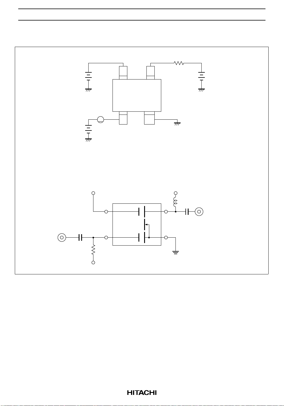
Test Circuit for Operating Items (I , |yfs|, Ciss, Coss, Crss, NF, PG)
V
G2 V
Gate 2
Drain
A
I
D
D(op)
Gate 1
Source
R
G
G1
Application Circuit
V = 6 to 0.3 V
AGC
BBFET
V = 9 V
DS
RFC
Output
Input
R
G
V = 9 V
GG
3
BB102M
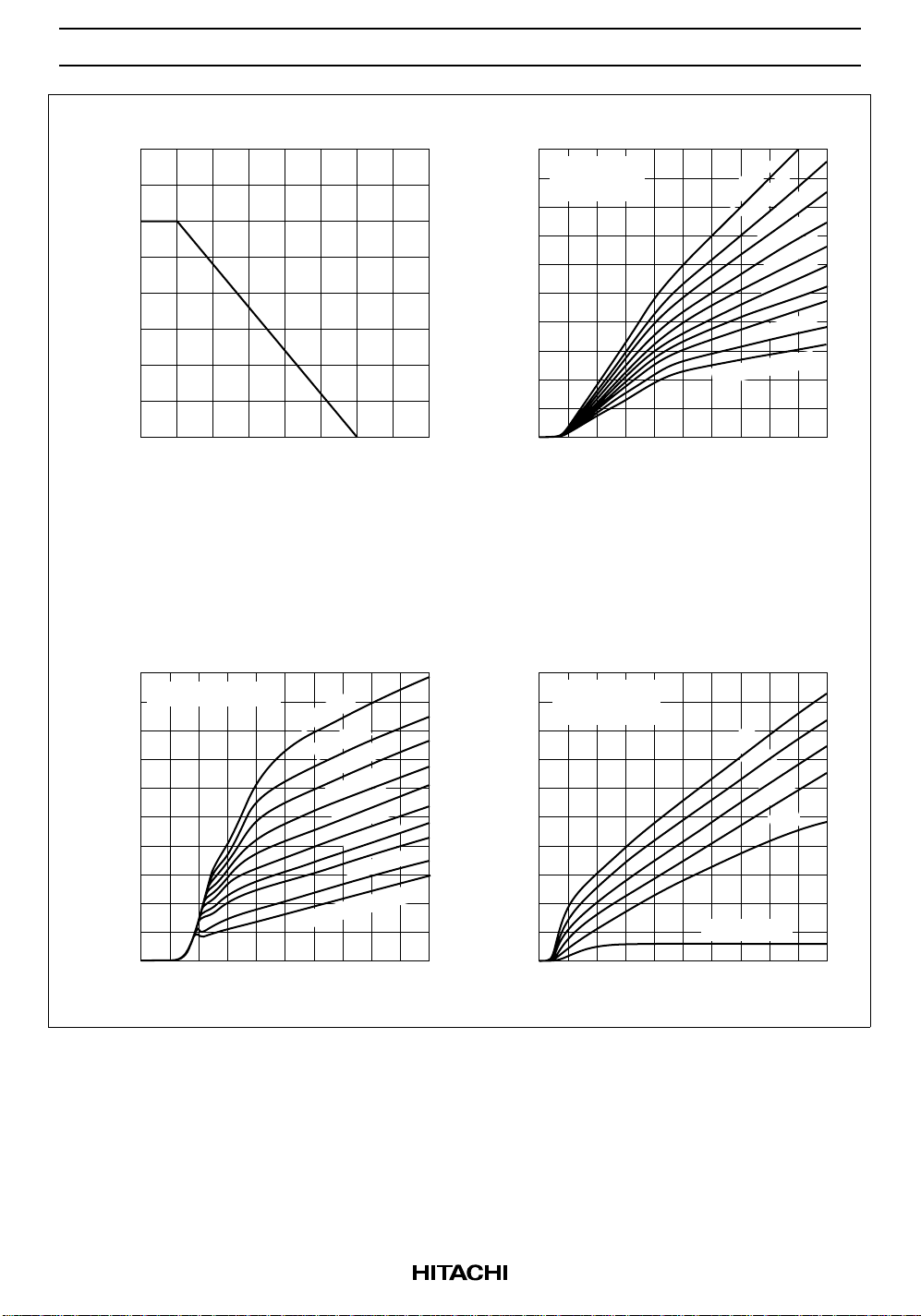
200
150
100
50
Maximum Channel Power
Dissipation Curve
25
Typical Output Characteristics
V = 6 V
G2S
V = V
G1 DS
20
D
15
10
Drain Current I (mA)
5
Ω
Ω
270 k
330 k
390 k
470 k
560 k
680 k
820 k
1 MΩ
1.5 MΩ
R = 2.2 M
G
Ω
Ω
Ω
Ω
Ω
Ω
Channel Power Dissipation Pch (mW)
0
50 100 150 200
Ambient Temperature Ta (°C)
Drain Current vs.
Gate2 to Source Voltage
25
V = V = 9 V
20
D
15
10
DS
G1
270 k
330 k
390 k
Ω
Ω
470 k
560 k
680 k
820 k
1 MΩ
Ω
Ω
Ω
1.5 MΩ
Drain Current I (mA)
5
G
R = 2.2 M
0
246810
Drain to Source Voltage V (V)
DS
Drain Current vs. Gate1 Voltage
20
V = 9 V
DS
R = 470 k
G
16
D
12
Ω
Ω
Ω
6 V
5 V
4 V
3 V
2 V
8
Ω
Drain Current I (mA)
4
V = 1 V
G2S
0
1.2 2.4 3.8 4.8 6.0
Gate2 to Source Voltage V (V)
G2S
0
246810
Gate1 Voltage V (V)
G1
4
 Loading...