


 Loading...
FUJITSU SEMICONDUCTOR
HARDWARE MANUAL
MB87J2120 & MB87P2020 -A
Lavender & Jasmine
Colour LCD/CRT/TV Controller
Specification
Fujitsu Microelectronics Europe GmbH
European MCU Design Centre (EMDC)
Am Siebenstein 6-10
D-63303 Dreieich-Buchschlag
Germany
Version: 1.8
File: MB87P2020.fm

MB87J2120, MB87P2020-A Hardware Manual
Revision History
Version |
|
Date |
Remark |
|
|
|
|
0.8 |
05. |
Apr. 2001 |
First Release |
|
|
|
|
0.9 |
27. |
Apr. 2001 |
Preliminary Release |
|
|
|
|
1.0 |
29. |
Jun. 2001 |
Overview Section and Register List reviewed |
|
|
|
SDC, PP, AAF, DIPA and ULB descriptions reviewed |
|
|
|
|
1.1 |
20. |
Jul. 2001 |
Register List improved, Lavender pinning added, overall review |
|
|
|
|
1.2 |
02. |
Aug. 2001 |
APLL spec included (CU) |
|
|
|
Review: overview, functional descriptions, register/command lists |
|
|
|
Preliminary AC Spec for Jasmine |
|
|
|
|
1.3 |
05. |
Oct. 2001 |
AC Spec for both devices, Lavender added/Jasmine reviewed |
|
|
|
Two pinning lists - sorted by name/pin number |
|
|
|
ULB DMA limit description (DMA FIFO limits vs. IPA block size) |
|
|
|
SDC Register description reviewed |
|
|
|
|
1.4 |
11. |
Oct 2001 |
Clarified AC Spec output characteristics (20/50pF conditions) |
|
|
|
|
1.5 |
27. |
Mar 2002 |
Pinning and additional registers for MB87P2020-A added |
|
|
|
Design description for changes in MB87P2020-A added |
|
|
|
AC Spec updated for MB87P2020-A |
|
|
|
|
1.6 |
05. |
Apr 2002 |
AC Spec for MB87J2120 updated |
|
|
|
|
1.7 |
22. |
Jul 2002 |
Description changed to MB87P2020-A |
|
|
|
|
1.8 |
18. |
Sep 2003 |
Display restriction description for physical colors added (1bpp, |
|
|
|
4bpp, RGB111 colour formats only) |
|
|
|
|
File: /usr/home/msed/gdc_dram/doc/manual/MB87P2020.fm
Copyright © 2001 by Fujitsu Microelectronics Europe GmbH
European MCU Design Centre (EMDC)
Am Siebenstein 6-10
D-63303 Dreieich-Buchschlag
Germany
This document contains information considered proprietary by the publisher. No part of this document may be copied, or reproduced in any form or by any means, or transferred to any third party without the prior written consent of the publisher. The document is subject to change without prior notice.
Page 12

Table of Contents
Table of Contents
PART A - Lavender and Jasmine Overview
1 Overview . . . . . . . . . . . . . . . . . . . . . . . . . . . . . . . . . . . . . . . . . . . . . . . . . . . . . . . . 15
1.1 Application overview. . . . . . . . . . . . . . . . . . . . . . . . . . . . . . . . . . . . . . . . . . . . . . . . . . . . . . . . 15 1.2 Jasmine/Lavender Block Diagram. . . . . . . . . . . . . . . . . . . . . . . . . . . . . . . . . . . . . . . . . . . . . . 15
2 Features and Functions . . . . . . . . . . . . . . . . . . . . . . . . . . . . . . . . . . . . . . . . . . . . 19 3 Clock supply and generation. . . . . . . . . . . . . . . . . . . . . . . . . . . . . . . . . . . . . . . . 21 4 Register and Command Overview . . . . . . . . . . . . . . . . . . . . . . . . . . . . . . . . . . . 23
4.1 Register Overview . . . . . . . . . . . . . . . . . . . . . . . . . . . . . . . . . . . . . . . . . . . . . . . . . . . . . . . . . . 23
4.2 Command Overview . . . . . . . . . . . . . . . . . . . . . . . . . . . . . . . . . . . . . . . . . . . . . . . . . . . . . . . . 23
PART B - Functional Descriptions
B-1 Clock Unit (CU) . . . . . . . . . . . . . . . . . . . . . . . . . . . . . . . . . . . . . . . . . 27
1 Functional Description . . . . . . . . . . . . . . . . . . . . . . . . . . . . . . . . . . . . . . . . . . . . |
29 |
1.1 Overview . . . . . . . . . . . . . . . . . . . . . . . . . . . . . . . . . . . . . . . . . . . . . . . . . . . . . . . . . . . . . . . . . 29
1.2 Reset Generation . . . . . . . . . . . . . . . . . . . . . . . . . . . . . . . . . . . . . . . . . . . . . . . . . . . . . . . . . . . 30
1.3 Register Set . . . . . . . . . . . . . . . . . . . . . . . . . . . . . . . . . . . . . . . . . . . . . . . . . . . . . . . . . . . . . . . 30
2 APLL Specification . . . . . . . . . . . . . . . . . . . . . . . . . . . . . . . . . . . . . . . . . . . . . . . |
33 |
2.1 Definitions . . . . . . . . . . . . . . . . . . . . . . . . . . . . . . . . . . . . . . . . . . . . . . . . . . . . . . . . . . . . . . . . 34
2.1.1 Phase Skew . . . . . . . . . . . . . . . . . . . . . . . . . . . . . . . . . . . . . . . . . . . . . . . . . . . . . . . . . . . . 34
2.1.2 Duty. . . . . . . . . . . . . . . . . . . . . . . . . . . . . . . . . . . . . . . . . . . . . . . . . . . . . . . . . . . . . . . . . . 34
2.1.3 Lock Up Time . . . . . . . . . . . . . . . . . . . . . . . . . . . . . . . . . . . . . . . . . . . . . . . . . . . . . . . . . . 34
2.1.4 Jitter. . . . . . . . . . . . . . . . . . . . . . . . . . . . . . . . . . . . . . . . . . . . . . . . . . . . . . . . . . . . . . . . . . 34
2.1.5 Variation in Output Cycle . . . . . . . . . . . . . . . . . . . . . . . . . . . . . . . . . . . . . . . . . . . . . . . . . 34
2.1.6 Maximum Power Consumption . . . . . . . . . . . . . . . . . . . . . . . . . . . . . . . . . . . . . . . . . . . . 35
2.2 Usage Instructions . . . . . . . . . . . . . . . . . . . . . . . . . . . . . . . . . . . . . . . . . . . . . . . . . . . . . . . . . . 35
3 Clock Setup and Configuration . . . . . . . . . . . . . . . . . . . . . . . . . . . . . . . . . . . . . |
36 |
3.1 Configurable Circuitry . . . . . . . . . . . . . . . . . . . . . . . . . . . . . . . . . . . . . . . . . . . . . . . . . . . . . . . 36 3.2 Clock Unit Programming Sequence . . . . . . . . . . . . . . . . . . . . . . . . . . . . . . . . . . . . . . . . . . . . 37 3.3 Application Notes . . . . . . . . . . . . . . . . . . . . . . . . . . . . . . . . . . . . . . . . . . . . . . . . . . . . . . . . . . 38
B-2 User Logic Bus Controller (ULB) . . . . . . . . . . . . . . . . . . . . . . . . . . 39
Table of Contents |
Page 1 |

MB87J2120, MB87P2020-A Hardware Manual
1 Functional description. . . . . . . . . . . . . . . . . . . . . . . . . . . . . . . . . . . . . . . . . . . . . .41
1.1 ULB functions . . . . . . . . . . . . . . . . . . . . . . . . . . . . . . . . . . . . . . . . . . . . . . . . . . . . . . . . . . . . . . 41 1.2 ULB overview . . . . . . . . . . . . . . . . . . . . . . . . . . . . . . . . . . . . . . . . . . . . . . . . . . . . . . . . . . . . . . 42 1.3 Signal synchronisation between MCU and display controller . . . . . . . . . . . . . . . . . . . . . . . . . 44 1.3.1 Write synchronization for Lavender and Jasmine . . . . . . . . . . . . . . . . . . . . . . . . . . . . . . 44 1.3.2 Read synchronization . . . . . . . . . . . . . . . . . . . . . . . . . . . . . . . . . . . . . . . . . . . . . . . . . . . . 45 1.3.3 DMA and interrupt signal synchronization . . . . . . . . . . . . . . . . . . . . . . . . . . . . . . . . . . . 45 1.3.4 Output signal configuration . . . . . . . . . . . . . . . . . . . . . . . . . . . . . . . . . . . . . . . . . . . . . . . 46 1.4 Address decoding . . . . . . . . . . . . . . . . . . . . . . . . . . . . . . . . . . . . . . . . . . . . . . . . . . . . . . . . . . . 46 1.4.1 Overview . . . . . . . . . . . . . . . . . . . . . . . . . . . . . . . . . . . . . . . . . . . . . . . . . . . . . . . . . . . . . 46 1.4.2 Register space . . . . . . . . . . . . . . . . . . . . . . . . . . . . . . . . . . . . . . . . . . . . . . . . . . . . . . . . . . 47 1.4.3 SDRAM space . . . . . . . . . . . . . . . . . . . . . . . . . . . . . . . . . . . . . . . . . . . . . . . . . . . . . . . . . 49 1.4.4 Display controller bus access types (word, halfword, byte). . . . . . . . . . . . . . . . . . . . . . . 51 1.4.5 Display controller data modes (32/16 Bit interface) . . . . . . . . . . . . . . . . . . . . . . . . . . . . 52 1.5 Command decoding and execution . . . . . . . . . . . . . . . . . . . . . . . . . . . . . . . . . . . . . . . . . . . . . . 53 1.5.1 Command and data interface to MCU . . . . . . . . . . . . . . . . . . . . . . . . . . . . . . . . . . . . . . . 53 1.5.2 Command execution and programming . . . . . . . . . . . . . . . . . . . . . . . . . . . . . . . . . . . . . . 55 1.5.3 Structure of command controller . . . . . . . . . . . . . . . . . . . . . . . . . . . . . . . . . . . . . . . . . . . 58 1.5.4 Display controller commands. . . . . . . . . . . . . . . . . . . . . . . . . . . . . . . . . . . . . . . . . . . . . . 59 1.5.5 Registers and flags regarding command execution . . . . . . . . . . . . . . . . . . . . . . . . . . . . . 60 1.6 Flag and interrupt handling . . . . . . . . . . . . . . . . . . . . . . . . . . . . . . . . . . . . . . . . . . . . . . . . . . . . 61 1.6.1 Flag and interrupt registers . . . . . . . . . . . . . . . . . . . . . . . . . . . . . . . . . . . . . . . . . . . . . . . . 61 1.6.2 Interrupt controller configuration . . . . . . . . . . . . . . . . . . . . . . . . . . . . . . . . . . . . . . . . . . . 61 1.6.3 Interrupt generation . . . . . . . . . . . . . . . . . . . . . . . . . . . . . . . . . . . . . . . . . . . . . . . . . . . . . 62 1.6.4 Interrupt configuration example . . . . . . . . . . . . . . . . . . . . . . . . . . . . . . . . . . . . . . . . . . . . 63 1.6.5 Display controller flags . . . . . . . . . . . . . . . . . . . . . . . . . . . . . . . . . . . . . . . . . . . . . . . . . . 64 1.7 DMA handling . . . . . . . . . . . . . . . . . . . . . . . . . . . . . . . . . . . . . . . . . . . . . . . . . . . . . . . . . . . . . 64 1.7.1 DMA interface . . . . . . . . . . . . . . . . . . . . . . . . . . . . . . . . . . . . . . . . . . . . . . . . . . . . . . . . . 64 1.7.2 DMA modes . . . . . . . . . . . . . . . . . . . . . . . . . . . . . . . . . . . . . . . . . . . . . . . . . . . . . . . . . . . 64 1.7.3 DMA settings . . . . . . . . . . . . . . . . . . . . . . . . . . . . . . . . . . . . . . . . . . . . . . . . . . . . . . . . . . 66 1.7.4 DMA programming examples . . . . . . . . . . . . . . . . . . . . . . . . . . . . . . . . . . . . . . . . . . . . . 68
2 ULB register set . . . . . . . . . . . . . . . . . . . . . . . . . . . . . . . . . . . . . . . . . . . . . . . . . . .71
2.1 Description . . . . . . . . . . . . . . . . . . . . . . . . . . . . . . . . . . . . . . . . . . . . . . . . . . . . . . . . . . . . . . . . 71 2.2 ULB initialization . . . . . . . . . . . . . . . . . . . . . . . . . . . . . . . . . . . . . . . . . . . . . . . . . . . . . . . . . . . 74
B-3 SDRAM Controller (SDC) . . . . . . . . . . . . . . . . . . . . . . . . . . . . . . . . 75
1 Function Description . . . . . . . . . . . . . . . . . . . . . . . . . . . . . . . . . . . . . . . . . . . . . . .77
1.1 Overview . . . . . . . . . . . . . . . . . . . . . . . . . . . . . . . . . . . . . . . . . . . . . . . . . . . . . . . . . . . . . . . . . . 77
Page 2

Table of Contents
1.2 Arbitration . . . . . . . . . . . . . . . . . . . . . . . . . . . . . . . . . . . . . . . . . . . . . . . . . . . . . . . . . . . . . . . . 78 1.3 SDRAM Timing . . . . . . . . . . . . . . . . . . . . . . . . . . . . . . . . . . . . . . . . . . . . . . . . . . . . . . . . . . . 78 1.4 Sequencer for Refresh and Power Down . . . . . . . . . . . . . . . . . . . . . . . . . . . . . . . . . . . . . . . . . 79 1.5 Address Mapping . . . . . . . . . . . . . . . . . . . . . . . . . . . . . . . . . . . . . . . . . . . . . . . . . . . . . . . . . . . 81 1.5.1 Elucidations regarding Address Mapping . . . . . . . . . . . . . . . . . . . . . . . . . . . . . . . . . . . . . 83
2 SDRAM Ports . . . . . . . . . . . . . . . . . . . . . . . . . . . . . . . . . . . . . . . . . . . . . . . . . . . . 92
2.1 External SDRAM I-/O-Pads with configurable sampling Time (Lavender) . . . . . . . . . . . . . . 92 2.2 Integrated SDRAM Implementation (Jasmine) . . . . . . . . . . . . . . . . . . . . . . . . . . . . . . . . . . . . 93
3 Configuration . . . . . . . . . . . . . . . . . . . . . . . . . . . . . . . . . . . . . . . . . . . . . . . . . . . . 94
3.1 Register Summary . . . . . . . . . . . . . . . . . . . . . . . . . . . . . . . . . . . . . . . . . . . . . . . . . . . . . . . . . . 94 3.2 Core clock dependent Timing Configuration . . . . . . . . . . . . . . . . . . . . . . . . . . . . . . . . . . . . . 95 3.2.1 General Setup . . . . . . . . . . . . . . . . . . . . . . . . . . . . . . . . . . . . . . . . . . . . . . . . . . . . . . . . . . 95 3.2.2 Refresh Configuration for integrated DRAM (Jasmine). . . . . . . . . . . . . . . . . . . . . . . . . . 95
B-4 Pixel Processor (PP). . . . . . . . . . . . . . . . . . . . . . . . . . . . . . . . . . . . . . 97
1 Functional Description . . . . . . . . . . . . . . . . . . . . . . . . . . . . . . . . . . . . . . . . . . . . |
99 |
1.1 Overview . . . . . . . . . . . . . . . . . . . . . . . . . . . . . . . . . . . . . . . . . . . . . . . . . . . . . . . . . . . . . . . . . 99 1.1.1 PP Structure. . . . . . . . . . . . . . . . . . . . . . . . . . . . . . . . . . . . . . . . . . . . . . . . . . . . . . . . . . . . 99 1.1.2 Function of submodules . . . . . . . . . . . . . . . . . . . . . . . . . . . . . . . . . . . . . . . . . . . . . . . . . 100 1.2 Configuration Registers . . . . . . . . . . . . . . . . . . . . . . . . . . . . . . . . . . . . . . . . . . . . . . . . . . . . . 101 1.3 Special Command Options . . . . . . . . . . . . . . . . . . . . . . . . . . . . . . . . . . . . . . . . . . . . . . . . . . 103 1.3.1 Bitmap Mirror . . . . . . . . . . . . . . . . . . . . . . . . . . . . . . . . . . . . . . . . . . . . . . . . . . . . . . . . . 103 1.3.2 Bitmap Direction . . . . . . . . . . . . . . . . . . . . . . . . . . . . . . . . . . . . . . . . . . . . . . . . . . . . . . . 103
2 Format Definitions . . . . . . . . . . . . . . . . . . . . . . . . . . . . . . . . . . . . . . . . . . . . . . . 104
2.1 Legend of symbols. . . . . . . . . . . . . . . . . . . . . . . . . . . . . . . . . . . . . . . . . . . . . . . . . . . . . . . . . 104 2.2 Data Formats at ULB Interface . . . . . . . . . . . . . . . . . . . . . . . . . . . . . . . . . . . . . . . . . . . . . . . 105 2.3 Data Formats for Video RAM / SDC Interface . . . . . . . . . . . . . . . . . . . . . . . . . . . . . . . . . . . 106
B-5 Antialiasing Filter (AAF) . . . . . . . . . . . . . . . . . . . . . . . . . . . . . . . . 109
1 Functional Description . . . . . . . . . . . . . . . . . . . . . . . . . . . . . . . . . . . . . . . . . . . |
111 |
1.1 AAF Overview. . . . . . . . . . . . . . . . . . . . . . . . . . . . . . . . . . . . . . . . . . . . . . . . . . . . . . . . . . . . 111
1.1.1 Top Level Structure. . . . . . . . . . . . . . . . . . . . . . . . . . . . . . . . . . . . . . . . . . . . . . . . . . . . . 111
1.1.2 AAU Function . . . . . . . . . . . . . . . . . . . . . . . . . . . . . . . . . . . . . . . . . . . . . . . . . . . . . . . . . 112
1.2 Configuration Registers . . . . . . . . . . . . . . . . . . . . . . . . . . . . . . . . . . . . . . . . . . . . . . . . . . . . . 113
1.3 Application Notes . . . . . . . . . . . . . . . . . . . . . . . . . . . . . . . . . . . . . . . . . . . . . . . . . . . . . . . . . 114
1.3.1 Restrictions due to Usage of AAF . . . . . . . . . . . . . . . . . . . . . . . . . . . . . . . . . . . . . . . . . 114
Table of Contents |
Page 3 |

MB87J2120, MB87P2020-A Hardware Manual
1.3.2 Supported Colour Formats . . . . . . . . . . . . . . . . . . . . . . . . . . . . . . . . . . . . . . . . . . . . . . . 115
1.3.3 Related SDC Configuration . . . . . . . . . . . . . . . . . . . . . . . . . . . . . . . . . . . . . . . . . . . . . . 115
B-6 Direct and Indirect Physical Memory Access Unit (DIPA) . . . . . 117
1 Overview. . . . . . . . . . . . . . . . . . . . . . . . . . . . . . . . . . . . . . . . . . . . . . . . . . . . . . . .119
2 Configuration Registers . . . . . . . . . . . . . . . . . . . . . . . . . . . . . . . . . . . . . . . . . . .121
2.1 Register List . . . . . . . . . . . . . . . . . . . . . . . . . . . . . . . . . . . . . . . . . . . . . . . . . . . . . . . . . . . . . . 121
2.2 Recommended Settings . . . . . . . . . . . . . . . . . . . . . . . . . . . . . . . . . . . . . . . . . . . . . . . . . . . . . . 121
2.3 Related Settings and Informations . . . . . . . . . . . . . . . . . . . . . . . . . . . . . . . . . . . . . . . . . . . . . 122
B-7 Video Interface Controller (VIC) . . . . . . . . . . . . . . . . . . . . . . . . . . 123
1 Introduction . . . . . . . . . . . . . . . . . . . . . . . . . . . . . . . . . . . . . . . . . . . . . . . . . . . . .125
1.1 Video Interface Controller functions and features . . . . . . . . . . . . . . . . . . . . . . . . . . . . . . . . . 125 1.2 Video data handling . . . . . . . . . . . . . . . . . . . . . . . . . . . . . . . . . . . . . . . . . . . . . . . . . . . . . . . . 125
2 VIC Description . . . . . . . . . . . . . . . . . . . . . . . . . . . . . . . . . . . . . . . . . . . . . . . . . .127
2.1 Data Input Formats . . . . . . . . . . . . . . . . . . . . . . . . . . . . . . . . . . . . . . . . . . . . . . . . . . . . . . . . . 127 2.2 Data format in Video RAM (SDRAM). . . . . . . . . . . . . . . . . . . . . . . . . . . . . . . . . . . . . . . . . . 129 2.3 Data Input Timing . . . . . . . . . . . . . . . . . . . . . . . . . . . . . . . . . . . . . . . . . . . . . . . . . . . . . . . . . . 130 2.3.1 Videoscaler-Mode . . . . . . . . . . . . . . . . . . . . . . . . . . . . . . . . . . . . . . . . . . . . . . . . . . . . . 130 2.3.2 CCIR-Mode . . . . . . . . . . . . . . . . . . . . . . . . . . . . . . . . . . . . . . . . . . . . . . . . . . . . . . . . . . 131 2.3.3 External-Timing-mode . . . . . . . . . . . . . . . . . . . . . . . . . . . . . . . . . . . . . . . . . . . . . . . . . . 132
3 VIC settings . . . . . . . . . . . . . . . . . . . . . . . . . . . . . . . . . . . . . . . . . . . . . . . . . . . . .135
3.1 Register list . . . . . . . . . . . . . . . . . . . . . . . . . . . . . . . . . . . . . . . . . . . . . . . . . . . . . . . . . . . . . . . 135 3.2 Register Description . . . . . . . . . . . . . . . . . . . . . . . . . . . . . . . . . . . . . . . . . . . . . . . . . . . . . . . . 139
B-8 Graphic Processing Unit (GPU) . . . . . . . . . . . . . . . . . . . . . . . . . . . 149
1 Functional Description . . . . . . . . . . . . . . . . . . . . . . . . . . . . . . . . . . . . . . . . . . . .151
1.1 GPU Features . . . . . . . . . . . . . . . . . . . . . . . . . . . . . . . . . . . . . . . . . . . . . . . . . . . . . . . . . . . . . 151
1.2 GPU Overview . . . . . . . . . . . . . . . . . . . . . . . . . . . . . . . . . . . . . . . . . . . . . . . . . . . . . . . . . . . . 152
1.2.1 Top Level Structure . . . . . . . . . . . . . . . . . . . . . . . . . . . . . . . . . . . . . . . . . . . . . . . . . . . . 152
1.2.2 DFU Function . . . . . . . . . . . . . . . . . . . . . . . . . . . . . . . . . . . . . . . . . . . . . . . . . . . . . . . . . 152
1.2.3 CCU Function. . . . . . . . . . . . . . . . . . . . . . . . . . . . . . . . . . . . . . . . . . . . . . . . . . . . . . . . . 153
1.2.4 LSA Function . . . . . . . . . . . . . . . . . . . . . . . . . . . . . . . . . . . . . . . . . . . . . . . . . . . . . . . . . 154
1.2.5 BSF Function . . . . . . . . . . . . . . . . . . . . . . . . . . . . . . . . . . . . . . . . . . . . . . . . . . . . . . . . . 154
2 Color Space Concept . . . . . . . . . . . . . . . . . . . . . . . . . . . . . . . . . . . . . . . . . . . . . .156
Page 4

Table of Contents
2.1 Background . . . . . . . . . . . . . . . . . . . . . . . . . . . . . . . . . . . . . . . . . . . . . . . . . . . . . . . . . . . . . . 156 2.2 Data Flow for Color Space Conversion within GPU. . . . . . . . . . . . . . . . . . . . . . . . . . . . . . . 156 2.3 Mapping from Logical to Intermediate Color Space . . . . . . . . . . . . . . . . . . . . . . . . . . . . . . . 157 2.4 Mapping from Intermediate to Physical Color Space . . . . . . . . . . . . . . . . . . . . . . . . . . . . . . 157
3 GPU Control Information . . . . . . . . . . . . . . . . . . . . . . . . . . . . . . . . . . . . . . . . . 162
3.1 Layer Description Record . . . . . . . . . . . . . . . . . . . . . . . . . . . . . . . . . . . . . . . . . . . . . . . . . . . 162 3.2 Merging Description Record . . . . . . . . . . . . . . . . . . . . . . . . . . . . . . . . . . . . . . . . . . . . . . . . . 164 3.3 Display Interface Record . . . . . . . . . . . . . . . . . . . . . . . . . . . . . . . . . . . . . . . . . . . . . . . . . . . . 165 3.4 Supported Physical Color Space / Bit Stream Format Combinations . . . . . . . . . . . . . . . . . . 167 3.5 Twin Display Mode . . . . . . . . . . . . . . . . . . . . . . . . . . . . . . . . . . . . . . . . . . . . . . . . . . . . . . . . 167 3.6 Scan Modes . . . . . . . . . . . . . . . . . . . . . . . . . . . . . . . . . . . . . . . . . . . . . . . . . . . . . . . . . . . . . . 168 3.7 YUV to RGB conversion . . . . . . . . . . . . . . . . . . . . . . . . . . . . . . . . . . . . . . . . . . . . . . . . . . . . 171
3.7.1 YUV422 Demultiplexing and Chrominance Interpolation . . . . . . . . . . . . . . . . . . . . . . . 171 3.7.2 Matrix Multiplication . . . . . . . . . . . . . . . . . . . . . . . . . . . . . . . . . . . . . . . . . . . . . . . . . . . 172 3.7.3 Inverse Gamma Correction . . . . . . . . . . . . . . . . . . . . . . . . . . . . . . . . . . . . . . . . . . . . . . . 172 3.8 Duty Ratio Modulation . . . . . . . . . . . . . . . . . . . . . . . . . . . . . . . . . . . . . . . . . . . . . . . . . . . . . 173 3.8.1 Working Principle . . . . . . . . . . . . . . . . . . . . . . . . . . . . . . . . . . . . . . . . . . . . . . . . . . . . . . 173 3.8.2 Usage. . . . . . . . . . . . . . . . . . . . . . . . . . . . . . . . . . . . . . . . . . . . . . . . . . . . . . . . . . . . . . . . 174 3.9 Master Timing Information . . . . . . . . . . . . . . . . . . . . . . . . . . . . . . . . . . . . . . . . . . . . . . . . . . 175 3.10 Generation of Sync Signals . . . . . . . . . . . . . . . . . . . . . . . . . . . . . . . . . . . . . . . . . . . . . . . . . 176 3.10.1 Overview . . . . . . . . . . . . . . . . . . . . . . . . . . . . . . . . . . . . . . . . . . . . . . . . . . . . . . . . . . . . 176 3.10.2 Position Matching . . . . . . . . . . . . . . . . . . . . . . . . . . . . . . . . . . . . . . . . . . . . . . . . . . . . . 176 3.10.3 Sequence Matching . . . . . . . . . . . . . . . . . . . . . . . . . . . . . . . . . . . . . . . . . . . . . . . . . . . . 177 3.10.4 Combining First-Stage Sync Signals . . . . . . . . . . . . . . . . . . . . . . . . . . . . . . . . . . . . . . 178 3.10.5 Sync Signal Delay Adjustment . . . . . . . . . . . . . . . . . . . . . . . . . . . . . . . . . . . . . . . . . . . 180 3.11 Pixel Clock Gating. . . . . . . . . . . . . . . . . . . . . . . . . . . . . . . . . . . . . . . . . . . . . . . . . . . . . . . . 180 3.12 Numerical Mnemonic Definitions . . . . . . . . . . . . . . . . . . . . . . . . . . . . . . . . . . . . . . . . . . . . 181 3.12.1 Color Space Code . . . . . . . . . . . . . . . . . . . . . . . . . . . . . . . . . . . . . . . . . . . . . . . . . . . . . 181 3.12.2 Bit Stream Format Code . . . . . . . . . . . . . . . . . . . . . . . . . . . . . . . . . . . . . . . . . . . . . . . . 182 3.12.3 Scan Mode Code . . . . . . . . . . . . . . . . . . . . . . . . . . . . . . . . . . . . . . . . . . . . . . . . . . . . . . 182 3.13 Bit to Color Channel Assignment . . . . . . . . . . . . . . . . . . . . . . . . . . . . . . . . . . . . . . . . . . . . 183 3.14 GPU Signal to GDC Pin Assignment . . . . . . . . . . . . . . . . . . . . . . . . . . . . . . . . . . . . . . . . . 184 3.14.1 Multi-Purpose Digital Signals. . . . . . . . . . . . . . . . . . . . . . . . . . . . . . . . . . . . . . . . . . . . 184 3.14.2 Analog Pixel Data . . . . . . . . . . . . . . . . . . . . . . . . . . . . . . . . . . . . . . . . . . . . . . . . . . . . . 184 3.14.3 Dedicated Sync Signals. . . . . . . . . . . . . . . . . . . . . . . . . . . . . . . . . . . . . . . . . . . . . . . . . 184 3.14.4 Sync Mixer connections . . . . . . . . . . . . . . . . . . . . . . . . . . . . . . . . . . . . . . . . . . . . . . . . 185 3.14.5 Color Key Output . . . . . . . . . . . . . . . . . . . . . . . . . . . . . . . . . . . . . . . . . . . . . . . . . . . . . 185
4 GPU Register Set . . . . . . . . . . . . . . . . . . . . . . . . . . . . . . . . . . . . . . . . . . . . . . . . 187
Table of Contents |
Page 5 |

MB87J2120, MB87P2020-A Hardware Manual
4.1 Description . . . . . . . . . . . . . . . . . . . . . . . . . . . . . . . . . . . . . . . . . . . . . . . . . . . . . . . . . . . . . . . 187
4.2 Determination of Register Contents . . . . . . . . . . . . . . . . . . . . . . . . . . . . . . . . . . . . . . . . . . . . 194
4.2.1 Values Derived from Display Specs. . . . . . . . . . . . . . . . . . . . . . . . . . . . . . . . . . . . . . . . 194
4.2.2 Values Determined by Application . . . . . . . . . . . . . . . . . . . . . . . . . . . . . . . . . . . . . . . . 196
4.2.3 User preferences . . . . . . . . . . . . . . . . . . . . . . . . . . . . . . . . . . . . . . . . . . . . . . . . . . . . . . . 197
4.3 GPU Initialization Sequence . . . . . . . . . . . . . . . . . . . . . . . . . . . . . . . . . . . . . . . . . . . . . . . . . . 197
5 Bandwidth Considerations . . . . . . . . . . . . . . . . . . . . . . . . . . . . . . . . . . . . . . . . .198
5.1 Processing Bandwidth . . . . . . . . . . . . . . . . . . . . . . . . . . . . . . . . . . . . . . . . . . . . . . . . . . . . . . . 198
5.1.1 Average Bandwidth . . . . . . . . . . . . . . . . . . . . . . . . . . . . . . . . . . . . . . . . . . . . . . . . . . . . 198
5.1.2 Peak Bandwidth . . . . . . . . . . . . . . . . . . . . . . . . . . . . . . . . . . . . . . . . . . . . . . . . . . . . . . . 198
5.2 Memory Bandwidth . . . . . . . . . . . . . . . . . . . . . . . . . . . . . . . . . . . . . . . . . . . . . . . . . . . . . . . . 200
5.2.1 Average Bandwidth . . . . . . . . . . . . . . . . . . . . . . . . . . . . . . . . . . . . . . . . . . . . . . . . . . . . 201
5.2.2 Peak Bandwidth . . . . . . . . . . . . . . . . . . . . . . . . . . . . . . . . . . . . . . . . . . . . . . . . . . . . . . . 201
5.3 Recommendations . . . . . . . . . . . . . . . . . . . . . . . . . . . . . . . . . . . . . . . . . . . . . . . . . . . . . . . . . . 202
6 Functional Peculiarities. . . . . . . . . . . . . . . . . . . . . . . . . . . . . . . . . . . . . . . . . . . .204
6.1 Configuration Constraints . . . . . . . . . . . . . . . . . . . . . . . . . . . . . . . . . . . . . . . . . . . . . . . . . . . . 204
6.2 Bandwidth . . . . . . . . . . . . . . . . . . . . . . . . . . . . . . . . . . . . . . . . . . . . . . . . . . . . . . . . . . . . . . . . 204
6.3 Image Processing . . . . . . . . . . . . . . . . . . . . . . . . . . . . . . . . . . . . . . . . . . . . . . . . . . . . . . . . . . 205
6.4 Data Output . . . . . . . . . . . . . . . . . . . . . . . . . . . . . . . . . . . . . . . . . . . . . . . . . . . . . . . . . . . . . . . 206
6.5 Diagnostics . . . . . . . . . . . . . . . . . . . . . . . . . . . . . . . . . . . . . . . . . . . . . . . . . . . . . . . . . . . . . . . 206
7 Supported Displays . . . . . . . . . . . . . . . . . . . . . . . . . . . . . . . . . . . . . . . . . . . . . . .207
7.1 Passive Matrix LCD . . . . . . . . . . . . . . . . . . . . . . . . . . . . . . . . . . . . . . . . . . . . . . . . . . . . . . . . 208 7.2 Active Matrix (TFT) Displays . . . . . . . . . . . . . . . . . . . . . . . . . . . . . . . . . . . . . . . . . . . . . . . . 209 7.3 Electroluminescent Displays . . . . . . . . . . . . . . . . . . . . . . . . . . . . . . . . . . . . . . . . . . . . . . . . . . 210 7.4 Field Emission Displays . . . . . . . . . . . . . . . . . . . . . . . . . . . . . . . . . . . . . . . . . . . . . . . . . . . . . 212 7.5 Limitations for support . . . . . . . . . . . . . . . . . . . . . . . . . . . . . . . . . . . . . . . . . . . . . . . . . . . . . . 213
7.5.1 No Support due to VCOM Inversion . . . . . . . . . . . . . . . . . . . . . . . . . . . . . . . . . . . . . . . 213 7.5.2 Problems due to 5V CMOS Interfaces . . . . . . . . . . . . . . . . . . . . . . . . . . . . . . . . . . . . . . 213
B-9 Cold Cathode Fluorescence Light Driver (CCFL) . . . . . . . . . . . . 215
1 Introduction . . . . . . . . . . . . . . . . . . . . . . . . . . . . . . . . . . . . . . . . . . . . . . . . . . . . .217
2 Signal Waveform . . . . . . . . . . . . . . . . . . . . . . . . . . . . . . . . . . . . . . . . . . . . . . . . .219
2.1 General Description . . . . . . . . . . . . . . . . . . . . . . . . . . . . . . . . . . . . . . . . . . . . . . . . . . . . . . . . 219 2.2 Duration of the Phases . . . . . . . . . . . . . . . . . . . . . . . . . . . . . . . . . . . . . . . . . . . . . . . . . . . . . . 219 2.3 Pulse shape of FET1 and FET2. . . . . . . . . . . . . . . . . . . . . . . . . . . . . . . . . . . . . . . . . . . . . . . . 220
3 Register Description . . . . . . . . . . . . . . . . . . . . . . . . . . . . . . . . . . . . . . . . . . . . . .221
Page 6

Table of Contents
3.1 Overview . . . . . . . . . . . . . . . . . . . . . . . . . . . . . . . . . . . . . . . . . . . . . . . . . . . . . . . . . . . . . . . . 221
3.2 Control Bits . . . . . . . . . . . . . . . . . . . . . . . . . . . . . . . . . . . . . . . . . . . . . . . . . . . . . . . . . . . . . . 221
4 Application Notes . . . . . . . . . . . . . . . . . . . . . . . . . . . . . . . . . . . . . . . . . . . . . . . . 223
4.1 CCFL Setup Example . . . . . . . . . . . . . . . . . . . . . . . . . . . . . . . . . . . . . . . . . . . . . . . . . . . . . . 223
4.2 CCFL Protection . . . . . . . . . . . . . . . . . . . . . . . . . . . . . . . . . . . . . . . . . . . . . . . . . . . . . . . . . . 223
PART C - Pinning and Electrical Specification
1 Pinning and Buffer Types . . . . . . . . . . . . . . . . . . . . . . . . . . . . . . . . . . . . . . . . . 227
1.1 Pinning for MB87P2020-A . . . . . . . . . . . . . . . . . . . . . . . . . . . . . . . . . . . . . . . . . . . . . . . . . . 227 1.1.1 Pinning . . . . . . . . . . . . . . . . . . . . . . . . . . . . . . . . . . . . . . . . . . . . . . . . . . . . . . . . . . . . . . 227 1.1.2 Buffer types . . . . . . . . . . . . . . . . . . . . . . . . . . . . . . . . . . . . . . . . . . . . . . . . . . . . . . . . . . . 240 1.2 Pinning for MB87P2020 . . . . . . . . . . . . . . . . . . . . . . . . . . . . . . . . . . . . . . . . . . . . . . . . . . . . 240 1.2.1 Pinning . . . . . . . . . . . . . . . . . . . . . . . . . . . . . . . . . . . . . . . . . . . . . . . . . . . . . . . . . . . . . . 240 1.2.2 Buffer types . . . . . . . . . . . . . . . . . . . . . . . . . . . . . . . . . . . . . . . . . . . . . . . . . . . . . . . . . . . 253 1.3 Pinning for MB87J2120. . . . . . . . . . . . . . . . . . . . . . . . . . . . . . . . . . . . . . . . . . . . . . . . . . . . . 254 1.3.1 Pinning . . . . . . . . . . . . . . . . . . . . . . . . . . . . . . . . . . . . . . . . . . . . . . . . . . . . . . . . . . . . . . 254 1.3.2 Buffer Types . . . . . . . . . . . . . . . . . . . . . . . . . . . . . . . . . . . . . . . . . . . . . . . . . . . . . . . . . . 270
2 Electrical Specification . . . . . . . . . . . . . . . . . . . . . . . . . . . . . . . . . . . . . . . . . . . |
272 |
2.1 Maximum Ratings . . . . . . . . . . . . . . . . . . . . . . . . . . . . . . . . . . . . . . . . . . . . . . . . . . . . . . . . . 272 2.1.1 Power-on sequence . . . . . . . . . . . . . . . . . . . . . . . . . . . . . . . . . . . . . . . . . . . . . . . . . . . . . 272 2.1.2 External Signal Levels . . . . . . . . . . . . . . . . . . . . . . . . . . . . . . . . . . . . . . . . . . . . . . . . . . 273 2.1.3 APLL Power Supply Level . . . . . . . . . . . . . . . . . . . . . . . . . . . . . . . . . . . . . . . . . . . . . . . 273 2.1.4 DAC supply. . . . . . . . . . . . . . . . . . . . . . . . . . . . . . . . . . . . . . . . . . . . . . . . . . . . . . . . . . . 273 2.1.5 SDRAM Supply . . . . . . . . . . . . . . . . . . . . . . . . . . . . . . . . . . . . . . . . . . . . . . . . . . . . . . . 273
2.2 Recommended Operating Conditions . . . . . . . . . . . . . . . . . . . . . . . . . . . . . . . . . . . . . . . . . . 274 2.3 DC Characteristics . . . . . . . . . . . . . . . . . . . . . . . . . . . . . . . . . . . . . . . . . . . . . . . . . . . . . . . . . 274 2.4 Mounting / Soldering . . . . . . . . . . . . . . . . . . . . . . . . . . . . . . . . . . . . . . . . . . . . . . . . . . . . . . . 276 2.5 AC Characteristics . . . . . . . . . . . . . . . . . . . . . . . . . . . . . . . . . . . . . . . . . . . . . . . . . . . . . . . . . 277 2.5.1 Measurement Conditions . . . . . . . . . . . . . . . . . . . . . . . . . . . . . . . . . . . . . . . . . . . . . . . . 277 2.5.2 Definitions. . . . . . . . . . . . . . . . . . . . . . . . . . . . . . . . . . . . . . . . . . . . . . . . . . . . . . . . . . . . 277 2.5.3 Clock inputs . . . . . . . . . . . . . . . . . . . . . . . . . . . . . . . . . . . . . . . . . . . . . . . . . . . . . . . . . . 278 2.5.4 MCU User Logic Bus Interface . . . . . . . . . . . . . . . . . . . . . . . . . . . . . . . . . . . . . . . . . . . 280 2.5.5 Interrupt. . . . . . . . . . . . . . . . . . . . . . . . . . . . . . . . . . . . . . . . . . . . . . . . . . . . . . . . . . . . . . 282 2.5.6 DMA Control Ports . . . . . . . . . . . . . . . . . . . . . . . . . . . . . . . . . . . . . . . . . . . . . . . . . . . . . 283 2.5.7 Display Interface . . . . . . . . . . . . . . . . . . . . . . . . . . . . . . . . . . . . . . . . . . . . . . . . . . . . . . . 284 2.5.8 Video Input . . . . . . . . . . . . . . . . . . . . . . . . . . . . . . . . . . . . . . . . . . . . . . . . . . . . . . . . . . . 285 2.5.9 CCFL FET Driver . . . . . . . . . . . . . . . . . . . . . . . . . . . . . . . . . . . . . . . . . . . . . . . . . . . . . . 285
Table of Contents |
Page 7 |

MB87J2120, MB87P2020-A Hardware Manual
2.5.10 Serial Peripheral Bus . . . . . . . . . . . . . . . . . . . . . . . . . . . . . . . . . . . . . . . . . . . . . . . . . . 286
2.5.11 Special and Mode Pins . . . . . . . . . . . . . . . . . . . . . . . . . . . . . . . . . . . . . . . . . . . . . . . . . 286
2.5.12 SDRAM Ports (Lavender) . . . . . . . . . . . . . . . . . . . . . . . . . . . . . . . . . . . . . . . . . . . . . . 286
PART D - Appendix
D-1 Jasmine Command and Register Description. . . . . . . . . . . . . . . . 291
1 Register Description . . . . . . . . . . . . . . . . . . . . . . . . . . . . . . . . . . . . . . . . . . . . . .293
2 Flag Description. . . . . . . . . . . . . . . . . . . . . . . . . . . . . . . . . . . . . . . . . . . . . . . . . .321
3 Command Description . . . . . . . . . . . . . . . . . . . . . . . . . . . . . . . . . . . . . . . . . . . .325
3.1 Command List . . . . . . . . . . . . . . . . . . . . . . . . . . . . . . . . . . . . . . . . . . . . . . . . . . . . . . . . . . . . . 325
3.2 Command and I/O Control . . . . . . . . . . . . . . . . . . . . . . . . . . . . . . . . . . . . . . . . . . . . . . . . . . . 332
D-2 Hints and restrictions for Lavender and Jasmine . . . . . . . . . . . . 333
1 Special hints . . . . . . . . . . . . . . . . . . . . . . . . . . . . . . . . . . . . . . . . . . . . . . . . . . . . .335
1.1 IPA resistance against wrong settings. . . . . . . . . . . . . . . . . . . . . . . . . . . . . . . . . . . . . . . . . . . 335 1.2 ULB_DREQ pin timing to host MCU . . . . . . . . . . . . . . . . . . . . . . . . . . . . . . . . . . . . . . . . . . 335 1.3 CLKPDR master reset. . . . . . . . . . . . . . . . . . . . . . . . . . . . . . . . . . . . . . . . . . . . . . . . . . . . . . . 336 1.4 MAU (Memory Access Unit) commands . . . . . . . . . . . . . . . . . . . . . . . . . . . . . . . . . . . . . . . . 336 1.5 Pixel Processor (PP) double buffering . . . . . . . . . . . . . . . . . . . . . . . . . . . . . . . . . . . . . . . . . . 337 1.6 Robustness of ULB_RDY signal . . . . . . . . . . . . . . . . . . . . . . . . . . . . . . . . . . . . . . . . . . . . . . 338 1.7 Robustness of command pipeline against software errors . . . . . . . . . . . . . . . . . . . . . . . . . . . 339 1.8 DMA resistance against wrong settings . . . . . . . . . . . . . . . . . . . . . . . . . . . . . . . . . . . . . . . . . 339
2 Restrictions. . . . . . . . . . . . . . . . . . . . . . . . . . . . . . . . . . . . . . . . . . . . . . . . . . . . . .341
2.1 ESD characteristics for I/O buffers . . . . . . . . . . . . . . . . . . . . . . . . . . . . . . . . . . . . . . . . . . . . . 341 2.2 Command FSM . . . . . . . . . . . . . . . . . . . . . . . . . . . . . . . . . . . . . . . . . . . . . . . . . . . . . . . . . . . . 343 2.3 GPU mastertiming synchronization . . . . . . . . . . . . . . . . . . . . . . . . . . . . . . . . . . . . . . . . . . . . 343 2.4 Read limitation for 16 Bit data interface to MCU. . . . . . . . . . . . . . . . . . . . . . . . . . . . . . . . . . 344 2.5 SDC sequencer readback. . . . . . . . . . . . . . . . . . . . . . . . . . . . . . . . . . . . . . . . . . . . . . . . . . . . . 346 2.6 Direct SDRAM access with 16bit and 8bit data mode . . . . . . . . . . . . . . . . . . . . . . . . . . . . . . 346 2.7 Input FIFO read in 16bit mode . . . . . . . . . . . . . . . . . . . . . . . . . . . . . . . . . . . . . . . . . . . . . . . . 347 2.8 ULB_DSTP pin function. . . . . . . . . . . . . . . . . . . . . . . . . . . . . . . . . . . . . . . . . . . . . . . . . . . . . 347 2.9 Software Reset for command execution . . . . . . . . . . . . . . . . . . . . . . . . . . . . . . . . . . . . . . . . . 348 2.10 AAF settings double buffering . . . . . . . . . . . . . . . . . . . . . . . . . . . . . . . . . . . . . . . . . . . . . . . 349 2.11 Pixel Engine (PE) Commands . . . . . . . . . . . . . . . . . . . . . . . . . . . . . . . . . . . . . . . . . . . . . . . 350 2.12 Pixel read back commands (GetPixel, XChPixel) . . . . . . . . . . . . . . . . . . . . . . . . . . . . . . . . 351
Page 8
Table of Contents
2.13 Display Interface Re-configuration . . . . . . . . . . . . . . . . . . . . . . . . . . . . . . . . . . . . . . . . . . . 353 2.14 Display Limitation for physical color depths . . . . . . . . . . . . . . . . . . . . . . . . . . . . . . . . . . . 354
D-3 Abbreviations . . . . . . . . . . . . . . . . . . . . . . . . . . . . . . . . . . . . . . . . . . 355
Table of Contents |
Page 9 |

MB87J2120, MB87P2020-A Hardware Manual
Page 10

PART A - Lavender and Jasmine
Overview
Page 13

MB87J2120, MB87P2020-A Hardware Manual
Page 14

Graphic Controller Overview
1 Overview
1.1Application overview
The MB87J2120 "Lavender" and MB87P2020-A “Jasmine” are colour LCD/CRT graphic display control-
lers (GDCs)1 interfacing to MB91xxxx micro controller family and support a wide range of display devices. The architecture is designed to meet the low cost, low power requirements in embedded and especially in
automotive2 applications.
Lavender and Jasmine support almost all LCD panel types and CRTs or other progressive scanned3 monitors/displays which can be connected via the digital or analog RGB output. Products requiring video/camera input can take advantage of the supported digital video interface. The graphic instruction set is optimized for minimal traffic at the MCU interface because it’s the most important performance issue of co-processing graphic acceleration systems. Lavender uses external connected SDRAM, Jasmine is a compatible GDC version with integrated SDRAM (1MByte) and comes with additional features.
Lavender and Jasmine support a set of 2D drawing functions with built in Pixel Processor, a video scaler interface, units for physical and direct video memory access and a powerful video output stream formatter for the greatest variety of connectable displays.
Figure 1-1 displays an application block diagram in order to show the connection possibilities of Jasmine. For Lavender external SDRAM connection is required in addition.
1.2Jasmine/Lavender Block Diagram
Figure 1-2 shows all main components of Jasmine/Lavender graphic controllers. The User Logic Bus controller (ULB), Clock Unit (CU) and Serial Peripheral Bus (SPB) are connected to the User Logic Bus interface of 32 bit Fujitsu RISC microprocessors. 32 and 16 bit access modes are supported.
Table 1-1: GDC components
|
Shortcut |
|
Meaning |
Main Function |
|
|
|
|
|
CCFL |
Cold Cathode Fluorescence |
Cold cathode driver for display backlight |
||
|
|
Lamp |
|
|
|
|
|
|
|
CU |
Clock Unit |
Clock gearing and supply, Power save |
||
|
|
|
|
|
DAC |
Digital Analog Converter |
Digital to analog conversion for analog |
||
|
|
|
|
display |
|
|
|
|
|
DPA (part of DIPA) |
Direct Physical memory Access |
Memory mapped SDRAM access with |
||
|
|
|
|
address decoding |
|
|
|
|
|
GPU |
Graphics Processing Unit |
Frame buffer reader which converts to |
||
|
|
|
|
video data format required by display |
|
|
|
|
|
DFU (part of GPU) |
Data Fetch Unit |
Graphic/video data acquisition |
||
|
|
|
|
|
CCU (part of GPU) |
Colour Conversion Unit |
Colour format conversion to common |
||
|
|
|
|
intermediate overlay format |
|
|
|
|
|
|
|
|
|
|
1.The general term ’graphic display controller’ or its abbreviation ’GDC’ is used in this manual to identify both devices. Mainly this is used to emphasize its common features.
2.Both display controllers have an enhanced temperature range of -40 to 85 oC.
3.TV conform output (interlaced) is also possible with half the vertical resolution (line doubling).
Overview |
Page 15 |

MB87J2120, MB87P2020-A Hardware Manual
Host MCU
MB91xxxx
Digital Video
MB87P2020 or MB87J2120 (Jasmine or Lavender)
RGB Analog
Video Scaler
e.g. VPX3220A, SAA7111A
Figure 1-1: Application overview
Table 1-1: GDC components
|
Shortcut |
Meaning |
Main Function |
|
|
|
|
|
LSA (part of GPU) |
Line Segment Accumulator |
Layer overlay |
|
|
|
|
|
BSF (part of GPU) |
BitStream Formatter |
Intermediate format to physical display |
|
|
|
Format converter, Sync generation |
|
|
|
|
|
IPA (part of DIPA) |
Indirect Physical memory Access |
SDRAM access with command register |
|
|
|
and FIFO |
|
|
|
|
|
MAU (part of PP) |
Memory Access Unit |
Pixel access to video RAM |
|
|
|
|
|
MCP (part of PP) |
Memory CoPy |
Memory to memory copying of rectan- |
|
|
|
gular areas |
|
|
|
|
|
PE (part of PP) |
Pixel Engine |
Drawing of geometrical figures and bit- |
|
|
|
maps |
|
|
|
|
|
PP |
Pixel Processor |
Graphic oriented functions |
|
|
|
|
|
SDC |
SDRAM Controller |
SDRAM access and arbitration |
|
|
|
|
|
SPB |
Serial Peripheral Bus |
Serial interface (master) |
|
|
|
|
|
ULB |
User Logic Bus (see MB91360 |
Address decoding, command control, |
|
|
series specification) |
flag, interrupt and DMA handling |
|
|
|
|
|
|
|
|
Page 16
Graphic Controller Overview
MB87P2020 (Jasmine)
Embedded DRAM (1MByte) or external SDRAM (8MByte)
MB87J2120 (Lavender)
Back
Light
SDRAM Controller (SDC) |
|
CCFL |
|
|
|
|
|
|
|
|
|
|
Analog |
|
Anti Aliasing Filter (AAF) |
|
|
|
|
|
Video |
Video |
|||
|
|
|
|
|
DACs |
|
||||
|
|
|
|
|
|
|
|
|
||
Pixel Processor |
(PP) |
|
|
|
Graphic Processing Unit |
(GPU) |
|
|||
Pixel |
|
|
|
|
|
|
|
|
Digital |
|
|
|
|
|
|
|
|
|
Video |
||
Engine |
MAU |
MCP |
DIPA |
VIC |
DFU |
CCU |
LSA |
BSF |
||
|
||||||||||
(PE) |
|
|
|
|
|
|
|
|
|
|
|
|
|
|
XTAL |
Clock |
|
|
|
|
|
User Logic Bus Interface (ULB) |
|
PIX |
|
|
|
Serial |
||||
|
Unit |
|
|
SPB |
||||||
Command Control |
|
BUS |
|
|
|
|||||
|
(CU) |
|
|
|
|
|||||
|
|
|
|
|
|
|
|
|||
|
|
User Logic Bus |
Video Scaler Interface |
|
|
|
|
|||
Figure 1-2: Component overview for Lavender and Jasmine graphic controllers
Table 1-1: GDC components
Shortcut |
Meaning |
Main Function |
|
|
|
VIC |
Video Interface Controller |
YUV-/RGB-Interface to video grabber |
|
|
|
The ULB provides an interface to host MCU (MB91360 series). The main functions are MCU (User Logic Bus) control inclusive wait state handling, address decoding and device controls, data buffering / synchronisation between clock domains and command decoding. Beside normal data and command read and write operation it supports DMA flow control for full automatic data transfer from MCU to GDC and vice versa. Also an interrupt controlled data flow is possible and various interrupt sources inside the graphics controller can be programmed.
The Clock Unit (CU) provides all necessary clocks to module blocks of GDC and a FR compliant (ULB) interface to host MCU. Main functions are clock source select (XTAL, ULB clock, display clock or special pin), programmable clock multiplier/divider with APLL, power management for all GDC devices and the generation of synchronous RESET signal.
For Fujitsu internal purposes one independent macro is build in the GDC ASIC, the Serial Peripheral Bus (SPB). It’s a single line serial interface. There is no interaction with other GDC components.
All drawing functions are executed in Pixel Processor (PP). It consists of three main components Pixel Engine (PE), Memory Access Unit (MAU) and Memory Copy (MCP). All functions provided by these blocks are related to operations with pixel addresses {X, Y} possibly enhanced with layer information. GDC supports 16 layers by hardware, four of them can be visible at the same time. Each layer is capable of storing
Overview |
Page 17 |

MB87J2120, MB87P2020-A Hardware Manual
any data type (graphic or video data with various colour depths) only restricted by the bandwidth limitation of video memory at a given operating frequency.
Drawing functions are executed in the PE by writing commands and their dedicated parameter sets. All commands can be taken from the command list in section 4.2. Writing of uncompressed and compressed bitmaps/textures, drawing of lines, poly-lines and rectangles are supported by the PE. There are many special modes such as duplicating data with a mirroring function.
Writing and reading of pixels in various modes is handled by MAU. Single transfers and block or burst transfers are possible. Also an exchange pixel function is supported.
With the MCP unit it is possible to transfer graphic blocks between layers of the same colour representation very fast. Only size, source and destination points have to be given to duplicate some picture data. So it offers an easy and fast way to program moving objects or graphic libraries.
All PP image manipulation functions can be fed through an Antialiasing Filter (AAF). This is as much faster than a software realisation. Due to the algorithm which shrinks the graphic size by two this has to be compensated by doubling the drawing parameters i.e. the co-ordinates of line endpoints.
DIPA stands for Direct/Indirect Physical Access. This unit handles rough video data memory access without pixel interpretation (frame buffer access). Depending on the colour depth (bpp, bit per pixel) one or more pixel are stored in one data word. DPA (Direct PA) is a memory-mapped method of physical access. It is possible in word (32 bit), half word (16 bit) or byte mode. The whole video memory or partial window (page) can be accessed in a user definable address area of GDC. IPA (Indirect PA) is controlled per ULB command interface and IPA access is buffered through the FIFOs to gain high access performance. It uses the command GetPA and PutPA, which are supporting burst accesses, possibly handled with interrupt and DMA control.
For displaying real-time video within the graphic environment both display controllers have a video interface for connection of video-scaler chips, e.g Intermetall’s IC VPX32xx series or Phillips SAA711x. Additionally the video input of Jasmine can handle CCIR standard conform digital video streams.
Several synchronisation modes are implemented in both controllers and work with frame buffering of one up to three pictures. With line doubling and frame repetition there exist a large amount of possibilities for frame rate synchronisation and interlaced to progressive conversion as well. Due to the strict timing of most graphic displays the input video rate has to be independent from the output format. So video data is stored as same principles as for graphic data using up to three of the sixteen layers.
The SDC is a memory controller, which arbitrates the internal modules and generates the required access timings for SDRAM devices. With a special address mapping and an optimized algorithm for generating control commands the controller can derive full benefit from internal SDRAM. This increases performance respective at random (non-linear) memory access.
The most complex part of GDC is its graphic data processing unit (GPU). It reads the graphic/video data from up to four layers from video memory and converts it to the required video output streams for a great variety of connectable display types. It consists of Data Fetch Unit (DFU), Colour Conversion Unit (CCU) which comes with 512 words by 24-bit colour look up table, Line Segment Accumulator (LSA) which does the layer overlay and finally the Bitstream Formatter (BSF). The GPU has such flexibility for generating the data streams, video timings and sync signals to be capable of driving the greatest variety of known display types.
Additional to the digital outputs video DACs provide the ability to connect analog video destinations. A driver for the displays Cold Cathode Fluorescence Lamp (CCFL) makes the back light dimmable. It can be synchronized with the vertical frequency of the video output to avoid visible artefacts during modulating the lamp.
Page 18

Graphic Controller Overview
2 Features and Functions
Table 2-1: Lavender and Jasmine features in comparison
|
|
MB87J2120 (Lavender) |
|
MB87P2020-A (Jasmine) |
|
|
|
|
|
|
|
General features |
||
|
|
|
|
|
|
• |
2M words x 32 Bit external SDRAM |
• |
256k words x 32 Bit internal SDRAM |
|
|
(64 Mbit) |
|
(8 Mbit) |
|
• |
no internal SDRAM |
|
|
|
|
|
|
|
|
• |
Package: BGA-256P-M01 |
• |
Package: FPT-208P-M06 |
|
|
|
|
|
|
• Chip select sharing for up to four GDC devices |
|
|
|
|
|
|
|
|
|
• |
synchronized reset (needs applied clock) |
• |
immediate asynchronous reset, synchronized |
|
|
|
|
reset release |
|
|
|
|
|
|
|
Pixel manipulation functions |
||
|
|
|
|
|
|
• 2D Drawing and Bitmap Functions |
|
|
|
|
|
- Lines and Polygons |
|
|
|
|
- Rectangular Area |
|
|
|
|
- Uncompressed Bitmap/1bit pixelmask |
|
|
|
|
- Compressed Bitmap (TGA format)/1bit pixelmask |
|
|
|
|
|
|
|
|
• Pixel Memory Access Functions |
|
|
|
|
|
- Put Pixel |
|
|
|
|
- Put Pixel FC (fixed colour) |
|
|
|
|
- Put Pixel Word (packed) |
|
|
|
|
- Exchange Pixel |
|
|
|
|
- Get Pixel |
|
|
|
|
|
|
|
|
• |
Layer Register for text and bitmap functions |
• |
Layer Register enhancement for drawing func- |
|
|
|
|
tions (simplifies pixel addressing) |
|
|
|
|
|
|
• Copy rectangular areas between layers |
|
|
|
|
|
|
|
|
|
• |
Anti Aliasing Filter (AAF) |
• |
Additional 4x4 AAF operator size |
|
|
- resolution increase by factor 2 for each di- |
|
|
|
|
mension (2x2 filter operator size) |
|
|
|
|
|
|
|
|
|
Display |
|
|
|
|
|
|
|
|
• |
Free programmable Bitstream Formatter for a |
• |
Additional Twin Display Mode feature (simul- |
|
|
great variety of supported displays (single/ |
|
taneous digital and analog output without lim- |
|
|
dual/alternate scan): |
|
itation of DIS_D[23:16] that carry special sync |
|
|
- Passive Matrix LCD (single/dual scan) |
|
signals). |
|
|
|
|
|
|
|
- Active Matrix (TFT) Displays |
|
|
|
|
- Electroluminescent Displays |
|
|
|
|
- Field Emission Displays |
|
|
|
|
- TV compatible output |
|
|
|
|
- CRTs... |
|
|
|
|
|
|
|
|
• 24 bit digital video output (RGB) |
|
|
|
|
|
|
|
|
|
|
|
|
|
Features and Functions |
Page 19 |

MB87J2120, MB87P2020-A Hardware Manual
Table 2-1: Lavender and Jasmine features in comparison
MB87J2120 (Lavender) |
MB87P2020-A (Jasmine) |
|
|
•On-Chip Video DAC, 50M Samples/s (dot clock)
•Flexible three-stage sync signal programming (trigger position/sequence, combining and delay) for up to 8 signal outputs
•Colour keying between two limits
•Brightness modulation for displays with a Cold Cathode Fluorescence Lamp back-light
•Display resolution/drawing planes up to 16383 pixels for each dimension
•4 layer + background colour simultaneous display and graphic overlay, programmable Z-order
•Blinking, transparency and background attributes
•Free programmable display section of a layer
• Separable Colour LUT with |
• Colour LUT expansion to 512 entries |
256 entries x 24 Bit |
|
|
|
•Duty Ratio Modulation (DRM) for pseudo hue/grey levels
•Hardware support for 16 layers, usable for graphic/video without restrictions
•Performance sharing with adjustable priorities and configurable block sizes for memory transfers enable maximal throughput for a wide range of applications
•Variable and display independent colour space concept: Layers with 1, 2, 4, 8, 16, 24 bit per pixel can be mixed and converted to one display specific format (logical-intermediate- physical format mapping)
•Additional GPU a YUV to RGB converter in order to allow YUV coded layers
•Additional Gamma correction RAMs are included (3x256x8Bit)
Physical SDRAM access
•Memory mapped direct physical access for storage of non-graphics data or direct image access
•Indirect physical memory access for high bandwidth multipurpose data/video memory access
MCU interface
•32/16 Bit MCU interface, designed for direct connection of MB91xxxx family (8/16/32Bit access)
•DMA support (all MB91xxxx modes)
•Interrupt support
Video interface
• Video interface VPX32xx series by Micronas • Additional CCIR conform input mode Intermetall, Phillips SAA711x and others
•Video synchronization with up to 3 frame buffers
Clock generation
•Flexible clocking concept with on-chip PLL and up to 4 external clock sources:
-XTAL
-ULB bus clock
-Pixel clock
-Additional external clock pin (MODE[3]/RCLK)
•Separate power saving for each sub-module
Page 20
Graphic Controller Overview
3 Clock supply and generation
GDC has a flexible clocking concept where four input clocks (OSC_IN/OUT, DIS_PIXCLK, ULB_CLK, RCLK) can be used as clock source for Core clock (CLKK) and Display clock (CLKD).
The user can choose by software whether to take the direct clock input or the output of an APLL independent for Coreand Display clock. Both output clocks have different dividers programmable by software (DIV x for CLKD and DIV z for CLKK). The clock gearing facilities offer the possibility to scale system performance and power consumption as needed.
OSC_IN/OUT |
|
DIS_PIXCLK |
APLL |
PLL Clock |
|
ULB_CLK |
MUL y |
|
|
RCLK |
|
|
Direct Clock |
VSC_CLKV
Figure 3-1: Clock gearing and distribution
System Clock Prescaler
DIV z
Pixel Clock Prescaler
DIV x
invert option
invert option (Jasmine only)
INV
INV
CLKK
CLKD
CLKM
CLKV
Beside these two configurable clocks (CLKK and CLKD) GDC needs two additional internal clocks: CLKM and CLKV (see also figure 3-1). CLKV is exclusively for video interface and is connected to input clock pin VSC_CLKV. CLKM is used for User Logic Bus (ULB) interface and is connected to input clock ULB_CLK. As already mentioned ULB_CLK can also be used to build CLKK and/or CLKD.
Table 3-1 shows all clocks used by GDC with their requirements.
Table 3-1: Clock supply
Clock |
Type |
Symbol |
Requirements |
|
Unit |
|
|
|
|
|
|
|
|
|
|
|
Min |
Typ |
Max |
|
|
|
|
|
|
|
|
XTAL clock |
input |
OSC_IN, OSC_OUT |
12a |
- |
64 |
MHz |
|
|
|
|
|
|
|
Reserve clock |
input |
RCLK |
ULB_CLKb |
- |
64 |
MHz |
|
|
|
|
|
|
|
ULB clock |
input |
ULB_CLK |
- |
- |
64 |
MHz |
|
|
|
|
|
|
|
Pixel clock |
input |
DIS_PIXCLK |
- |
- |
54 |
MHz |
|
|
|
|
|
|
|
Video clock |
input |
VSC_CLKV |
- |
- |
54c |
MHz |
Core clock |
internal |
CLKK |
ULB_CLK |
- |
64 |
MHz |
|
|
|
|
|
|
|
Display clock |
internal |
CLKD |
- |
- |
54 |
MHz |
|
|
|
|
|
|
|
Video clock |
internal |
CLKV |
- |
- |
54c |
MHz |
|
|
|
|
|
|
|
ULB clock |
internal |
CLKM |
- |
- |
64 |
MHz |
|
|
|
|
|
|
|
Clock supply and generation |
Page 21 |

MB87J2120, MB87P2020-A Hardware Manual
a.If used as PLL input. APLL input frequency has to be at minimum 12 MHz, regardless which clock is routed to APLL.
b.If used as direct clock source bypassing the APLL, the user should take care that resulting core clock frequency is above or equal to MCU bus interface clock. Be aware of tolerances!
c.The video interface is designed to achieve 54 MHz but there is a side condition that video clock should be smaller than half of core clock.
Page 22

Graphic Controller Overview
4 Register and Command Overview
4.1Register Overview
The GDC device is mainly configurable by registers. These configuration registers are mapped in a 64 kByte large address range from 0x0000 to 0xffff. It is possible to shift this register space in steps of 64 kByte by the Mode[1:0] pins in order to connect multiple GDC devices.
Above this 4*64 kByte = 256 kByte address range the SDRAM video memory could be made visible for direct physical access.
At byte address 0x1f:ffff GDC memory map ends with a total size of 2 MByte.
4.2Command Overview
The command register width is 32 Bit. It is divided into command code and parameters:
31 |
7 |
0 |
parameters code
Partial writing (halfword and byte) of command register is supported. Command execution is triggered by writing byte 3 (code, bits [7:0]). Thus parameters should be written before command code.
Not all commands need parameters. In these cases parameter section is ignored.
In table 4-1 all commands are listed with mnemonic, command code and command parameters (if necessary. This is only a short command overview, a more detailed command list can be found in appendix.
Table 4-1: Command List
Mnemonic |
Code |
Function |
Addressed |
|
|
|
device |
|
|
|
|
|
|
Bitmap and Texture Functions |
|
|
|
|
|
PutBM |
01H |
Store bitmap into Video RAM |
Pixel Processor |
|
|
|
|
PutCP |
02H |
Store compressed bitmap into Video RAM |
|
|
|
|
|
PutTxtBM |
05H |
Draw uncompressed texture with fixed foreground |
|
and background colour |
|
||
|
|
|
|
|
|
|
|
PutTxtCP |
06H |
Draw compressed texture with fixed foreground and |
|
background colour |
|
||
|
|
|
|
|
|
|
|
|
|
Drawing Functions (2D) |
|
|
|
|
|
DwLine |
03H |
"Draw a line" - calculate pixel position and store |
Pixel Processor |
LINECOL into Video RAM |
|
||
|
|
|
|
|
|
|
|
DwPoly |
0FH |
"Draw a polygon" - draws multiple lines between |
|
defined points, see DwLine |
|
||
|
|
|
|
|
|
|
|
DwRect |
04H |
"Draw an rectangle" - calculate pixel addresses and |
|
store RECTCOL into Video RAM |
|
||
|
|
|
|
|
|
|
|
|
|
Pixel Operations |
|
|
|
|
|
Register and Command Overview |
Page 23 |

MB87J2120, MB87P2020-A Hardware Manual
Table 4-1: Command List
Mnemonic |
Code |
Function |
Addressed |
|
|
|
|
device |
|
|
|
|
|
|
PutPixel |
07H |
Store single pixel data into Video RAM |
Pixel Processor |
|
|
|
|
|
|
PutPxWd |
08H |
Store word of packed pixels into Video RAM |
|
|
|
|
|
|
|
PutPxFC |
09H |
Store fixed colour pixel data in Video RAM |
|
|
|
|
|
|
|
GetPixel |
0AH |
Load pixel data from Video RAM |
|
|
|
|
|
|
|
XChPixel |
0BH |
Load old pixel in Output FIFO and store pixel from |
|
|
Input FIFO into Video RAM |
|
|||
|
|
|
||
|
|
|
|
|
|
|
Memory to Memory Operations |
|
|
|
|
|
|
|
MemCopy |
0CH |
Memory Copy of rectangular area. Transfer of bit- |
Pixel Processor |
|
maps from one layer to another or within one layer. |
|
|||
|
|
|
||
|
|
|
|
|
|
|
Physical Framebuffer Access |
|
|
|
|
|
|
|
PutPA |
0DH |
Store data in physical format into Video RAM, with |
DIPA |
|
physical address auto-increment |
|
|||
|
|
|
||
|
|
|
|
|
GetPA |
<n>,0EH |
Load data in physical format from Video RAM with |
|
|
address auto-increment, stop after n words |
|
|||
|
|
|
||
|
|
|
|
|
|
|
System Control Commands |
|
|
|
|
|
|
|
SwReset |
00H |
Stop current command immediately, reset command |
All drawing and |
|
controller and FIFOs |
access devices |
|||
|
|
|||
|
|
|
|
|
NoOp |
FFH |
No drawing or otherwise operation, finish current |
Command Con- |
|
command and flush buffers |
trol (ULB) |
|||
|
|
|||
|
|
|
|
Page 24

PART B - Functional Descriptions
Page 25

MB87J2120, MB87P2020-A Hardware Manual
Page 26

B-1 Clock Unit (CU)
Page 27

MB87J2120, MB87P2020-A Hardware Manual
Page 28

Clock Unit
1 Functional Description
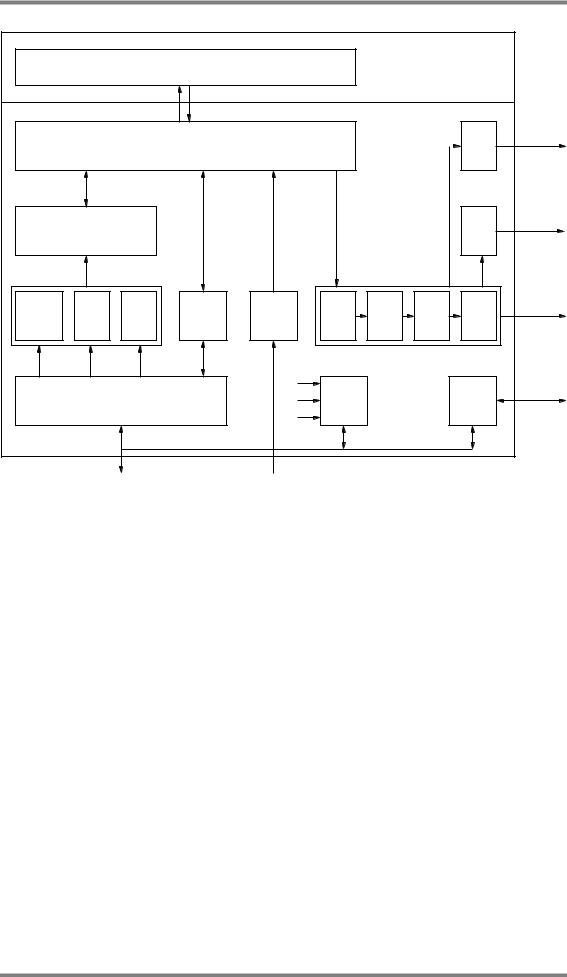
1.1Overview
The clock unit (CU) provides all necessary clocks to GDC modules and an own interface to host MCU (MB91360 series) in order to have durable access even if ULB clocks switched off.
The main functions of CU are:
•Clock source select (Oscillator, MCU Bus clock, Display clock and a reserve clock input)
•Programmable clock muliplier with APLL
•Separate dividers for master (core) clock and pixel clock
•Power management for all GDC modules
•Generation of synchronized RESET signal
•MB91360 series compliant (ULB) Bus interface for clock setup
Figure 1-1 shows the overview of the Clock Unit. OSC_IN, DIS_PIXCLK, ULB_CLK and RCLK1 are possible to use as input sources. Both clock outputs of the main unit (MASTERCLK and PIXELCLK) and two directly used clock inputs (ULB_CLK and VSC_CLKV) driving the clock gates unit which distributes to all connected GDC sub-modules.
|
|
|
OSC IN |
DIS PIXCLK |
RCLK |
ULB CLK |
VSC CLKV |
|
ULB |
|
|
|
|
|
|
|
_A |
Address Decoder |
|
|
|
|
|
|
_RDX |
|
|
|
|
|
|
|
|
|
|
|
|
|
|
|
_WRX |
|
|
|
|
|
MASTERCLK |
|
_CSX |
RSTX |
|
|
|
|
|
|
|
|
|
|
|
||
|
_CLK |
|
|
|
|
|
PIXELCLK |
|
|
Clk[Con|Pd]R_[rd|wr] |
|
Main Unit |
|
|
|
Bus |
|
ClkConR |
|
|
|
|
|
ULB |
|
|
|
|
|
|
|
Logic |
LOCK |
|
|
|
|
|
|
_D |
|
|
|
|
|
||
_A |
Register Set |
|
|
|
|
|
|
ClkPdR |
|
|
|
|
|
||
User |
|
|
|
|
|
||
_WRX |
|
|
|
|
|
||
[11] |
|
|
|
|
|||
_CLK |
|
|
|
|
|||
|
|
RSTX |
RSTX |
|
|
|
|
|
|
[15] |
|
|
|
|
|
|
|
SW_RST |
|
|
|
|
|
|
OSC_IN |
|
SYNC_RSTX_CU |
|
|
||
|
ULB_CLK |
Reset Generator |
|
|
|
|
|
|
|
|
|
|
|
|
|
|
RESETX |
|
|
|
|
|
|
SYNC_RSTX
not inverted clock outputs
Clock Gates
inverted clock outputs
PE_CLKK_OUT
MAU_CLKK_OUT
MCP_CLK_OUT K
PP_CLKK_OUT
AAF_CLKK_OUT
DIPA_CLKK_OUT
VIS_CLKK_OUT
VIS_CLKV_OUT
SDC_CLKK_OUT
CCFL_CLKK_OUT
SPB_CLKM_OUT
ULB_CLK_OUT
ULB_CLKM_OUT
GPUF_CLKK_OUT
GPUM_CLKK_OUT
GPUB_CLKK_OUT
PIX_CLKD_OUT
SPB_CLKMX_OUT
ULB_CLKKX_OUT
ULB_CLKMX_OUT
Figure 1-1: Block diagram of Clock Unit
1. MODE[3] pin is used for RCLK at Lavender
Functional Description |
Page 29 |

MB87J2120, MB87P2020-A Hardware Manual
The GDC device has four different clock domains, that means clocks derived from four different sources. The largest part of the design runs at core clock which operates at the highest frequency driven by the MASTERCLK output. Thus normally the APLL is used to provide a higher internal operation frequency. The next domain is the display output interface which operates at pixel clock frequency. For most applications
it is recommended that this is the clock from OSC_IN pin, divided by two1. So the crystal oscillator has to be choosen to have a whole-numbered multiple of the display clock frequency. Preferred routing is the DIRECT clock source channel since some displays require a small clock jitter which is not able to provide by the APLL. The other clocks for MCU interface (ULB_CLK) and video interface (VSC_CLKV) are not derived by the clock routing and generating part and used directly from the appropriate input pin.
Finally the generated source clocks of the for domains go to the clock gating/distribution module. There are gated clock buffers and inverters for each GDC module implemented. Each module has it’s own clock enable flag which can be programmed for modules needed by the application only. This method saves power of not used functional blocks of GDC (refere to table 3-1).
The configuration of CU is stored in two registers, ClkConR and ClkPdR, which are connected to User Logic Bus for writing and reading. The bus interface consists of an address decoder and circuitry for different access types (word, halfword and byte access over a 16 or 32 bit bus connection).
1.2Reset Generation
GDC works with an internally synchronized, low active reset signal. The global chip reset can be triggered by an external asynchronous reset or internally by software reset (configuration bit in ClkPdR). The external triggered RESETX results in resetting all GDC components including the Clock Unit, however software reset has no influence on CU internal registers.
Lavender synchronizes its external reset (RSTX pin). Reset is delayed until 4 clock cycles of each ULB_CLK and OSC_IN are executed. This gives stability against spikes on the RSTX line but has the disadvantage of delayed reset response of Lavender.
For Jasmine internal reset is active immediately after tying RESETX low plus a small spike filter delay. Due to the synchronization of RESETX the internal reset state ends after 4 clock periods of OSC_IN and 4 clock periods of ULB_CLK after releasing RESETX pin. Reset output RSTX_SYNC for all internal GDC register states are synchronized with OSC_IN, however internal Clock Unit registers are synchronized with ULB_CLK in addition. Thus a minimum recovery time of 4 clock cycles of OSC_IN plus 4 cycles of ULB_CLK is needed before writing to Clock Unit configuration registers is possible after RESETX becomes inactive.
The reset generator of Jasmine has a spike filter implemented, which suppresses short low pulses, typical smaller than 9 ns. Under best case operating conditions (-40 deg. C; 2.7V; fast) maximum suppressed spike width is specified to 5.5ns. This is the maximum reset pulse width which did not result in resetting the GDC device. Minimum pulse width for guaranteed reset is specified to 1 clock cycle of OSC_IN (80 ns typical).
1.3Register Set
Table 1-1 listst the clock setup registers. ClkConR (Clock Configuration Register) is mainly for generation of the base clocks and the routing/selection from one of the four input sources. It controls the clock dividers and the use of the APLL. The possibility to use a second clock path, called direct clock source, gives a high flexibility for using the APLL either for MASTERCLK or PIXELCLK generation or both. Also the pin function of DIS_PIXCLK can be defined in this register. If DIS_PIXCLK is selected as clock source the pin should be configured as an input.
Upper 8 bits of ClkConR are used as identification of the different GDC types. Lavender is identified with reading back a ’0x00’, Jasmine with a ’0x01’.
Use of DIS_PIXCLK as pixel clock output and selection of DIS_PIXCLK for the clock source can result in unintentional feedbacks and has to be avoided.
1. Preferred is an even divider value to achive 50% clock duty
Page 30
Loading...