


 Loading...
|
|
|
|
|
|
FUJITSU SEMICONDUCTOR |
|
DS07-16801-1E |
|
|
DATA SHEET |
|
|
|
|
|
|
|
|
|
|
|
|
|
|
|
|
|
|
|
|
|
|
|
32-bit Proprietary Microcontroller
CMOS
FR60Lite MB91270/280 Series
MB91F272/F272S/V280
■ DESCRIPTION
The MB91270/280 series is single chip microcontroller that builds various I/O resources and the bus control mechanisms into by using 32-bit efficient RISC CPU for the built-in control being demanded for CPU processing high performance/high-speed. Because the vast address space that 32-bit CPU accesses is supported, the external bus access is basically. To speed up CPU instruction execution, MB91270/280 has built-in RAM of 16 Kbytes (for data) .
It is best specification for the built-in usage in which efficient CPU processing power such as the digital video camera, navigation systems, and DVD players is demanded.
The MB91270/280 series power-up the bus access based on FR30/40 family CPU, and is FR60 Lite family corresponding to use at high speed.
■ FEATURES
•FR CPU characteristics
•32-bit RISC, load/store architecture with a five-stage pipeline
•Maximum operating frequency: 32 MHz (using the PLL at an oscillation frequency of 4 MHz)
•16-bit fixed length instructions (basic instructions), 1 instruction per cycle
(Continued)
■ PACKAGES
401-pin ceramic PGA |
100-pin plastic LQFP |
(PGA-401C-A02) |
(FPT-100P-M05) |

MB91270/280 Series
• Instruction optimized for embedded applications:
Memory-to-memory transfer, bit manipulation, barrel shift instruction etc.
• Instructions adapted for high - level languages:
Function entry/exit instructions, multiple - register load/store instructions
•Register interlock functions: Facilitating coding in assemblers
•Built-in multiplier supported at the instruction level. Signed 32-bit multiplication: 5 cycles.
Signed 16-bit multiplication: 3 cycles.
•Interrupt (PC, PS save): 6 cycles, 16 priority levels
•Harvard architecture allowing program access and data access to be executed simultaneously
•Instruction compatible with FR family
•External bus interface
•Maximum operating frequency: 16 MHz
•Can output full 24-bit address range (16 Mbyte space)
•8,16-bit data output
•Unused data/address pin can be used as general-purpose I/O ports.
•Capable of chip select output for completely independent four areas settable in 64 Kbytes minimum.
•Supports the following memory interfaces SRAM, ROM/Flash
•Basic bus cycle: 2 cycles
•Programmable automatic wait cycle generation function capable of inserting wait cycles for each area
•RDY input for external wait cycles
•Built-in memory
|
MB91V280 |
MB91F272 (S) |
|
|
|
ROM/Flash |
External SRAM |
Flash 256 Kbytes |
|
|
|
F-bus RAM |
48 Kbytes |
10 Kbytes |
|
|
|
The peripheral circuits are described below.
See “■PRODUCT LINEUP” for the number of available channels on each model.
•DMAC (DMA Controller)
•Capable of simultaneous operation of up to five channels
•Two forwarding factors (internal peripheral/software)
•Bit search module (for REALOS)
Search for the position of the bit “1”/“0”-changed first in one word from the MSB
•LIN UARTs (LIN-UART) : Up to 7 channels
•Asynchronous (start-stop synchronous) communications, clock synchronous communications
•Synch-Break detection
•Built-in baud rate generator on each channel
•Supports SPI (mode 2: Clock synchronous communication mode)
•CAN CONTROLLERS : 3 channels (Max)
•High-speed transfer : 1 Mbps
•32 message buffer (128 message buffer on the MB91V280)
(Continued)
2

MB91270/280 Series
•Various timers
•16-bit reload timer : 3 channels (including one channel for use by REALOS) The internal clock can be divided by 2, 8, or 32
•16-bit free-running timer: 4 channels Output compare module: 8 channels Input capture module: 8 channels
•8/16-bit PPG timer: 8-bit x 16 channels or 16-bit x 8 channels
•Interrupt controller
•Interrupt from internal peripheral
•Software-selectable priority level (16 levels)
•D/A converter : 2 channels
8-bit or 10-bit resolution, R-2R type
•A/D converter: 24 channels (MB91V280 has an additional module with eight more channels)
•10-bit resolution
•Successive approximation conversion type Conversion time : 3 µs
•Conversion mode (single conversion mode, continuous conversion mode)
•Activation source (software, external trigger, peripheral interrupt)
•Other interval timer/counter
•8/16-bit up down counter :
8 bits × 4 channels or 16 bits × 2 channels
•16-bit timebase timer / watchdog timer
•I2C bus interface* (400 Kbps): 3 channels
•Master/slave sending and receiving
•Arbitration and clock synchronization
•Hardware watchdog
Interval time: 569 ms (Min), 771 ms (Max)
(Using a self-oscillation circuit (100 kHz) with a trimming function.)
•I/O port
•Pull-up/pull-down can be controlled independently for each pin.
•The input level for each pin can be set to either CMOS Schmitt trigger levels or CMOS automotive Schmitt trigger levels.
•The pin level can be read directly.
•Max 120 ports
•Other features
•Internal oscillator circuit as clock source, allowing PLL multiplication to be selected
•INITX is prepared as a reset pin.
•Watchdog timer reset, software reset
•Available low-power consumption modes are stop mode, sleep mode, and real time clock mode. Supports low-power consumption operation with CPU operating at 32 kHz (MB91F272 only).
•Gear function
•Built-in timebase timer
•Output clock (clock monitor)
(Continued)
3

MB91270/280 Series
(Continued)
•Clock Modulator
•Clock monitor function
Uses an internal self-oscillation circuit to monitor whether the main clock halts.
• Package |
PGA-401, LQFP-100 |
•CMOS technology (0.35 m)
•Power supply voltage: 3.5 V to 5.5 V
The 3.3 V supply to internal circuits is generated by an internal step-down circuit.
*: I2C license
Purchase of Fujitsu I2C components conveys a license under the Philips I2C Patent Rights to use, these components in an I2C system provided that the system conforms to the I2C Standard Specification as defined by Philips.
4

MB91270/280 Series
■ PRODUCT LINEUP
|
Kind |
MB91F272 (S) |
MB91V280 |
Parameter |
|
||
|
|
|
|
|
|
|
|
Package |
|
LQFP-100 |
PGA-401 |
|
|
|
|
Built - in ROM/Flash |
|
Flash 256 Kbytes |
External SRAM |
|
|
|
|
RAM |
|
10 Kbytes |
48 Kbytes |
|
|
|
|
|
|
Address : 24 bits |
Address : 24 bits |
External bus |
|
Data : 16 bits |
|
|
Data : 16 bits |
||
|
|
(Multiplex only) |
|
|
|
|
|
|
|
|
|
External interrupt |
|
16 channels |
40 channels |
|
|
|
|
DMAC (DMA Controller) |
|
5 channels |
5 channels |
|
|
|
|
Clock modulator |
|
Yes |
Yes |
|
|
|
|
Clock monitor function |
|
Yes |
Yes |
|
|
|
|
Clock monitor |
|
Yes |
Yes |
|
|
|
|
32 kHz sub-clock |
|
Option |
Yes |
|
(MB91F272 only) |
||
|
|
|
|
|
|
|
|
Real time clock |
|
Yes |
Yes |
|
|
|
|
CAN controllers |
|
1 channel (32 message buffer) |
3 channels (128 message buffer) |
|
|
|
|
LIN UARTs (LIN-UART) |
|
7 channels |
7 channels |
|
|
|
|
I2C interface |
|
3 channels |
3 channels |
16 - bit reload timer |
|
3 channels |
3 channels |
|
|
|
|
8/16-bit up down counter |
|
2 channels |
2 channels |
|
|
|
|
16 - bit free - run timer |
|
4 channels |
4 channels |
|
|
|
|
Input capture |
|
8 channels |
8 channels |
|
|
|
|
Output compare |
|
8 channels |
8 channels |
|
|
|
|
8/16-bit PPG |
|
16-bit x 8 channels |
16-bit x 8 channels |
|
8-bit x 16 channels |
8-bit x 16 channels |
|
|
|
||
|
|
|
|
10-bit A/D converter |
|
24 channels |
24 channels + 8 channels |
|
|
|
|
8/10-bit D/A converter |
|
No |
2 channels |
|
|
|
|
Pin pull-up/down |
|
See “■PIN FUNCTION” |
All pins |
|
|
|
|
Input level selector |
|
See “■PIN FUNCTION” |
All pins |
|
|
|
|
Debugging support |
|
Wild register |
DSU4 |
|
|
|
|
5
MB91270/280 Series
■ PIN ASSIGNMENT
(TOP VIEW)
P26/A22/IN2 1
P27/A23/IN3 2
P30/ASX/IN4 3
P31/RDX/IN5 4 P32/WR0X/RX2/INT10R 5 P33/WR1X/TX2 6 P34/BRQ/OUT4 7 P35/BGRNTX/OUT5 8 P36/RDY/OUT6 9 P37/SYSCLK/OUT7 10 P40/(X0A) 11 P41/(X1A) 12
VCC 13
VSS 14
C 15 P42/IN6/RX1/INT9R 16 P43/IN7/TX1 17 P44/SDA0/FRCK0 18 P45/AIN2/SCL0/FRCK1 19 P46/BIN2/SDA1 20 P47/ZIN2/SCL1 21 P50/AN8/SIN2 22 P51/AN9/SOT2 23 P52/AN10/SCK2 24 P53/AN11/BIN1 25
P25/A21/IN1 |
P24/A20/IN0 |
P23/A19/PPGF |
P22/A18/PPGD |
P21/A17/PPGB |
P20/A16/PPG9 |
P17/AD15/SCK4 |
P16/AD14/SOT4 |
P15/AD13/SIN4 |
X0 |
X1 |
VSS |
VCC |
P14/AD12/SCK3 |
P13/AD11/SOT3 |
P12/AD10/SIN3/INT11R |
P11/AD09/TOT1 |
P10/AD08/TIN1 |
P07/AD07/INT15 |
P06/AD06/INT14 |
P05/AD05/SCK6/INT13 |
P04/AD04/SOT6/INT12 |
P03/AD03/SIN6/INT11 |
P02/AD02/SCK5/INT10 |
P01/AD01/SOT5/INT9 |
|
|
|
|
|
|
|
|
|
|
|
|
|
|
|
|
|
|
|
|
|
|
|
|
|
100 |
99 |
98 |
97 |
96 |
95 |
94 |
93 |
92 |
91 |
90 |
89 |
88 |
87 |
86 |
85 |
84 |
83 |
82 |
81 |
80 |
79 |
78 |
77 |
76 |
LQFP-100
26 |
27 |
28 |
29 |
30 |
31 |
32 |
33 |
34 |
35 |
36 |
37 |
38 |
39 |
40 |
41 |
42 |
43 |
44 |
45 |
46 |
47 |
48 |
49 |
50 |
|
|
|
|
|
|
|
|
|
|
|
|
|
|
|
|
|
|
|
|
|
|
|
|
|
P54/AN12/AIN1 |
P55/AN13/ZIN1 |
P56/AN14 |
P57/AN15 |
AVCC |
AVRH |
AVRL |
AVSS |
P60/AN0/PPG0 |
P61/AN1/PPG2 |
P62/AN2/PPG4 |
P63/AN3/PPG6 |
P64/AN4/PPG8 |
P65/AN5/PPGA |
P66/AN6/PPGC |
P67/AN7/PPGE |
VSS |
P70/AN16/INT0 |
P71/AN17/INT1 |
P72/AN18/INT2 |
P73/AN19/INT3 |
P74/AN20/INT4 |
P75/AN21/INT5 |
MD2 |
MD1 |
75 |
P00/AD00/SIN5/INT8 |
74 |
PA1/TX0 |
73 |
PA0/RX0/INT8R |
72 |
P97/OUT3 |
71 |
P96/OUT2/ZIN0 |
70 |
P95/OUT1/BIN0 |
69 |
P94/OUT0/AIN0 |
68 |
P93/PPG7/ZIN3/CS3X |
67 |
P92/PPG5/BIN3/CS2X |
66 |
P91/PPG3/AIN3/CS1X |
65 |
P90/PPG1/CS0X |
64 |
VSS |
63 |
VCC |
62 |
P87/SCK1 |
61 |
P86/SOT1 |
60 |
P85/SIN1 |
59 |
P84/SCK0/INT15R |
58 |
P83/TOT2/SOT0 |
57 |
P82/TIN2/SIN0/INT14R |
56 |
P81/TOT0/INT13R/CKOT |
55 |
P80/TIN0/INT12R/ADTG |
54 |
P77/AN23/INT7/SCL2 |
53 |
P76/AN22/INT6/SDA2 |
52 |
INITX |
51 |
MD0 |
(FPT-100P-M05)
6

MB91270/280 Series
■ PIN FUNCTION
Pin No. |
Pin name |
Function |
I/O circuit |
Function |
|
name |
type* |
||||
|
|
|
|||
|
|
|
|
|
|
90 |
X1 |
X1 |
OB |
Oscillator output pin |
|
|
|
|
|
|
|
91 |
X0 |
X0 |
OA |
Oscillator input pin |
|
|
|
|
|
|
|
52 |
INITX |
INITX |
N |
Reset input pin (“L” active) |
|
|
|
|
|
|
|
49 to 51 |
MD2 to MD0 |
MD2 to MD0 |
J |
Operation mode select input pin. |
|
Connect to VCC or VSS directly. |
|||||
|
|
|
|
||
|
|
|
|
|
|
|
|
|
|
Port 0 |
|
|
|
|
|
|
|
|
|
P00 |
|
General-purpose I/O ports. |
|
|
|
|
This function is enabled in single-chip mode. |
||
|
|
|
|
||
|
|
|
|
|
|
75 |
P00/AD00/ |
AD00 |
T |
External address/data bus I/O pin bit 0 |
|
SIN5/INT8 |
This function is enabled when the external bus is enabled. |
||||
|
|
|
|||
|
|
INT8 |
|
External interrupt request 8 input pin |
|
|
|
|
|
|
|
|
|
SIN5 |
|
Serial data input pin for LIN-UART5 |
|
|
|
|
|
|
|
|
|
P01 |
|
General-purpose I/O ports. |
|
|
|
|
This function is enabled in single-chip mode. |
||
|
|
|
|
||
|
|
|
|
|
|
76 |
P01/AD01/ |
AD01 |
T |
External address/data bus I/O pin bit 1 |
|
SOT5/INT9 |
This function is enabled when the external bus is enabled. |
||||
|
|
|
|||
|
|
INT9 |
|
External interrupt request 9 input pin |
|
|
|
|
|
|
|
|
|
SOT5 |
|
Serial data output pin for LIN-UART5 |
|
|
|
|
|
|
|
|
|
P02 |
|
General-purpose I/O ports. |
|
|
|
|
This function is enabled in single-chip mode. |
||
|
|
|
|
||
|
|
|
|
|
|
77 |
P02/AD02/ |
AD02 |
T |
External address/data bus I/O pin bit 2 |
|
SCK5/INT10 |
This function is enabled when the external bus is enabled. |
||||
|
|
|
|||
|
|
INT10 |
|
External interrupt request 10 input pin |
|
|
|
|
|
|
|
|
|
SCK5 |
|
Clock I/O pin for LIN-UART5 |
|
|
|
|
|
|
|
|
|
P03 |
|
General-purpose I/O ports. |
|
|
|
|
This function is enabled in single-chip mode. |
||
|
|
|
|
||
|
|
|
|
|
|
78 |
P03/AD03/ |
AD03 |
T |
External address/data bus I/O pin bit 3 |
|
SIN6/INT11 |
This function is enabled when the external bus is enabled. |
||||
|
|
|
|||
|
|
INT11 |
|
External interrupt request 11 input pin |
|
|
|
|
|
|
|
|
|
SIN6 |
|
Serial data input pin for LIN-UART6 |
|
|
|
|
|
|
|
|
|
P04 |
|
General-purpose I/O ports. |
|
|
|
|
This function is enabled in single-chip mode. |
||
|
|
|
|
||
|
|
|
|
|
|
79 |
P04/AD04/ |
AD04 |
T |
External address/data bus I/O pin bit 4 |
|
SOT6/INT12 |
This function is enabled when the external bus is enabled. |
||||
|
|
|
|||
|
|
INT12 |
|
External interrupt request 12 input pin |
|
|
|
|
|
|
|
|
|
SOT6 |
|
Serial data output pin for LIN-UART6 |
|
|
|
|
|
|
* : See “■ I/O CIRCUIT TYPE” for the I/O circuit type.
(Continued)
7

MB91270/280 Series
|
|
|
|
|
|
|
|
|
|
|
|
|
|
|
|
|
Pin No. |
Pin name |
Function |
I/O circuit |
|
Function |
|
|
name |
type* |
|
|
|||
|
|
|
|
|
|
||
|
|
|
|
|
|
|
|
|
|
|
P05 |
|
|
General-purpose I/O ports. |
|
|
|
|
|
|
This function is enabled in single-chip mode. |
|
|
|
|
|
|
|
|
|
|
|
|
|
|
|
|
|
|
|
80 |
P05/AD05/ |
AD05 |
T |
|
External address/data bus I/O pin bit 5 |
|
|
SCK6/INT13 |
|
This function is enabled when the external bus is enabled. |
|
|||
|
|
|
|
|
|
||
|
|
|
|
|
|
|
|
|
|
|
INT13 |
|
|
External interrupt request 13 input pin |
|
|
|
|
|
|
|
|
|
|
|
|
SCK6 |
|
|
Clock I/O pin for LIN-UART6 |
|
|
|
|
|
|
|
|
|
|
|
|
P06 |
|
|
General-purpose I/O ports. |
|
|
|
|
|
|
This function is enabled in single-chip mode. |
|
|
|
|
P06/AD06/ |
|
|
|
|
|
|
|
|
|
|
|
|
|
|
81 |
|
T |
|
External address/data bus I/O pin bit 6 |
|
|
|
INT14 |
AD06 |
|
|
|||
|
|
|
|
This function is enabled when the external bus is enabled. |
|
||
|
|
|
|
|
|
|
|
|
|
|
|
|
|
|
|
|
|
|
INT14 |
|
|
External interrupt request 14 input pin |
|
|
|
|
|
|
|
|
|
|
|
|
P07 |
|
|
General-purpose I/O ports. |
|
|
|
|
|
|
This function is enabled in single-chip mode. |
|
|
|
|
P07/AD07/ |
|
|
|
|
|
|
|
|
|
|
|
|
|
|
82 |
|
T |
|
External address/data bus I/O pin bit 7 |
|
|
|
INT15 |
AD07 |
|
|
|||
|
|
|
|
This function is enabled when the external bus is enabled. |
|
||
|
|
|
|
|
|
|
|
|
|
|
|
|
|
|
|
|
|
|
INT15 |
|
|
External interrupt request 15 input pin |
|
|
|
|
|
|
|
|
|
|
|
|
|
|
Port 1 |
|
|
|
|
|
|
|
|
|
|
|
|
|
P10 |
|
|
General-purpose I/O ports. |
|
|
|
|
|
|
This function is enabled in single-chip mode. |
|
|
|
|
P10/AD08/ |
|
|
|
|
|
|
|
|
|
|
|
|
|
|
83 |
|
T |
|
External address/data bus I/O pin bit 8 |
|
|
|
TIN1 |
AD08 |
|
|
|||
|
|
|
|
This function is enabled when the external bus is enabled. |
|
||
|
|
|
|
|
|
|
|
|
|
|
|
|
|
|
|
|
|
|
TIN1 |
|
|
Event input pin for reload timer 1 |
|
|
|
|
|
|
|
|
|
|
|
|
P11 |
|
|
General-purpose I/O ports. |
|
|
|
|
|
|
This function is enabled in single-chip mode. |
|
|
|
|
P11/AD09/ |
|
|
|
|
|
|
|
|
|
|
|
|
|
|
84 |
|
T |
|
External address/data bus I/O pin bit 9 |
|
|
|
TOT1 |
AD09 |
|
|
|||
|
|
|
|
This function is enabled when the external bus is enabled. |
|
||
|
|
|
|
|
|
|
|
|
|
|
|
|
|
|
|
|
|
|
TOT1 |
|
|
Output pin for reload timer 1 |
|
|
|
|
|
|
|
|
|
|
|
|
P12 |
|
|
General-purpose I/O ports. |
|
|
|
|
|
|
This function is enabled in single-chip mode. |
|
|
|
|
|
|
|
|
|
|
|
|
P12/AD10/ |
|
|
|
|
|
|
|
AD10 |
|
|
External address/data bus I/O pin bit 10 |
|
|
|
85 |
SIN3/ |
T |
|
|
||
|
|
This function is enabled when the external bus is enabled. |
|
||||
|
|
INT11R |
|
|
|
|
|
|
|
|
|
|
|
|
|
|
|
SIN3 |
|
|
Serial data input pin for LIN-UART3 |
|
|
|
|
|
|
|
|
||
|
|
|
|
|
|
|
|
|
|
|
INT11R |
|
|
External interrupt request 11 input pin (Set by EISSR) |
|
|
|
|
|
|
|
|
|
|
|
|
P13 |
|
|
General-purpose I/O ports. |
|
|
|
|
|
|
This function is enabled in single-chip mode. |
|
|
|
|
P13/AD11/ |
|
|
|
|
|
|
|
|
|
|
|
|
|
|
86 |
AD11 |
T |
|
External address/data bus I/O pin bit 11 |
|
|
|
SOT3 |
|
|
||||
|
|
|
|
This function is enabled when the external bus is enabled. |
|
||
|
|
|
|
|
|
|
|
|
|
|
|
|
|
|
|
|
|
|
SOT3 |
|
|
Serial data output pin for LIN-UART3 |
|
|
|
|
|
|
|
|
|
* : See “■ I/O CIRCUIT TYPE” for the I/O circuit type.
(Continued)
8

MB91270/280 Series
|
|
|
|
|
|
|
|
|
|
|
|
|
|
|
Pin No. |
Pin name |
Function |
I/O circuit |
Function |
|
|
name |
type* |
|
|||
|
|
|
|
|
||
|
|
|
|
|
|
|
|
|
|
P14 |
|
General-purpose I/O ports. |
|
|
|
|
|
This function is enabled in single-chip mode. |
|
|
|
|
P14/AD12/ |
|
|
|
|
|
87 |
|
T |
|
|
|
|
|
External address/data bus I/O pin bit 12 |
|
|||
|
SCK3 |
AD12 |
|
|||
|
|
|
This function is enabled when the external bus is enabled. |
|
||
|
|
|
|
|
|
|
|
|
|
|
|
|
|
|
|
|
SCK3 |
|
Clock I/O pin for LIN-UART3 |
|
|
|
|
|
|
|
|
|
|
|
P15 |
|
General-purpose I/O ports. |
|
|
|
|
|
This function is enabled in single-chip mode. |
|
|
|
|
P15/AD13/ |
|
|
|
|
|
|
|
|
|
|
|
|
92 |
|
T |
External address/data bus I/O pin bit 13 |
|
|
|
SIN4 |
AD13 |
|
|||
|
|
|
This function is enabled when the external bus is enabled. |
|
||
|
|
|
|
|
|
|
|
|
|
|
|
|
|
|
|
|
SIN4 |
|
Serial data input pin for LIN-UART4 |
|
|
|
|
|
|
|
|
|
|
|
P16 |
|
General-purpose I/O ports. |
|
|
|
|
|
This function is enabled in single-chip mode. |
|
|
|
|
P16/AD14/ |
|
|
|
|
|
|
|
|
|
|
|
|
93 |
|
T |
External address/data bus I/O pin bit 14 |
|
|
|
SOT4 |
AD14 |
|
|||
|
|
|
This function is enabled when the external bus is enabled. |
|
||
|
|
|
|
|
|
|
|
|
|
|
|
|
|
|
|
|
SOT4 |
|
Serial data output pin for LIN-UART4 |
|
|
|
|
|
|
|
|
|
|
|
P17 |
|
General-purpose I/O ports. |
|
|
|
|
|
This function is enabled in single-chip mode. |
|
|
|
|
P17/AD15/ |
|
|
|
|
|
|
|
|
|
|
|
|
94 |
|
T |
External address/data bus I/O pin bit 15 |
|
|
|
SCK4 |
AD15 |
|
|||
|
|
|
This function is enabled when the external bus is enabled. |
|
||
|
|
|
|
|
|
|
|
|
|
|
|
|
|
|
|
|
SCK4 |
|
Clock I/O pin for LIN-UART4 |
|
|
|
|
|
|
|
|
|
|
|
|
|
Port 2 |
|
|
|
|
|
|
|
|
|
|
|
P20 |
|
General-purpose I/O ports. |
|
|
|
|
|
This function is enabled in single-chip mode. |
|
|
|
|
P20/A16/ |
|
|
|
|
|
|
|
|
|
|
|
|
95 |
|
A |
External address bus output pin bit 16 |
|
|
|
PPG9 |
A16 |
|
|||
|
|
|
This function is enabled when the external bus is enabled. |
|
||
|
|
|
|
|
|
|
|
|
|
|
|
|
|
|
|
|
PPG9 |
|
Output pin for PPG9 |
|
|
|
|
|
|
|
|
|
|
|
P21 |
|
General-purpose I/O ports. |
|
|
|
|
|
This function is enabled in single-chip mode. |
|
|
|
|
P21/A17/ |
|
|
|
|
|
|
|
|
|
|
|
|
96 |
|
A |
External address bus output pin bit 17 |
|
|
|
PPGB |
A17 |
|
|||
|
|
|
This function is enabled when the external bus is enabled. |
|
||
|
|
|
|
|
|
|
|
|
|
|
|
|
|
|
|
|
PPGB |
|
Output pin for PPGB |
|
|
|
|
|
|
|
|
|
|
|
P22 |
|
General-purpose I/O ports. |
|
|
|
|
|
This function is enabled in single-chip mode. |
|
|
|
|
P22/A18/ |
|
|
|
|
|
|
|
|
|
|
|
|
97 |
|
A |
External address bus output pin bit 18 |
|
|
|
PPGD |
A18 |
|
|||
|
|
|
This function is enabled when the external bus is enabled. |
|
||
|
|
|
|
|
|
|
|
|
|
|
|
|
|
|
|
|
PPGD |
|
Output pin for PPGD |
|
|
|
|
|
|
|
|
* : See “■ I/O CIRCUIT TYPE” for the I/O circuit type.
(Continued)
9

MB91270/280 Series
|
|
|
|
|
|
|
|
|
|
|
|
|
|
|
Pin No. |
Pin name |
Function |
I/O circuit |
Function |
|
|
name |
type* |
|
|||
|
|
|
|
|
||
|
|
|
|
|
|
|
|
|
|
P23 |
|
General-purpose I/O ports. |
|
|
|
|
|
This function is enabled in single-chip mode. |
|
|
|
|
P23/A19/ |
|
|
|
|
|
98 |
|
A |
|
|
|
|
|
External address bus output pin bit 19 |
|
|||
|
PPGF |
A19 |
|
|||
|
|
|
This function is enabled when the external bus is enabled. |
|
||
|
|
|
|
|
|
|
|
|
|
|
|
|
|
|
|
|
PPGF |
|
Output pin for PPGF |
|
|
|
|
|
|
|
|
|
|
|
P24 to P27 |
|
General-purpose I/O ports. |
|
|
|
P24/A20/IN0 |
|
This function is enabled in single-chip mode. |
|
|
|
99, 100, |
|
|
|
||
|
|
|
|
|
||
|
|
A |
External address bus output pin bits 20 to 23 |
|
||
|
1, 2 |
to |
A20 to A23 |
|
||
|
P27/A23/IN3 |
|
This function is enabled when the external bus is enabled. |
|
||
|
|
|
|
|
|
|
|
|
|
IN0 to IN3 |
|
Data sample input pins for input capture ICU0 to ICU3 |
|
|
|
|
|
|
|
|
|
|
|
|
|
Port 3 |
|
|
|
|
|
|
|
|
|
|
|
P30 |
|
General-purpose I/O ports. |
|
|
|
|
|
This function is enabled in single-chip mode. |
|
|
|
|
P30/ASX/ |
|
|
|
|
|
|
|
|
|
|
|
|
3 |
|
A |
External address strobe output pin |
|
|
|
IN4 |
ASX |
|
|||
|
|
|
This function is enabled when the external bus is enabled. |
|
||
|
|
|
|
|
|
|
|
|
|
|
|
|
|
|
|
|
IN4 |
|
Data sample input pin for input capture ICU4 |
|
|
|
|
|
|
|
|
|
|
|
P31 |
|
General-purpose I/O ports. |
|
|
|
|
|
This function is enabled in single-chip mode. |
|
|
|
|
P31/RDX/ |
|
|
|
|
|
|
|
|
|
|
|
|
4 |
|
A |
External read strobe output pin |
|
|
|
IN5 |
RDX |
|
|||
|
|
|
This function is enabled when the external bus is enabled. |
|
||
|
|
|
|
|
|
|
|
|
|
|
|
|
|
|
|
|
IN5 |
|
Data sample input pin for input capture ICU5 |
|
|
|
|
|
|
|
|
|
|
|
P32 |
|
General-purpose I/O ports. |
|
|
|
|
|
This function is enabled in single-chip mode. |
|
|
|
|
|
|
|
|
|
|
|
|
|
|
|
|
|
|
P32/WR0X/ |
|
|
External data bus write strobe output pin. Enabled when the |
|
|
|
WR0X |
|
external bus is enabled. |
|
|
|
5 |
RX2/ |
A |
|
||
|
WR0X is used as the data write strobe for 8-bit access and |
|
||||
|
|
INT10R |
|
|
|
|
|
|
|
|
as the upper 8 bits of the data in 16-bit access. |
|
|
|
|
|
|
|
|
|
|
|
|
|
|
|
|
|
|
|
RX2 |
|
CAN2 RX input pin (MB91V280 only) |
|
|
|
|
|
|
|
|
|
|
|
INT10R |
|
External interrupt request 10 input pin (Set by EISSR) |
|
|
|
|
|
|
|
|
|
|
|
P33 |
|
General-purpose I/O ports. |
|
|
|
|
|
This function is enabled in single-chip mode. |
|
|
|
|
P33/WR1X/ |
|
|
|
|
|
|
|
|
|
|
|
|
|
|
|
Write strobe output pin for lower 8 bits in external data bus |
|
|
|
6 |
TX2 |
|
A |
|
|
|
WR1X |
Enabled when the external bus is enabled and external bus |
|
|||
|
|
|
|
|
||
|
|
|
|
|
16-bit mode is selected. |
|
|
|
|
|
|
|
|
|
|
|
TX2 |
|
CAN2 TX output pin (MB91V280 only) |
|
|
|
|
|
|
|
|
* : See “■ I/O CIRCUIT TYPE” for the I/O circuit type.
(Continued)
10
MB91270/280 Series
|
|
|
|
|
|
|
|
|
|
|
|
|
|
|
Pin No. |
Pin name |
Function |
I/O circuit |
Function |
|
|
name |
type* |
|
|||
|
|
|
|
|
||
|
|
|
|
|
|
|
|
|
|
P34 |
|
General-purpose I/O ports. |
|
|
|
|
|
This function is enabled in single-chip mode. |
|
|
|
|
|
|
|
|
|
|
|
|
|
|
|
|
|
|
P34/BRQ/ |
|
T |
External bus request input pin |
|
|
7 |
|
Enabled when the external bus and the bus request func- |
|
||
|
OUT4 |
BRQ |
(A) |
|
||
|
|
tions are enabled. |
|
|||
|
|
|
|
|
|
|
|
|
|
|
|
(MB91V280 only) |
|
|
|
|
|
|
|
|
|
|
|
OUT4 |
|
Waveform output pin for output compare OCU4. |
|
|
|
|
|
|
|
|
|
|
|
P35 |
|
General-purpose I/O ports. |
|
|
|
|
|
This function is enabled in single-chip mode. |
|
|
|
|
|
|
|
|
|
|
|
|
|
|
|
|
|
|
P35/ |
|
|
External bus acknowledge output pin |
|
|
8 |
BGRNTX/ |
BGRNTX |
A |
Enabled when the external bus and the bus request |
|
|
|
OUT5 |
|
functions are enabled. |
|
|
|
|
|
|
|
||
|
|
|
|
|
(MB91V280 only) |
|
|
|
|
|
|
|
|
|
|
|
OUT5 |
|
Waveform output pin for output compare OCU5. |
|
|
|
|
|
|
|
|
|
|
|
P36 |
|
General-purpose I/O ports. |
|
|
|
|
|
This function is enabled in single-chip mode. |
|
|
|
|
|
|
|
|
|
|
|
|
|
|
|
|
|
9 |
P36/RDY/ |
|
T |
External ready input pin |
|
|
OUT6 |
RDY |
Enabled when the external bus and the bus request func- |
|
||
|
|
|
|
|||
|
|
|
|
|
tions are enabled. |
|
|
|
|
|
|
|
|
|
|
|
OUT6 |
|
Waveform output pin for output compare OCU6. |
|
|
|
|
|
|
|
|
|
|
|
P37 |
|
General-purpose I/O ports. |
|
|
|
P37/ |
|
This function is enabled in single-chip mode. |
|
|
|
|
|
|
|
||
|
|
|
|
|
|
|
|
10 |
SYSCLK/ |
SYSCLK |
A |
External clock output pin |
|
|
|
OUT7 |
|
This function is enabled when the external bus is enabled. |
|
|
|
|
|
|
|
||
|
|
|
|
|
|
|
|
|
|
OUT7 |
|
Waveform output pin for output compare OCU7. |
|
|
|
|
|
|
|
|
|
|
|
|
|
Port 4 |
|
|
|
|
|
|
|
|
|
|
|
P40, P41 |
A |
General-purpose I/O ports |
|
|
|
P40/ (X0A) , |
(S-suffix models) |
|
||
|
11, 12 |
|
|
|
||
|
P41/ (X1A) |
|
|
|
|
|
|
X0A, X1A |
WA |
sub-clock oscillator input pin |
|
||
|
|
|
||||
|
|
|
WB |
(without S-suffix models) |
|
|
|
|
|
|
|
||
|
|
|
|
|
|
|
|
|
|
P42 |
|
General-purpose I/O ports |
|
|
|
|
|
|
|
|
|
16 |
P42/IN6/ |
IN6 |
A |
Data sample input pin for input capture ICU6 |
|
|
RX1/INT9R |
|
|
|
||
|
RX1 |
CAN1 RX input pin (MB91V280 only) |
|
|||
|
|
|
|
|||
|
|
|
|
|
|
|
|
|
|
INT9R |
|
External interrupt request 9 input pin (Set by EISSR) |
|
|
|
|
|
|
|
|
|
|
P43/IN7/ |
P43 |
|
General-purpose I/O ports |
|
|
17 |
|
|
|
|
|
|
IN7 |
A |
Data sample input pin for input capture ICU7 |
|
||
|
TX1 |
|
||||
|
|
|
|
|
|
|
|
|
|
TX1 |
|
CAN1 TX output pin (MB91V280 only) |
|
|
|
|
|
|
|
|
|
|
P44/SDA0/ |
P44 |
|
General-purpose I/O ports |
|
|
|
|
|
|
|
|
|
18 |
SDA0 |
C |
Serial data I/O pin for I2C0 |
|
|
|
FRCK0 |
|
||||
|
|
|
FRCK0 |
|
16-bit input/output timer 0 input pin |
|
|
|
|
|
|
|
|
* : See “■ I/O CIRCUIT TYPE” for the I/O circuit type.
(Continued)
11

MB91270/280 Series
|
|
|
|
|
|
|
|
|
|
|
|
|
|
|
Pin No. |
Pin name |
Function |
I/O circuit |
Function |
|
|
name |
type* |
|
|||
|
|
|
|
|
||
|
|
|
|
|
|
|
|
|
|
P45 |
|
General-purpose I/O ports |
|
|
|
P45/AIN2/ |
|
|
|
|
|
|
SCL0 |
|
Serial clock I/O pin for I2C0 |
|
|
|
19 |
SCL0/ |
|
C |
|
|
|
FRCK1 |
16-bit input/output timer 1 input pin |
|
|||
|
|
FRCK1 |
|
|
||
|
|
|
|
|
|
|
|
|
|
AIN2 |
|
16/8-bit up-count input pin for up down counter 2/3 |
|
|
|
|
|
|
|
|
|
|
P46/BIN2/ |
P46 |
|
General-purpose I/O ports |
|
|
|
|
|
|
|
|
|
20 |
SDA1 |
C |
Serial clock I/O pin for I2C1 |
|
|
|
SDA1 |
|
||||
|
|
|
BIN2 |
|
16/8-bit down-count input pin for up down counter 2/3 |
|
|
|
|
|
|
|
|
|
|
P47/ZIN2/ |
P47 |
|
General-purpose I/O ports |
|
|
|
|
|
|
|
|
|
21 |
SCL1 |
C |
Serial clock I/O pin for I2C1 |
|
|
|
SCL1 |
|
||||
|
|
|
ZIN2 |
|
16/8-bit reset input pin for up down counter 2/3 |
|
|
|
|
|
|
|
|
|
|
|
|
|
Port 5 |
|
|
|
|
|
|
|
|
|
|
P50/AN8/ |
P50 |
|
General-purpose I/O ports |
|
|
|
|
|
|
|
|
|
22 |
AN8 |
D |
Analog input pin of A/D converter |
|
|
|
SIN2 |
|
||||
|
|
|
|
|
|
|
|
|
|
SIN2 |
|
Serial data input pin for LIN-UART2 |
|
|
|
|
|
|
|
|
|
|
P51/AN9/ |
P51 |
|
General-purpose I/O ports |
|
|
|
|
|
|
|
|
|
23 |
AN9 |
D |
Analog input pin of A/D converter |
|
|
|
SOT2 |
|
||||
|
|
|
|
|
|
|
|
|
|
SOT2 |
|
Serial data output pin for LIN-UART2 |
|
|
|
|
|
|
|
|
|
|
P52/AN10/ |
P52 |
|
General-purpose I/O ports |
|
|
|
|
|
|
|
|
|
24 |
AN10 |
D |
Analog input pin of A/D converter |
|
|
|
SCK2 |
|
||||
|
|
|
|
|
|
|
|
|
|
SCK2 |
|
Clock I/O pin for LIN-UART2 |
|
|
|
|
|
|
|
|
|
|
P53/AN11/ |
P53 |
|
General-purpose I/O ports |
|
|
|
|
|
|
|
|
|
25 |
AN11 |
D |
Analog input pin of A/D converter |
|
|
|
BIN1 |
|
||||
|
|
|
|
|
|
|
|
|
|
BIN1 |
|
8-bit down-count input pin for 16-bit up down counter 1 |
|
|
|
|
|
|
|
|
|
|
P54/AN12/ |
P54 |
|
General-purpose I/O ports |
|
|
|
|
|
|
|
|
|
26 |
AN12 |
D |
Analog input pin of A/D converter |
|
|
|
AIN1 |
|
||||
|
|
|
|
|
|
|
|
|
|
AIN1 |
|
8-bit up-count input pin for 16-bit up down counter 1 |
|
|
|
|
|
|
|
|
|
|
P55/AN13/ |
P55 |
|
General-purpose I/O ports |
|
|
|
|
|
|
|
|
|
27 |
AN13 |
D |
Analog input pin of A/D converter |
|
|
|
ZIN1 |
|
||||
|
|
|
|
|
|
|
|
|
|
ZIN1 |
|
8-bit reset input pin for 16-bit up down counter 1 |
|
|
|
|
|
|
|
|
|
|
P56/AN14/ |
P56 |
|
General-purpose I/O ports |
|
|
|
|
|
|
|
|
|
28 |
DAO0 |
AN14 |
E |
Analog input pin of A/D converter |
|
|
|
|
|
|
|
|
|
|
|
DAO0 |
|
Analog output pin 0 for D/A converter (MB91V280 only) |
|
|
|
|
|
|
|
|
|
|
P57/AN15/ |
P57 |
|
General-purpose I/O ports |
|
|
|
|
|
|
|
|
|
29 |
AN15 |
E |
Analog input pin of A/D converter |
|
|
|
DAO1 |
|
||||
|
|
|
|
|
|
|
|
|
|
DAO1 |
|
Analog output pin 1 for D/A converter (MB91V280 only) |
|
|
|
|
|
|
|
|
* : See “■ I/O CIRCUIT TYPE” for the I/O circuit type.
(Continued)
12

MB91270/280 Series
|
|
|
|
|
|
|
|
|
|
|
|
|
|
|
Pin No. |
Pin name |
Function |
I/O circuit |
Function |
|
|
name |
type* |
|
|||
|
|
|
|
|
||
|
|
|
|
|
|
|
|
|
|
|
|
Port 6 |
|
|
|
|
|
|
|
|
|
|
|
P60 to P67 |
|
General-purpose I/O ports |
|
|
|
|
|
|
|
|
|
|
|
AN0 to AN7 |
|
Analog input pin of A/D converter |
|
|
|
|
|
|
|
|
|
|
P60/AN0/ |
PPG0 |
|
|
|
|
|
PPG0 |
PPG2 |
|
|
|
|
34 to 41 |
to |
PPG4 |
D |
|
|
|
|
P67/AN7/ |
PPG6 |
|
Output pin for PPG |
|
|
|
PPGE |
PPG8 |
|
|
|
|
|
|
|
|
||
|
|
|
PPGA |
|
|
|
|
|
|
PPGC |
|
|
|
|
|
|
PPGE |
|
|
|
|
|
|
|
|
|
|
|
|
|
|
|
Port 7 |
|
|
|
|
|
|
|
|
|
|
P70/AN16/ |
P70 to P75 |
|
General-purpose I/O ports |
|
|
|
INT0 |
|
|
|
|
|
|
AN16 to |
|
Analog input pin of A/D converter |
|
|
|
43 to 48 |
to |
D |
|
||
|
AN21 |
|
||||
|
|
P75/AN21/ |
|
|
|
|
|
|
|
|
|
|
|
|
|
INT0 to INT5 |
|
External interrupt request 0 to 5 input pin |
|
|
|
|
INT5 |
|
|
||
|
|
|
|
|
|
|
|
|
|
P76 |
|
General-purpose I/O ports |
|
|
|
|
|
|
|
|
|
53 |
P76/AN22/ |
AN22 |
CA |
Analog input pin of A/D converter |
|
|
INT6/SDA2 |
|
|
|
||
|
INT6 |
External interrupt request 6 input pin |
|
|||
|
|
|
|
|||
|
|
|
|
|
|
|
|
|
|
SDA2 |
|
Serial clock I/O pin for I2C2 |
|
|
|
|
P77 |
|
General-purpose I/O ports |
|
|
|
|
|
|
|
|
|
54 |
P77/AN23/ |
AN23 |
CA |
Analog input pin of A/D converter |
|
|
INT7/SCL2 |
|
|
|
||
|
INT7 |
External interrupt request 7 input pin |
|
|||
|
|
|
|
|||
|
|
|
|
|
|
|
|
|
|
SCL2 |
|
Serial clock I/O pin for I2C2 |
|
|
|
|
|
|
Port 8 |
|
|
|
|
|
|
|
|
|
|
|
P80 |
|
General-purpose I/O ports |
|
|
|
P80/TIN0/ |
|
|
|
|
|
|
TIN0 |
|
Event input pin for reload timer 0 |
|
|
|
55 |
INT12R/ |
A |
|
||
|
|
|
|
|||
|
ADTG |
Trigger input pin for A/D converter |
|
|||
|
|
ADTG |
|
|
||
|
|
|
|
|
|
|
|
|
|
INT12R |
|
External interrupt request 12 input pin (Set by EISSR) |
|
|
|
|
|
|
|
|
|
|
|
P81 |
|
General-purpose I/O ports |
|
|
|
P81/TOT0/ |
|
|
|
|
|
|
TOT0 |
|
Output pin for reload timer 0 |
|
|
|
56 |
INT13R/ |
A |
|
||
|
|
|
|
|||
|
CKOT |
Output pin for clock monitor |
|
|||
|
|
CKOT |
|
|
||
|
|
|
|
|
|
|
|
|
|
INT13R |
|
External interrupt request 13 input pin (Set by EISSR) |
|
|
|
|
|
|
|
|
|
|
|
P82 |
|
General-purpose I/O ports |
|
|
|
|
|
|
|
|
|
57 |
P82/TIN2/ |
SIN0 |
A |
Serial data input pin for LIN-UART0 |
|
|
SIN0/INT14R |
|
|
|
||
|
TIN2 |
Event input pin for reload timer 2 |
|
|||
|
|
|
|
|||
|
|
|
|
|
|
|
|
|
|
INT14R |
|
External interrupt request 14 input pin (Set by EISSR) |
|
|
|
|
|
|
|
|
* : See “■ I/O CIRCUIT TYPE” for the I/O circuit type.
(Continued)
13

MB91270/280 Series
|
|
|
|
|
|
|
|
|
|
|
|
|
|
|
Pin No. |
Pin name |
Function |
I/O circuit |
Function |
|
|
name |
type* |
|
|||
|
|
|
|
|
||
|
|
|
|
|
|
|
|
|
P83/TOT2/ |
P83 |
|
General-purpose I/O ports |
|
|
|
|
|
|
|
|
|
58 |
SOT0 |
A |
Serial data output pin for LIN-UART0 |
|
|
|
SOT0 |
|
||||
|
|
|
|
|
|
|
|
|
|
TOT2 |
|
Output pin for reload timer 2 |
|
|
|
|
|
|
|
|
|
|
P84/SCK0/ |
P84 |
|
General-purpose I/O ports |
|
|
|
|
|
|
|
|
|
59 |
SCK0 |
A |
Clock I/O pin for LIN-UART0 |
|
|
|
INT15R |
|
||||
|
|
|
|
|
|
|
|
|
|
INT15R |
|
External interrupt request 15 input pin (Set by EISSR) |
|
|
|
|
|
|
|
|
|
60 |
P85/SIN1 |
P85 |
A |
General-purpose I/O ports |
|
|
|
|
|
|||
|
SIN1 |
Serial data input pin for LIN-UART1 |
|
|||
|
|
|
|
|
||
|
|
|
|
|
|
|
|
61 |
P86/SOT1 |
P86 |
A |
General-purpose I/O ports |
|
|
|
|
|
|||
|
SOT1 |
Serial data output pin for LIN-UART1 |
|
|||
|
|
|
|
|
||
|
|
|
|
|
|
|
|
62 |
P87/SCK1 |
P87 |
A |
General-purpose I/O ports |
|
|
|
|
|
|||
|
SCK1 |
Clock I/O pin for LIN-UART1 |
|
|||
|
|
|
|
|
||
|
|
|
|
|
|
|
|
|
|
|
|
Port 9 |
|
|
|
|
|
|
|
|
|
|
|
P90 |
|
General-purpose I/O ports |
|
|
|
|
|
|
|
|
|
65 |
P90/PPG1/ |
CS0X |
A |
External chip select 0 |
|
|
CS0X |
This function is enabled when the external bus is enabled. |
|
|||
|
|
|
|
|
||
|
|
|
|
|
|
|
|
|
|
PPG1 |
|
Output pin for PPG1 |
|
|
|
|
|
|
|
|
|
|
|
P91 |
|
General-purpose I/O ports |
|
|
|
|
|
|
|
|
|
|
P91/PPG3/ |
CS1X |
|
External chip select 1 |
|
|
66 |
A |
This function is enabled when the external bus is enabled. |
|
||
|
AIN3/CS1X |
|
|
|||
|
|
|
|
|
|
|
|
|
PPG3 |
|
Output pin for PPG3 |
|
|
|
|
|
|
|
||
|
|
|
|
|
|
|
|
|
|
AIN3 |
|
8-bit up-count input pin for up down counter 3 |
|
|
|
|
|
|
|
|
|
|
|
P92 |
|
General-purpose I/O ports |
|
|
|
|
|
|
|
|
|
|
P92/PPG5/ |
CS2X |
|
External chip select 2 |
|
|
67 |
A |
This function is enabled when the external bus is enabled. |
|
||
|
BIN3/CS2X |
|
|
|||
|
|
|
|
|
|
|
|
|
PPG5 |
|
Output pin for PPG5 |
|
|
|
|
|
|
|
||
|
|
|
|
|
|
|
|
|
|
BIN3 |
|
8-bit down-count input pin for up down counter 3 |
|
|
|
|
|
|
|
|
|
|
|
P93 |
|
General-purpose I/O ports |
|
|
|
|
|
|
|
|
|
|
P93/PPG7/ |
CS3X |
|
External chip select 3 |
|
|
68 |
A |
This function is enabled when the external bus is enabled. |
|
||
|
ZIN3/CS3X |
|
|
|||
|
|
|
|
|
|
|
|
|
PPG7 |
|
Output pin for PPG7 |
|
|
|
|
|
|
|
||
|
|
|
|
|
|
|
|
|
|
ZIN3 |
|
8-bit reset input pin for up down counter 3 |
|
|
|
|
|
|
|
|
|
|
P94/OUT0/ |
P94 |
|
General-purpose I/O ports |
|
|
|
|
|
|
|
|
|
69 |
OUT0 |
A |
Waveform output pin for output compare OCU0 |
|
|
|
AIN0 |
|
||||
|
|
|
|
|
|
|
|
|
|
AIN0 |
|
16/8-bit up-count input pin for up down counter 0/1 |
|
|
|
|
|
|
|
|
* : See “■ I/O CIRCUIT TYPE” for the I/O circuit type.
(Continued)
14

MB91270/280 Series
|
|
|
|
|
|
|
|
|
|
|
|
|
|
|
Pin No. |
Pin name |
Function |
I/O circuit |
Function |
|
|
name |
type* |
|
|||
|
|
|
|
|
||
|
|
|
|
|
|
|
|
|
P95/OUT1/ |
P95 |
|
General-purpose I/O ports |
|
|
|
|
|
|
|
|
|
70 |
OUT1 |
A |
Waveform output pin for output compare OCU1 |
|
|
|
BIN0 |
|
||||
|
|
|
|
|
|
|
|
|
|
BIN0 |
|
16/8-bit down-count input pin for up down counter 0/1 |
|
|
|
|
|
|
|
|
|
|
P96/OUT2/ |
P96 |
|
General-purpose I/O ports |
|
|
|
|
|
|
|
|
|
71 |
OUT2 |
A |
Waveform output pin for output compare OCU2 |
|
|
|
ZIN0 |
|
||||
|
|
|
|
|
|
|
|
|
|
ZIN0 |
|
16/8-bit reset input pin for up down counter 0/1 |
|
|
|
|
|
|
|
|
|
72 |
P97/OUT3 |
P97 |
A |
General-purpose I/O ports |
|
|
|
|
|
|||
|
OUT3 |
Waveform output pin for output compare OCU3 |
|
|||
|
|
|
|
|
||
|
|
|
|
|
|
|
|
|
|
|
|
Port A |
|
|
|
|
|
|
|
|
|
|
PA0/RX0/ |
PA0 |
|
General-purpose I/O ports |
|
|
|
|
|
|
|
|
|
73 |
RX0 |
A |
RX input pin for CAN0 |
|
|
|
INT8R |
|
||||
|
|
|
|
|
|
|
|
|
|
INT8R |
|
External interrupt request 8 input pin (Set by EISSR) |
|
|
|
|
|
|
|
|
|
74 |
PA1/TX0 |
PA1 |
A |
General-purpose I/O ports |
|
|
|
|
|
|||
|
TX0 |
TX output pin for CAN0 |
|
|||
|
|
|
|
|
||
|
|
|
|
|
|
|
|
|
|
|
Port B (MB91V280 only) |
|
|
|
|
|
|
|
|
|
|
|
|
PB0 |
|
General-purpose I/O ports |
|
|
|
|
|
|
|
|
|
PB0 |
INT8-2 |
A |
External interrupt request 8 input pin (Set by EPFRB) |
|
|
|
|
|
|
|
|
|
|
|
|
SIN5-2 |
|
Serial data input pin for LIN-UART5 (Set by PFRB) |
|
|
|
|
|
|
|
|
|
|
|
PB1 |
|
General-purpose I/O ports |
|
|
|
|
|
|
|
|
|
PB1 |
INT9-2 |
A |
External interrupt request 9 input pin (Set by EPFRB) |
|
|
|
|
|
|
|
|
|
|
|
|
SOT5-2 |
|
Serial data output pin for LIN-UART5 |
|
|
|
|
|
|
|
|
|
|
|
PB2 |
|
General-purpose I/O ports |
|
|
|
|
|
|
|
|
|
PB2 |
INT10-2 |
A |
External interrupt request 10 input pin (Set by EPFRB) |
|
|
|
|
|
|
|
|
|
|
|
|
SCK5-2 |
|
Clock I/O pin for LIN-UART5 (set by PFRB) |
|
|
|
|
|
|
|
|
|
|
|
PB3 |
|
General-purpose I/O ports |
|
|
|
|
|
|
|
|
|
PB3 |
INT11-2 |
A |
External interrupt request 11 input pin (Set by EPFEB) |
|
|
|
|
|
|
|
|
|
|
|
|
SIN6-2 |
|
Serial data input pin for LIN-UART6 (Set by PFRB) |
|
|
|
|
|
|
|
|
|
|
|
PB4 |
|
General-purpose I/O ports |
|
|
|
|
|
|
|
|
|
PB4 |
INT12-2 |
A |
External interrupt request 12 input pin (Set by EPFRB) |
|
|
|
|
|
|
|
|
|
|
|
|
SOT6-2 |
|
Serial data output pin for LIN-UART6 |
|
|
|
|
|
|
|
|
|
|
|
PB5 |
|
General-purpose I/O ports |
|
|
|
|
|
|
|
|
|
PB5 |
INT13-2 |
A |
External interrupt request 13 input pin (Set by EPFRB) |
|
|
|
|
|
|
|
|
|
|
|
|
SCK6-2 |
|
Clock I/O pin for LIN-UART6 (set by PFRB) |
|
|
|
|
|
|
|
|
|
|
|
|
Port C (MB91V280 only) |
|
|
|
|
|
|
|
|
|
|
* : See “■ I/O CIRCUIT TYPE” for the I/O circuit type. |
|||||
|
|
|
|
|
(Continued) |
|
15

MB91270/280 Series
|
|
|
|
|
|
|
|
|
|
|
|
|
|
|
Pin No. |
Pin name |
Function |
I/O circuit |
Function |
|
|
name |
type* |
|
|||
|
|
|
|
|
||
|
|
|
|
|
|
|
|
|
|
PC0 |
|
General-purpose I/O ports |
|
|
|
|
|
|
|
|
|
PC0 |
OUT4-2 |
A |
Output pin for output compare 4 |
|
|
|
|
|
|
|
|
|
|
|
|
INT0R |
|
External interrupt request 0 input pin (Set by EISSR) |
|
|
|
|
|
|
|
|
|
|
|
PC1 |
|
General-purpose I/O ports |
|
|
|
|
|
|
|
|
|
PC1 |
OUT5-2 |
A |
Output pin for output compare 5 |
|
|
|
|
|
|
|
|
|
|
|
|
INT1R |
|
External interrupt request 1 input pin (Set by EISSR) |
|
|
|
|
|
|
|
|
|
|
|
PC2 |
|
General-purpose I/O ports |
|
|
|
|
|
|
|
|
|
PC2 |
SIN3-2 |
A |
Serial data input pin for LIN-UART3 (Set by PFRC) |
|
|
|
|
|
|
|
|
|
|
|
|
INT2R |
|
External interrupt request 2 input pin (Set by EISSR) |
|
|
|
|
|
|
|
|
|
|
|
PC3 |
|
General-purpose I/O ports |
|
|
|
|
|
|
|
|
|
PC3 |
SOT3-2 |
A |
Serial data output pin for LIN-UART3 |
|
|
|
|
|
|
|
|
|
|
|
|
INT3R |
|
External interrupt request 3 input pin (Set by EISSR) |
|
|
|
|
|
|
|
|
|
|
|
PC4 |
|
General-purpose I/O ports |
|
|
|
|
|
|
|
|
|
PC4 |
SCK3-2 |
A |
Clock I/O pin for LIN-UART3 (set by PFRC) |
|
|
|
|
|
|
|
|
|
|
|
|
INT4R |
|
External interrupt request 4 input pin (Set by EISSR) |
|
|
|
|
|
|
|
|
|
|
|
PC5 |
|
General-purpose I/O ports |
|
|
|
|
|
|
|
|
|
PC5 |
SIN4-2 |
A |
Serial data input pin for LIN-UART4 (Set by PFRC) |
|
|
|
|
|
|
|
|
|
|
|
|
INT5R |
|
External interrupt request 5 input pin (Set by EISSR) |
|
|
|
|
|
|
|
|
|
|
|
PC6 |
|
General-purpose I/O ports |
|
|
|
|
|
|
|
|
|
PC6 |
SOT4-2 |
A |
Serial data output pin for LIN-UART4 |
|
|
|
|
|
|
|
|
|
|
|
|
INT6R |
|
External interrupt request 6 input pin (Set by EISSR) |
|
|
|
|
|
|
|
|
|
|
|
PC7 |
|
General-purpose I/O ports |
|
|
|
|
|
|
|
|
|
PC7 |
SCK4-2 |
A |
Clock I/O pin for LIN-UART4 (set by PFRC) |
|
|
|
|
|
|
|
|
|
|
|
|
INT7R |
|
External interrupt request 7 input pin (Set by EISSR) |
|
|
|
|
|
|
|
|
|
|
|
|
Port D (MB91V280 only) |
|
|
|
|
|
|
|
|
|
|
|
|
PD0 |
|
General-purpose I/O ports |
|
|
|
|
|
|
|
|
|
PD0 |
INT16 |
A |
External interrupt request 16 input pin |
|
|
|
|
|
|
|
|
|
|
|
|
PPG9-2 |
|
Output pin for PPG9 (8) |
|
|
|
|
|
|
|
|
|
|
|
PD1 |
|
General-purpose I/O ports |
|
|
|
|
|
|
|
|
|
PD1 |
INT17 |
A |
External interrupt request 17 input pin |
|
|
|
|
|
|
|
|
|
|
|
|
PPGB-2 |
|
Output pin for PPGB (A) |
|
|
|
|
|
|
|
|
|
|
|
PD2 |
|
General-purpose I/O ports |
|
|
|
|
|
|
|
|
|
PD2 |
INT18 |
A |
External interrupt request 18 input pin |
|
|
|
|
|
|
|
|
|
|
|
|
PPGD-2 |
|
Output pin for PPGD (C) |
|
|
|
|
|
|
|
|
* : See “■ I/O CIRCUIT TYPE” for the I/O circuit type.
(Continued)
16

MB91270/280 Series
|
|
|
|
|
|
|
|
|
|
|
|
|
|
|
Pin No. |
Pin name |
Function |
I/O circuit |
Function |
|
|
name |
type* |
|
|||
|
|
|
|
|
||
|
|
|
|
|
|
|
|
|
|
PD3 |
|
General-purpose I/O ports |
|
|
|
|
|
|
|
|
|
PD3 |
INT19 |
A |
External interrupt request 19 input pin |
|
|
|
|
|
|
|
|
|
|
|
|
PPGF-2 |
|
Output pin for PPGF (E) |
|
|
|
|
|
|
|
|
|
|
|
PD4 |
|
General-purpose I/O ports |
|
|
|
|
|
|
|
|
|
PD4 |
INT20 |
A |
External interrupt request 20 input pin |
|
|
|
|
|
|
|
|
|
|
|
|
IN0-2 |
|
Input pin for input capture ICU0 (set by PFRD) |
|
|
|
|
|
|
|
|
|
|
|
PD5 |
|
General-purpose I/O ports |
|
|
|
|
|
|
|
|
|
PD5 |
INT21 |
A |
External interrupt request 21 input pin |
|
|
|
|
|
|
|
|
|
|
|
|
IN1-2 |
|
Input pin for input capture ICU1 (set by PFRD) |
|
|
|
|
|
|
|
|
|
|
|
PD6 |
|
General-purpose I/O ports |
|
|
|
|
|
|
|
|
|
PD6 |
INT22 |
A |
External interrupt request 22 input pin |
|
|
|
|
|
|
|
|
|
|
|
|
IN2-2 |
|
Input pin for input capture ICU2 (set by PFRD) |
|
|
|
|
|
|
|
|
|
|
|
PD7 |
|
General-purpose I/O ports |
|
|
|
|
|
|
|
|
|
PD7 |
INT23 |
A |
External interrupt request 23 input pin |
|
|
|
|
|
|
|
|
|
|
|
|
IN3-2 |
|
Input pin for input capture ICU3 (set by PFRD) |
|
|
|
|
|
|
|
|
|
|
|
|
Port E (MB91V280 only) |
|
|
|
|
|
|
|
|
|
|
|
|
PE0 |
|
General-purpose I/O ports |
|
|
|
|
|
|
|
|
|
|
PE0 |
A00 |
A |
External address bus output pin bit 0 |
|
|
This function is enabled when the external bus is enabled. |
|
||||
|
|
|
|
|
|
|
|
|
|
|
|
|
|
|
|
|
INT24 |
|
External interrupt request 24 input pin |
|
|
|
|
|
|
|
|
|
|
|
PE1 |
|
General-purpose I/O ports |
|
|
|
|
|
|
|
|
|
|
PE1 |
A01 |
A |
External address bus output pin bit 1 |
|
|
This function is enabled when the external bus is enabled. |
|
||||
|
|
|
|
|
|
|
|
|
|
|
|
|
|
|
|
|
INT25 |
|
External interrupt request 25 input pin |
|
|
|
|
|
|
|
|
|
|
|
PE2 |
|
General-purpose I/O ports |
|
|
|
|
|
|
|
|
|
|
PE2 |
A02 |
A |
External address bus output pin bit 2 |
|
|
This function is enabled when the external bus is enabled. |
|
||||
|
|
|
|
|
|
|
|
|
|
|
|
|
|
|
|
|
INT26 |
|
External interrupt request 26 input pin |
|
|
|
|
|
|
|
|
|
|
|
PE3 |
|
General-purpose I/O ports |
|
|
|
|
|
|
|
|
|
|
PE3 |
A03 |
A |
External address bus output pin bit 3 |
|
|
This function is enabled when the external bus is enabled. |
|
||||
|
|
|
|
|
|
|
|
|
|
|
|
|
|
|
|
|
INT27 |
|
External interrupt request 27 input pin |
|
|
|
|
|
|
|
|
|
|
|
PE4 |
|
General-purpose I/O ports |
|
|
|
|
|
|
|
|
|
|
PE4 |
A04 |
A |
External address bus output pin bit 4 |
|
|
This function is enabled when the external bus is enabled. |
|
||||
|
|
|
|
|
|
|
|
|
|
|
|
|
|
|
|
|
INT28 |
|
External interrupt request 28 input pin |
|
|
|
|
|
|
|
|
* : See “■ I/O CIRCUIT TYPE” for the I/O circuit type.
(Continued)
17

MB91270/280 Series
|
|
|
|
|
|
|
|
|
|
|
|
|
|
|
Pin No. |
Pin name |
Function |
I/O circuit |
Function |
|
|
name |
type* |
|
|||
|
|
|
|
|
||
|
|
|
|
|
|
|
|
|
|
PE5 |
|
General-purpose I/O ports |
|
|
|
|
|
|
|
|
|
|
PE5 |
A05 |
A |
External address bus output pin bit 5 |
|
|
This function is enabled when the external bus is enabled. |
|
||||
|
|
|
|
|
|
|
|
|
|
|
|
|
|
|
|
|
INT29 |
|
External interrupt request 29 input pin |
|
|
|
|
|
|
|
|
|
|
|
PE6 |
|
General-purpose I/O ports |
|
|
|
|
|
|
|
|
|
|
PE6 |
A06 |
A |
External address bus output pin bit 6 |
|
|
This function is enabled when the external bus is enabled. |
|
||||
|
|
|
|
|
|
|
|
|
|
|
|
|
|
|
|
|
INT30 |
|
External interrupt request 30 input pin |
|
|
|
|
|
|
|
|
|
|
|
PE7 |
|
General-purpose I/O ports |
|
|
|
|
|
|
|
|
|
|
PE7 |
A07 |
A |
External address bus output pin bit 7 |
|
|
This function is enabled when the external bus is enabled. |
|
||||
|
|
|
|
|
|
|
|
|
|
|
|
|
|
|
|
|
INT31 |
|
External interrupt request 31 input pin |
|
|
|
|
|
|
|
|
|
|
|
|
Port F (MB91V280 only) |
|
|
|
|
|
|
|
|
|
|
|
|
PF0 |
|
General-purpose I/O ports |
|
|
|
|
|
|
|
|
|
|
PF0 |
A08 |
A |
External address bus output pin bit 8 |
|
|
This function is enabled when the external bus is enabled. |
|
||||
|
|
|
|
|
|
|
|
|
|
|
|
|
|
|
|
|
INT32 |
|
External interrupt request 32 input pin |
|
|
|
|
|
|
|
|
|
|
|
PF1 |
|
General-purpose I/O ports |
|
|
|
|
|
|
|
|
|
|
PF1 |
A09 |
A |
External address bus output pin bit 9 |
|
|
This function is enabled when the external bus is enabled. |
|
||||
|
|
|
|
|
|
|
|
|
|
|
|
|
|
|
|
|
INT33 |
|
External interrupt request 33 input pin |
|
|
|
|
|
|
|
|
|
|
|
PF2 |
|
General-purpose I/O ports |
|
|
|
|
|
|
|
|
|
|
PF2 |
A10 |
A |
External address bus output pin bit 10 |
|
|
This function is enabled when the external bus is enabled. |
|
||||
|
|
|
|
|
|
|
|
|
|
|
|
|
|
|
|
|
INT34 |
|
External interrupt request 34 input pin |
|
|
|
|
|
|
|
|
|
|
|
PF3 |
|
General-purpose I/O ports |
|
|
|
|
|
|
|
|
|
|
PF3 |
A11 |
A |
External address bus output pin bit 11 |
|
|
This function is enabled when the external bus is enabled. |
|
||||
|
|
|
|
|
|
|
|
|
|
|
|
|
|
|
|
|
INT35 |
|
External interrupt request 35 input pin |
|
|
|
|
|
|
|
|
|
|
|
PF4 |
|
General-purpose I/O ports |
|
|
|
|
|
|
|
|
|
|
PF4 |
A12 |
A |
External address bus output pin bit 12 |
|
|
This function is enabled when the external bus is enabled. |
|
||||
|
|
|
|
|
|
|
|
|
|
|
|
|
|
|
|
|
INT36 |
|
External interrupt request 36 input pin |
|
|
|
|
|
|
|
|
|
|
|
PF5 |
|
General-purpose I/O ports |
|
|
|
|
|
|
|
|
|
|
PF5 |
A13 |
A |
External address bus output pin bit 13 |
|
|
This function is enabled when the external bus is enabled. |
|
||||
|
|
|
|
|
|
|
|
|
|
|
|
|
|
|
|
|
INT37 |
|
External interrupt request 37 input pin |
|
|
|
|
|
|
|
|
* : See “■ I/O CIRCUIT TYPE” for the I/O circuit type.
(Continued)
18

MB91270/280 Series
(Continued)
Pin No. |
Pin name |
Function |
I/O circuit |
Function |
|
name |
type* |
||||
|
|
|
|||
|
|
|
|
|
|
|
|
PF6 |
|
General-purpose I/O ports |
|
|
|
|
|
|
|
|
PF6 |
A14 |
A |
External address bus output pin bit 14 |
|
This function is enabled when the external bus is enabled. |
|||||
|
|
|
|
||
|
|
|
|
|
|
|
|
INT38 |
|
External interrupt request 38 input pin |
|
|
|
|
|
|
|
|
|
PF7 |
|
General-purpose I/O ports |
|
|
|
|
|
|
|
|
PF7 |
A15 |
A |
External address bus output pin bit 15 |
|
This function is enabled when the external bus is enabled. |
|||||
|
|
|
|
||
|
|
|
|
|
|
|
|
INT39 |
|
External interrupt request 39 input pin |
|
|
|
|
|
|
|
|
|
|
Port G (MB91V280 only) |
||
|
|
|
|
|
|
|
PG0 |
PG0 |
D |
General-purpose I/O ports |
|
|
|
||||
AN24 |
Analog input pin of A/D converter |
||||
|
|
|
|||
|
|
|
|
|
|
|
PG1 |
PG1 |
D |
General-purpose I/O ports |
|
|
|
||||
AN25 |
Analog input pin of A/D converter |
||||
|
|
|
|||
|
|
|
|
|
|
|
PG2 |
PG2 |
D |
General-purpose I/O ports |
|
|
|
||||
AN26 |
Analog input pin of A/D converter |
||||
|
|
|
|||
|
|
|
|
|
|
|
PG3 |
PG3 |
D |
General-purpose I/O ports |
|
|
|
||||
AN27 |
Analog input pin of A/D converter |
||||
|
|
|
|||
|
|
|
|
|
|
|
PG4 |
PG4 |
D |
General-purpose I/O ports |
|
|
|
||||
AN28 |
Analog input pin of A/D converter |
||||
|
|
|
|||
|
|
|
|
|
|
|
PG5 |
PG5 |
D |
General-purpose I/O ports |
|
|
|
||||
AN29 |
Analog input pin of A/D converter |
||||
|
|
|
|||
|
|
|
|
|
|
|
PG6 |
PG6 |
D |
General-purpose I/O ports |
|
|
|
||||
AN30 |
Analog input pin of A/D converter |
||||
|
|
|
|||
|
|
|
|
|
|
|
PG7 |
PG7 |
D |
General-purpose I/O ports |
|
|
|
||||
AN31 |
Analog input pin of A/D converter |
||||
|
|
|
|||
|
|
|
|
|
|
|
|
|
Power supply pin |
||
|
|
|
|
|
|
13, 63, 88 |
VCC |
|
|
Power supply (5 V) input pin |
|
|
|
|
|
|
|
14, 42, |
VSS |
|
|
Power supply (0 V) input pin |
|
64, 89 |
|||||
|
|
|
|
||
|
|
|
|
|
|
15 |
C |
|
|
Power stabilization capacitance pin |
|
|
|
|
|
|
|
30 |
AVCC |
|
|
Analog power supply input pin |
|
|
|
|
|
|
|
|
|
|
|
Reference voltage input pin for the A/D converter |
|
31 |
AVRH |
Ensure that a voltage greater than AVRH is applied to AVCC |
|||
|
|
|
|
when turning this power supply on or off. |
|
|
|
|
|
|
|
32 |
AVRL |
|
|
Low reference voltage input pin for the A/D converter |
|
|
|
|
|
|
|
33 |
AVSS |
|
|
Analog VSS input pin |
|
|
|
|
|
|
|
* : See “■ I/O CIRCUIT TYPE” for the I/O circuit type.
19
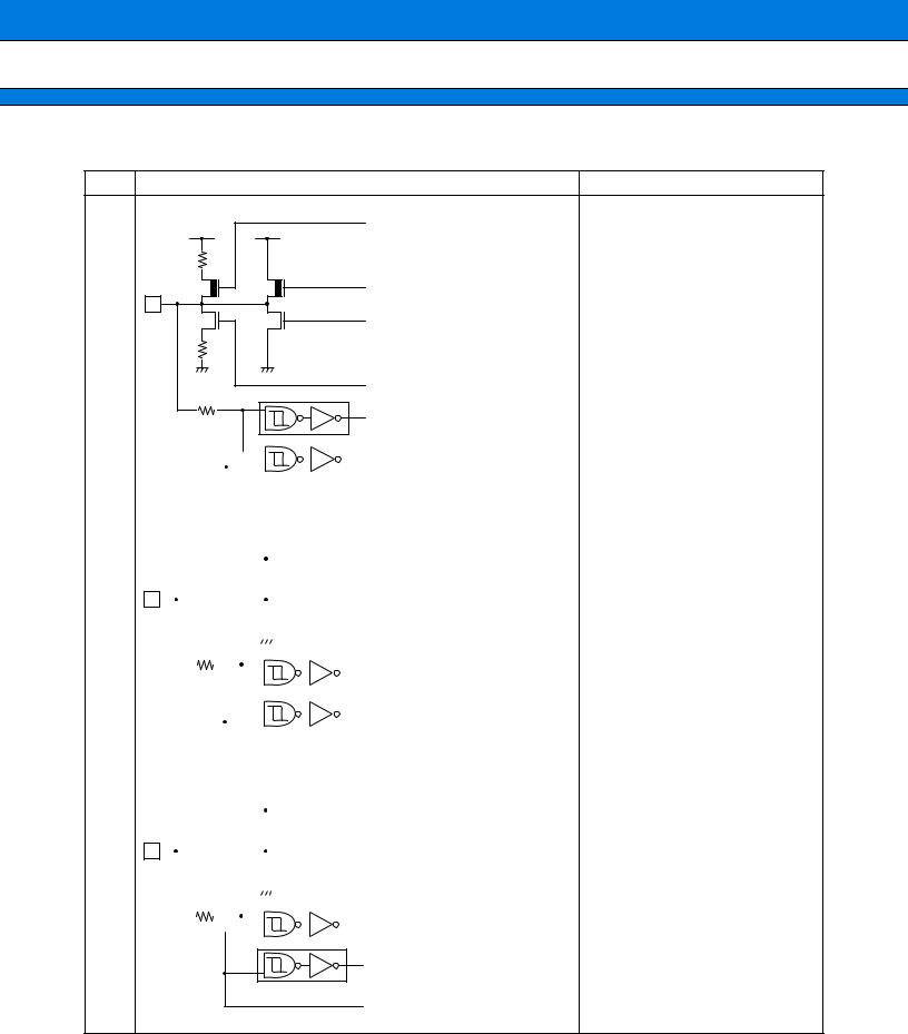
MB91270/280 Series
■ I/O CIRCUIT TYPE
Type |
Circuit |
Remarks |
|
|
Pull-up control |
• CMOS level output |
|
|
|
(IOL = 4 mA, IOH = −4 mA) |
||
|
|
|
||
|
|
|
• CMOS hysteresis input |
|
|
|
|
(With function to disconnect |
|
P-ch |
P-ch |
Pout |
input during standby mode. ) |
|
• Automotive input |
||||
|
|
|
||
N-ch |
N-ch |
Nout |
(With function to disconnect |
|
|
|
|
input during standby mode. ) |
|
A |
|
|
• Resistor that can be set |
|
|
|
Pull-down control |
pull-up resistor : Approx. 50 Ω |
|
|
|
|
||
|
|
CMOS hysteresis input |
|
|
|
|
|
|
|
|
|
|
|
|
|
|
|
|
|
|
|
|
Automotive input |
|
|
|
|
|
|
|
|
|
|
|
|
|
|
|
|
|
|
|
|
|
|
|
|
|
|
|
|
|
|
|
|
|
|
|
|
|
|
|
|
|
|
|
|
|
|
|
|
|
|
|
|
|
|
|
|
|
|
|
|
|
|
|
|
|
|
|
|
|
|
|
|
|
|
|
|
|
|
|
|
|
|
|
Standby control for |
|
|
|
|
|
|
|
|
|
|
|
|
|
|
|
|
|
|
|
|
|
|
|
|
|
|
|
|
|
|
|
|
|
|
|
|
|
|
|
|
|
|
|
|
|
|
|
|
|
|
|
|
|
|
|
|
|
|
|
|
|
|
disconnect input |
|
|
|
|
|
|
|
|
|
|
|
|
|
|
|
|
|
|
|
|
|
|
|
|
|
|
|
|
|
|
|
|
|
|
|
|
|
|
|
|
|
|
• CMOS level output |
|
|
|
|
|
|
|
|
|
|
|
|
|
|
|
|
|
|
|
|
(IOL = 4 mA, IOH = −4 mA) |
|
|
|
|
|
|
|
|
|
|
|
|
|
|
|
|
|
|
|
|
|
|
|
|
|
|
|
|
|
|
|
|
|
|
|
|
|
|
• CMOS hysteresis input |
|||
|
|
|
|
|
P-ch |
|
|
|
|
|
Pout |
|||||||||
|
|
|
|
|
|
|
|
|
|
|
|
|||||||||
|
|
|
|
|
|
|
|
|
|
|
|
|
|
|
|
|
|
|
Nout |
(With function to disconnect |
|
|
|
|
|
|
|
|
|
|
|
|
|
|
|
|
|
|
|
||
|
|
|
|
|
N-ch |
|
|
|
|
|
input during standby mode. ) |
|||||||||
|
|
|
|
|
|
|
|
|
|
|
|
|||||||||
B |
|
|
|
|
|
|
|
|
|
|
|
|
|
|
|
|
|
|
• Automotive input |
|
|
|
|
|
|
|
|
|
|
|
|
|
|
|
|
|
|
|
|||
|
|
|
|
|
|
|
|
|
|
|
|
|
|
CMOS hysteresis input |
(With function to disconnect |
|||||
|
|
|
|
|
|
|
|
|
|
|
|
|
|
|
|
|
||||
|
|
|
|
|
|
|
|
|
|
|
|
|
|
|
|
|
|
|
input during standby mode. ) |
|
|
|
|
|
|
|
|
|
|
|
|
|
|
|
|
|
|
|
|
||
|
|
|
|
|
|
|
|
|
|
|
|
|
|
|
|
|
|
|
Automotive input |
|
|
|
|
|
|
|
|
|
|
|
|
|
|
|
|
|
|
|
|
|
|
|
|
|
|
|
|
|
|
|
|
|
|
|
|
|
|
|
|
|
|
|
|
|
|
|
|
|
|
|
|
|
|
|
|
|
|
|
|
|
|
|
|
|
|
|
|
|
|
|
|
|
|
|
|
|
|
|
|
|
|
|
|
|
|
|
|
|
|
|
|
|
|
|
|
|
|
|
|
|
|
|
|
|
|
|
|
|
|
|
|
|
|
|
|
|
|
|
|
|
|
|
|
|
Standby control for |
|
|
|
|
|
|
|
|
|
|
|
|
|
|
|
|
|
|
|
|
|
|
|
|
|
|
|
|
|
|
|
|
|
|
|
|
|
|
|
|
|
disconnect input |
|
|
|
|
|
|
|
|
|
|
|
|
|
|
|
|
|
|
|
|
|
|
|
|
|
|
|
|
|
|
|
|
|
|
|
|
|
|
|
|
|
|
• CMOS level output |
|
|
|
|
|
|
|
|
|
|
|
|
|
|
|
|
|
|
|
|
(IOL = 3 mA, IOH = −3 mA) |
|
|
|
|
|
|
|
|
|
|
|
|
|
|
|
|
|
|
|
|
|
|
|
|
|
|
|
|
|
|
|
|
|
|
|
|
|
• CMOS hysteresis input |
||||
|
|
|
|
|
P-ch |
|
|
|
|
|
Pout |
|||||||||
|
|
|
|
|
|
|
|
|
|
|
|
|||||||||
|
|
|
|
|
|
|
|
|
|
|
|
|
|
|
|
|
|
|
Nout |
(With function to disconnect |
|
|
|
|
|
|
|
|
|
|
|
|
|
|
|
|
|
|
|
||
|
|
|
|
|
N-ch |
|
|
|
|
|
input during standby mode. ) |
|||||||||
|
|
|
|
|
|
|
|
|
|
|
|
|||||||||
C |
|
|
|
|
|
|
|
|
|
|
|
|
|
|
|
|
|
|
• Automotive input |
|
|
|
|
|
|
|
|
|
|
|
|
|
|
|
|
|
|
|
|||
|
|
|
|
|
|
|
|
|
CMOS hysteresis input |
(With function to disconnect |
||||||||||
|
|
|
|
|
|
|
|
|
|
|
|
|
|
|
|
|
||||
|
|
|
|
|
|
|
|
|
|
|
|
|
|
|
|
|
|
|
input during standby mode. ) |
|
|
|
|
|
|
|
|
|
|
|
|
|
|
|
|
|
|
|
|
||
|
|
|
|
|
|
|
|
|
|
|
|
|
|
|
|
|
|
|
|
|
|
|
|
|
|
|
|
|
|
|
|
|
|
|
|
|
|
|
|
|
|
|
|
|
|
|
|
|
|
|
|
|
|
|
|
|
|
|
|
|
|
|
Automotive input
Standby control for disconnect input
(Continued)
20
MB91270/280 Series
|
|
|
|
|
|
|
|
|
|
|
|
|
|
|
|
|
|
|
|
|
|
|
Type |
|
|
|
|
|
|
Circuit |
Remarks |
||||||||||||
|
|
|
|
|
|
|
|
|
|
|
|
|
|
|
|
|
|
|
|
|
|
|
|
|
|
|
|
|
|
|
|
|
|
|
|
|
|
|
|
|
|
• CMOS level output |
|
|
|
|
|
|
|
|
|
|
|
|
|
|
|
|
|
|
|
|
|
(IOL = 3 mA, IOH = −3 mA) |
|
|
|
|
|
|
|
|
|
|
|
|
|
|
|
|
|
|
|
|
|
||
|
|
|
|
|
|
|
|
|
|
|
|
|
|
|
|
|
|
Pout |
• CMOS hysteresis input |
||
|
|
|
|
|
|
P-ch |
|
|
|
|
|
|
|
|
|
||||||
|
|
|
|
|
|
|
|
|
|
|
|||||||||||
|
|
|
|
|
|
|
|
|
|
|
|
|
|
|
|
|
|
|
Nout |
(With function to disconnect |
|
|
|
|
|
|
|
|
|
|
|
|
|
|
|
|
|
|
|
|
|||
|
|
|
|
|
|
N-ch |
|
|
|
|
|
|
|
|
|
input during standby mode. ) |
|||||
|
|
|
|
|
|
|
|
|
|
|
|||||||||||
|
|
|
|
|
|
|
|
|
|
|
|
|
|
|
|
|
|
|
|
• Automotive input |
|
|
|
|
|
|
|
|
|
|
|
|
|
|
|
|
|
|
|
|
|
||
|
|
|
|
|
|
|
|
|
|
|
|
|
|
|
|
|
|
|
CMOS hysteresis input |
(With function to disconnect |
|
|
|
|
|
|
|
|
|
|
|
|
|
|
|
|
|
|
|
|
|||
|
CA |
|
|
|
|
|
|
|
|
|
|
|
|
|
input during standby mode. ) |
||||||
|
|
|
|
|
|
|
|
|
|
|
|
|
|
||||||||
|
|
|
|
|
|
|
|
|
|
|
|
|
|
||||||||
|
|
|
|
|
|
|
|
|
|
|
|
|
|
|
|||||||
|
|
|
|
|
|
|
|
|
|
|
|
|
|
|
|
|
|
|
Automotive input |
• A/D analog input |
|
|
|
|
|
|
|
|
|
|
|
|
|
|
|
|
|
|
|
|
|||
|
|
|
|
|
|
|
|
|
|
|
|
|
|
|
|
|
|
|
|
|
|
|
|
|
|
|
|
|
|
|
|
|
|
|
|
|
|
|
|
|
|
|
|
|
|
|
|
|
|
|
|
|
|
|
|
|
|
|
|
|
|
|
Standby control for |
|
|
|
|
|
|
|
|
|
|
|
|
|
|
|
|
|
|
|
|
|
|
|
|
|
|
|
|
|
|
|
|
|
|
|
|
|
|
|
|
|
|
|
disconnect input |
|
|
|
|
Analog input |
|
|
|
Pull-up control |
• CMOS level output |
|
|
(IOL = 4 mA, IOH = −4 mA) |
|
|
|
|
|
|
|
|
• CMOS hysteresis input |
|
|
|
(With function to disconnect |
P-ch |
P-ch |
Pout |
input during standby mode. ) |
|
|
|
• Automotive input |
N-ch |
N-ch |
Nout |
(With function to disconnect |
|
|
|
input during standby mode. ) |
|
|
|
• Resistor that can be set |
D |
|
Pull-down control |
pull-up resistor : Approx. 50 Ω |
|
• A/D analog input |
||
|
|
|
|
|
|
CMOS hysteresis input |
|
|
|
Automotive input |
|
|
|
Standby control for |
|
|
|
disconnect input |
|
|
|
Analog input |
|
|
|
|
(Continued) |
21

MB91270/280 Series
Type |
|
Circuit |
Remarks |
|
|
|
• CMOS level output |
|
P-ch |
Pout |
(IOL = 4 mA, IOH = −4 mA) |
|
• CMOS hysteresis input |
||
|
N-ch |
Nout |
(With function to disconnect |
|
input during standby mode. ) |
||
|
|
|
|
|
|
|
• Automotive input |
|
|
CMOS hysteresis input |
(With function to disconnect |
|
|
input during standby mode. ) |
|
|
|
|
|
E |
|
Automotive input |
• A/D analog input |
|
• D/A analog output |
||
|
|
||
|
|
|
|
|
|
Standby control for |
|
|
|
disconnect input |
|
|
|
Analog input |
|
|
|
Analog output |
|
|
|
|
CMOS hysteresis input |
J |
|
CMOS hysteresis input |
|
|
|
|
• CMOS hysteresis input |
|
|
|
• Pull-up resistor value : |
Pull-up resistor |
|
Approx. 50 kΩ |
|
N |
|
|
|
|
|
CMOS hysteresis input |
|
|
|
Pull-up control |
• CMOS level output |
|
|
(IOL = 4 mA, IOH = −4 mA) |
|
|
|
|
|
|
|
|
• CMOS hysteresis input |
|
|
|
(With function to disconnect |
P-ch |
P-ch |
Pout |
input during standby mode. ) |
|
|
|
• Automotive input |
N-ch |
N-ch |
Nout |
(With function to disconnect |
|
|
|
input during standby mode. ) |
|
|
|
• TTL |
T |
|
Pull-down control |
(With function to disconnect |
|
|
input during standby mode. ) |
|
|
|
|
|
|
|
CMOS hysteresis input |
• Resistor that can be set |
|
|
|
pull-up resistor : Approx. 50 kΩ |
|
|
Automotive input |
|
TTL input
Standby control for disconnect input
(Continued)
22
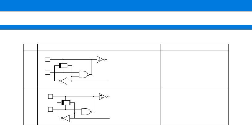
MB91270/280 Series
(Continued) |
|
|
|
Type |
|
Circuit |
Remarks |
|
|
|
Oscillation circuit |
|
X1 |
Xout |
High speed oscillation feed- |
OA |
|
|
back resistance = |
|
|
Approx. 1 MΩ |
|
OB |
X0 |
|
|
|
|
||
|
|
Standby control signal |
|
|
|
Oscillation circuit |
X1A |
Xout |
Low speed oscillation feed- |
WA |
|
back |
|
resistance = Approx. 10 MΩ |
|
WB X0A |
|
|
|
|
|
|
Standby control signal |
|
23

MB91270/280 Series
■ I/O CELL LIST
|
|
Input |
|
|
|
|
|
|
|
|
|
|
Output Driv- |
|
|
Type |
Pull Up/Down |
CMOS (C) |
Input Stop |
Analog Line |
Remarks |
||
|
CMOS Schmitt (CS) |
|
er |
|
|||
|
(50 kΩ) |
Automotive (A) |
|
|
|
|
|
|
|
|
|
|
|
||
|
|
|
|
|
|
|
|
A |
Up/Down switch |
CS/A switch |
Stop |
|
4 mA |
|
|
|
|
|
|
|
|
|
|
B |
|
CS/A switch |
Stop |
|
4 mA |
|
|
|
|
|
|
|
|
|
|
C* |
|
CS/A switch |
Stop |
|
3 mA |
I2C |
|
CA* |
|
CS/A switch |
Stop |
Input |
3 mA |
I2C + ADC |
|
D |
Up/Down switch |
CS/A switch |
Stop |
Input |
4 mA |
ADC |
|
|
|
|
|
|
|
|
|
E |
|
CS/A switch |
Stop |
I/O |
4 mA |
ADC + DAC |
|
|
|
|
|
|
|
|
|
J |
|
C |
|
|
|
MD[2 : 0] |
|
|
|
|
|
|
|
|
|
N |
Up |
CS (initx) |
|
|
|
INITX |
|
|
|
|
|
|
|
|
|
T |
Up/Down switch |
CS/A/TTL switch |
Stop |
|
4 mA |
Has TTL |
|
input |
|||||||
|
|
|
|
|
|
||
|
|
|
|
|
|
|
|
OA |
|
|
Stop |
|
|
4 MHz |
|
OB |
Oscillator |
||||||
|
|
|
|
|
|||
|
|
|
|
|
|
|
|
WA |
|
|
Stop |
|
|
32 kHz |
|
WB |
Oscillator |
||||||
|
|
|
|
|
|||
|
|
|
|
|
|
|
* : When the C and CA ports are set for use as an I2C interface, the outputs are Nch open drain outputs. Otherwise, functions as a CMOS output.
■ PIN INPUT VOLTAGE
Form |
Type |
VIL |
VIH |
|
|
|
|
C |
CMOS input |
VSS + 0.3 V |
VCC − 0.3 V |
|
|
|
|
CS (initx) |
CMOS Schmitt trigger input (for INITX pin) |
0.2 VCC |
0.8 VCC |
|
|
|
|
CS |
CMOS Schmitt trigger input |
0.3 VCC |
0.7 VCC |
|
|
|
|
A |
CMOS automotive Schmitt trigger input |
0.5 VCC |
0.8 VCC |
|
|
|
|
T |
TTL input |
0.8 V |
2.1 V |
|
|
|
|
24
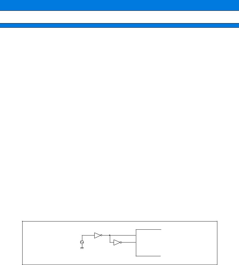
MB91270/280 Series
■ HANDLING DEVICES
• Preventing Latch-up
Latch-up may occur in a CMOS IC if a voltage greater than VCC or less than VSS is applied to an input or output pin or if an above-rating voltage is applied between VCC pin and VSS pin. A latch-up, if it occurs, significantly increases the power supply current and may cause thermal destruction of an element. When you use a CMOS IC, do not exceed the maximum rating.
• Treatment of Unused Pins
Do not leave an unused input pin open, since it may cause a malfunction. Handle by, for example, using a pullup or pull-down resistor.
• About Power Supply Pins
In products with multiple VCC or VSS pins, the pins of the same potential are internally connected in the device to avoid abnormal operations including latch-up. However, you must connect the pins to external power supply and a ground line to lower the electro-magnetic emission level, to prevent abnormal operation of strobe signals caused by the rise in the ground level, and to conform to the total output current rating.
Moreover, connect the current supply source with the VCC and VSS pins of this device at the low impedance.
It is also advisable to connect a ceramic bypass capacitor of approximately 0.1 F between VCC and VSS near this device.
• About Crystal Oscillator Circuit
Noise near the X0, X1, X0A and X1A pins may cause the device to malfunction. Design the printed circuit board so that X0, X1, X0A and X1A the crystal oscillator (or ceramic oscillator), and the bypass capacitor to ground are located as close to the device as possible.
It is strongly recommended to design the PC board artwork with the X0, X1, X0A and X1A pins surrounded by ground plane because stable operation can be expected with such a layout.
Please ask the crystal maker to evaluate the oscillational characteristics of the crystal and this device.
• Notes on Using External Clock
When external clock is selected, supply it to X0 pin generally, and simultaneously the opposite phase clock to X0 must be supplied to X1 pin. However, in this case the stop mode (oscillation stop mode) must not be used. (This is because the X1 pin stops at High level output in STOP mode.)
Using an external clock (normal)
X0
X1
Note : The STOP mode (oscillation stop mode) cannot be used.
• Notes when using no sub-clock
Use a single-clock model if not using the sub-clock.
25

MB91270/280 Series
Always connect a resonator of 100 kHz or less on dual clock models.
• Treatment of N.C. or OPEN pins
Pins marked as N.C. and OPEN must be left open - circuit.
• About Mode pins (MD0 to MD2)
These pins should be connected directly to VCC or VSS. To prevent the device erroneously switching to test mode due to noise, design the printed circuit board such that the distance between the mode pins and VCC or VSS is as short as possible and the connection impedance is low.
• Operation at start-up
The INITX pin must be held at the “L”level when turning on the power.
• Source oscillation input at power on
When turning the power on, maintain clock input until the device is released from the oscillation stabilization wait state.
• Caution on Operations during PLL Clock Mode
Even if the oscillator comes off or the clock input stops with the PLL clock selected for this microcontroller, the microcontroller may continue to operate at the free-running frequency of the PLL’s internal self-oscillating oscillator circuit.
Performance of this operation, however, cannot be guaranteed.
• External bus setting
This device is guaranteed for use with a 16 MHz external bus.
If the base clock is set to 32 MHz with DIVR1 (external bus base clock division setting register) set to its initial value, the external bus also operates at 32 MHz. When changing the base clock, first set the external bus so that it will not exceed 16 MHz.
• Pull-up control
The AC characteristics cannot be guaranteed if pull-up resistors are used for pins used as external bus pins.
26
Loading...