


MB89643
FUJITSU MB89643, MB89645, MB89646, MB89647, MB89P647 DATA SHEET
...
DS07-12505-3E
FUJITSU SEMICONDUCTOR
DATA SHEET
8-bit Proprietary Microcontroller
CMOS
F
2
MC-8L MB89640 Series
MB89643/645/646/647/P647/PV640
■
DESCRIPTION
The MB89640 series has been developed as a general-purpose version of the F
2
MC*-8L family consisting of
proprietary 8-bit, single-chip microcontrollers.
In addition to a compact instruction set, the microcontrollers contain a variety of peripheral functions such as
dual-clock control system, five operating speed control stages, timers, a PWM timer, serial interface, an A/D
converter, a D/A converter, an external interrupt, and a watch prescaler.
*: F
2
MC stands for FUJITSU Flexible Microcontroller.
■
FEATURES
•F
2
MC-8L family CPU core
Instruction set optimized for controllers
(Continued)
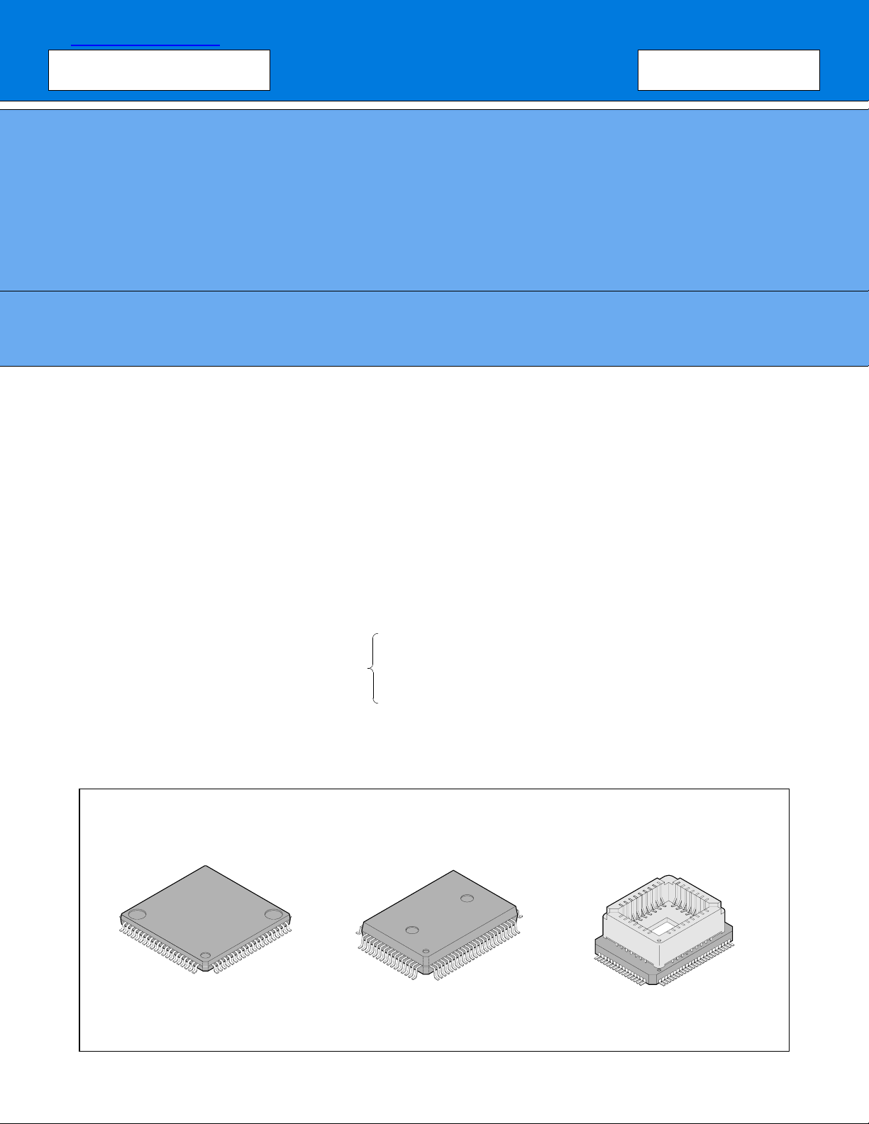
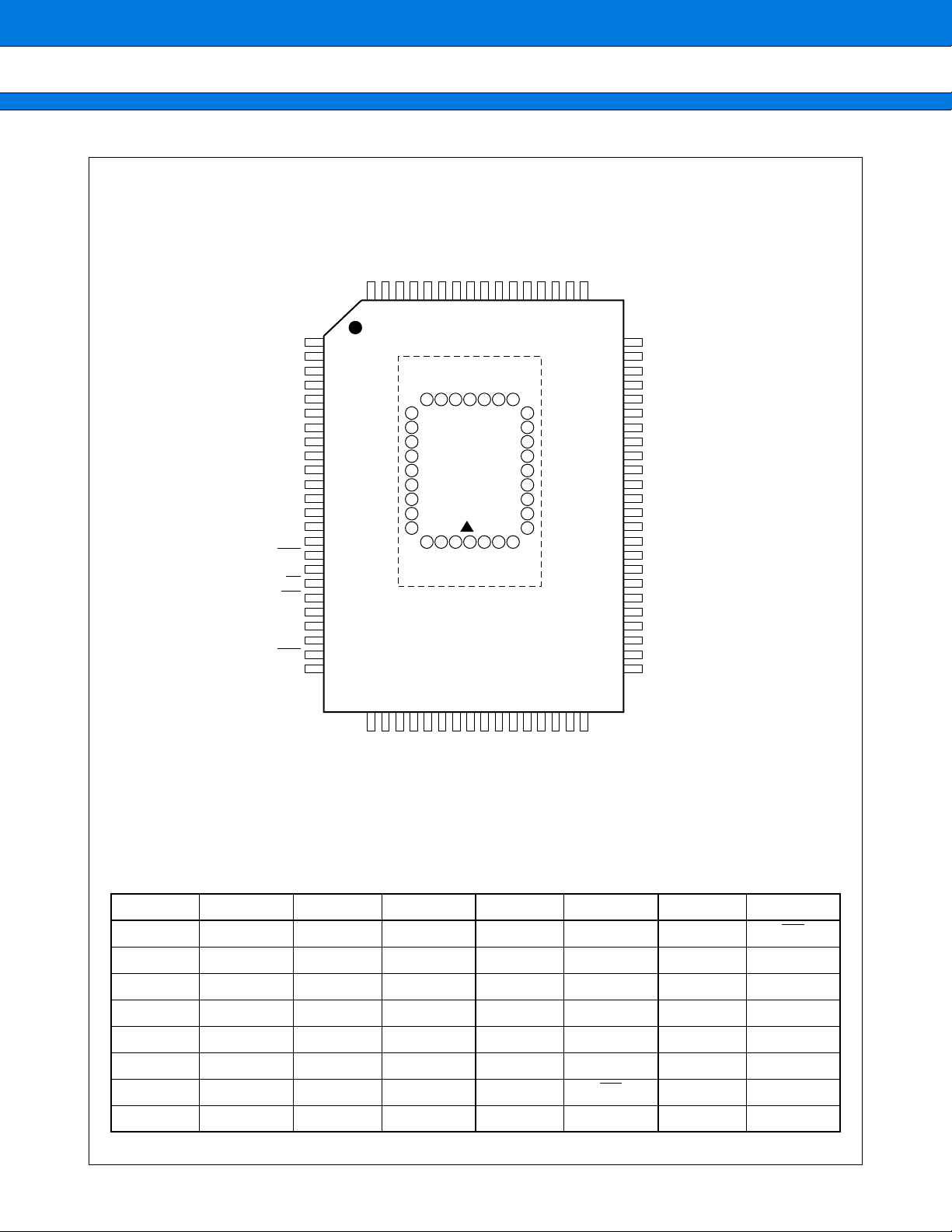
■
PACKAGE
Multiplication and division instructions
16-bit arithmetic operations
Test and branch instructions
Bit manipulation instructions, etc.
(FPT-80P-M11) (FPT-80P-M06) (MQP-80C-P01)
80-pin Plastic QFP
80-pin Plastic QFP
80-pin Ceramic MQFP
查询MB89643供应商

2
MB89640 Series
(Continued)
• Six types of timers
8-bit PWM timer: 2 channels (also usable reload timer)
8-bit pulse width counter (continuous measurement capable and applicable to remote control)
16-bit timer/counter
21-bit time-base counter
15-bit watch prescaler
• Two 8-bit serial I/O
Swichable transfer direction allows communication with various equipment.
• 8-bit A/D converter: 8 channels
Sense mode function enabling comparison at 12 instructions
Activation by external input capable
• External interrupt 1, external interrupt 2: 9 channels
• 8-bit D/A converter: 2 channels
8-bit R-2R type
• Low-power consumption modes (stop mode, sleep mode, watch mode, subclock mode)
• Bus interface functions
Including hold and ready functions
3
MB89640 Series
■
PRODUCT LINEUP
(Continued)
MB89643 MB89645 MB89646 MB89647 MB89P647 MB89PV640
Classification
Mass production products
(mask ROM products)
One-time
PROM product
Piggyback/
evaluation product
for evaluation and
development
ROM size 8 K × 8 bits
(internal mask
ROM)
16 K × 8 bits
(internal mask
ROM)
24 K × 8 bits
(internal mask
ROM)
32 K × 8 bits
(internal mask
ROM)
32 K × 8 bits
(internal PROM,
programming with
general-purpose
programmer)
32 K × 8 bits
(external ROM)
RAM size 256 × 8 bits 512 × 8 bits 768 × 8 bits 1 K × 8 bits
CPU functions Number of instructions: 136
Instruction bit length: 8 bits
Instruction length: 1 to 3 bytes
Data bit length: 1, 8, 16 bits
Minimum execution time: 0.4 µs/10 MHz to 6.4 µs/10 MHz,
or 61.0 µs/32.768 kHz
Interrupt processing time: 3.6 µs/10 MHz to 57.6 µs/10 MHz,
or 562.5 µs/32.768 kHz
Ports Input ports (CMOS): 9 (All also serve as a external interrupt.)
Output ports (CMOS): 8 (All also serve as a bus control.)
I/O ports (CMOS): 24 (8 ports also serve as peripherals,
16 ports also serve as a bus control.)
I/O ports (N-ch open-drain): 8 (All also serve as peripherals.)
Output ports (N-ch open-drain): 16 (8 ports also serve as peripherals.)
Total: 65
Clock timer 21 bits × 1 (in main clock mode), 15 bits × 1 (at 32.768 kHz)
8-bit PWM
timer
8-bit reload timer operation × 2 channels
7/8-bit resolution PWM operation × 2 channels
8-bit PPG operation × 1 channel
8-bit pulse
width counter
8-bit timer operation (overflow output capable)
8-bit reload timer operation (toggled output capable)
8-bit pulse width measurement operation
(Continuous measurement capable, measurement of “H” width/“L” width/from ↑ to ↓/from ↓ to ↑ capable)
16-bit timer/
counter
16-bit timer operation
16-bit event counter operation
8-bit serial I/O 8 bits × 2 channels
LSB first/MSB first selectability
One clock selectable from four transfer clocks
(one external shift clock, three internal shift clocks: 0.8 µs, 3.2 µs, 12.8 µs)
8-bit A/D
converter
8-bit resolution × 8 channels
A/D conversion mode (conversion time: 44 instructions)
Sense mode (conversion time: 12 instructions)
Continuous activation by an external activation or an internal timer capable
Reference voltage input
Part number
Parameter
4
MB89640 Series
(Continued)
*1: Varies with conditions such as the operating frequency. (See section “■ Electrical Characteristics.”)
■
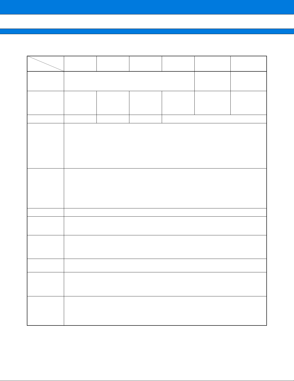
PACKAGE AND CORRESPONDING PRODUCTS
: Available
× : Not available
Note: For more information about each package, see section “■ External Dimensions.”
MB89643 MB89645 MB89646 MB89647 MB89P647 MB89PV640
8-bit D/A
converter
8-bit resolution × 2 channels, R-2R type
External interrupt 1,
External interrupt 2
9 channels
Standby modes Watch mode, subclock mode, sleep mode, and stop mode
Process CMOS
Operating
voltage*
1
2.2 V to 6.0 V 2.7 V to 6.0 V
EPROM for use
MBM27C256A
-20TV
Package
MB89643
MB89645
MB89646
MB89647
MB89P647
MB89PV640
FPT-80P-M11 ×
FPT-80P-M06 ×
MQP-80C-P01 ×
Part number
Parameter

5
MB89640 Series
■
DIFFERENCES AMONG PRODUCTS
1. Memory Size
Before e v aluating using the piggyback product, v erify its diff erences from the product that will actually be used.
Take particular care on the following points:
• On the MB89643 register banks 16 to 32 cannot be used.
• On the MB89P647, the program area starts from address 8007
H but on the MB89PV640 and MB89647 starts
from 8000H.
(On the MB89P647, addresses 8000
H to 8006H comprise the option setting area, option settings can be read
by reading these addresses. On the MB89PV640 and MB89647, addresses 8000
H to 8006H could also be
used as a program ROM. However, do not use these addresses in order to maintain compatibility of the
MB89P647.)
• The stack area, etc., is set at the upper limit of the RAM.
• The external areas are used.
2. Current Consumption
• In the case of the MB89PV640, add the current consumed by the EPROM which is connected to the top soc ket.
• When operated at low speed, the product with an OTPROM (one-time PROM) or an EPROM will consume
more current than the product with a mask ROM.
• However, the current consumption in sleep/stop modes is the same. (For more information, see sections
“■ Electrical Characteristics” and “■ Example Characteristics.”)
3. Mask Options
Functions that can be selected as options and how to designate these options vary by the product.
Before using options check section “■ Mask Options.”
Take particular care on the following points:
• A pull-up resistor cannot be set for P40 to P47 and P50 to P57 on the MB89P647.
• For all products, P60 to P67 are available for no pull-up resistor when an A/D converter is used.
• For all products, P50 to P57 are available for no pull-up resistor when a D/A converter is used.
• Options are fixed on the MB89PV640.
6
MB89640 Series
■
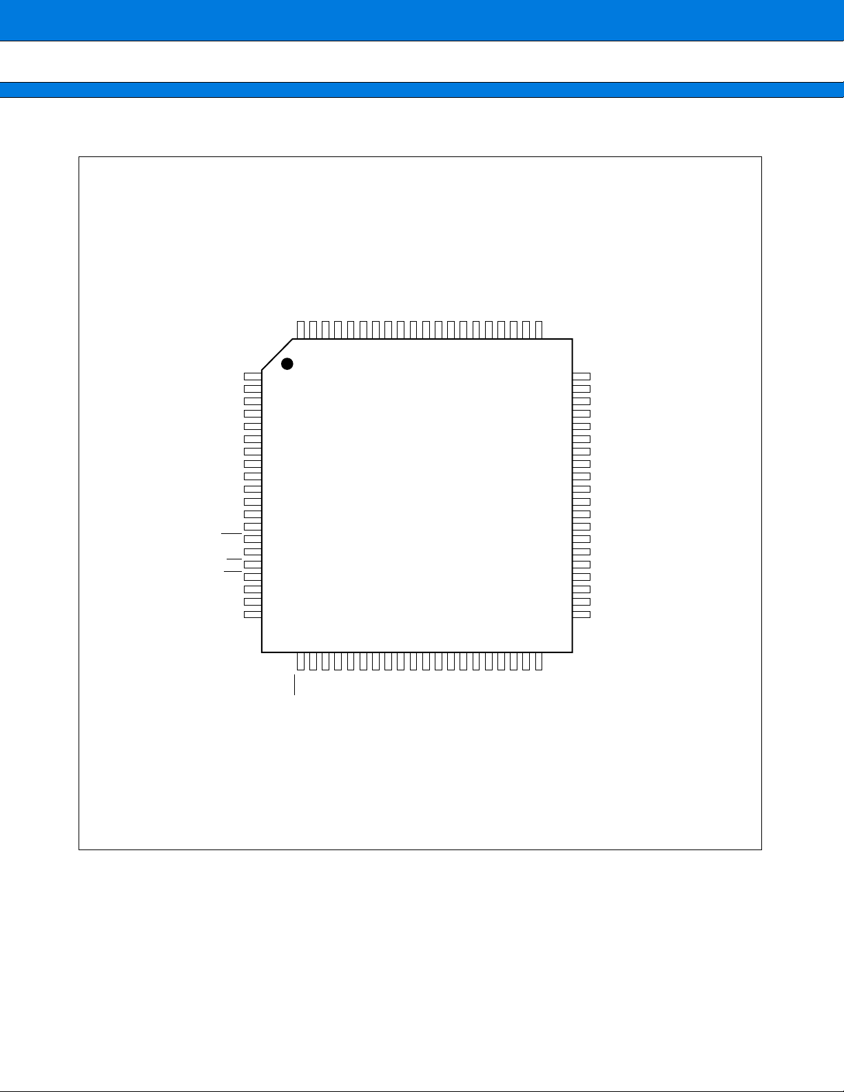
PIN ASSIGNMENT
1
2
3
4
5
6
7
8
9
10
11
12
13
14
15
16
17
18
19
20
P71/LI1
P70/LI0
P83/INT3
P82/INT2
P81/INT1
P80/INT0
X0A
X1A
MOD0
MOD1
X0
X1
V
SS
RST
P27/ALE
P26/RD
P25/WR
P24/CLK
P23/RDY
P22/HRQ
60
59
58
57
56
55
54
53
52
51
50
49
48
47
46
45
44
43
42
41
P54/BZ
P55/SCK2
P56/SO2
P57/SI2
V
SS
P40
P41
V
CC
P42
P43
P44
P45
P46
P47
P30/ADST
P31/SCK1
P32/SO1
P33/SI1
P34/EC
P35/PWC
80
79
78
77
76
75
74
73
72
71
70
69
68
67
66
65
64
63
62
61
P72/LI2
P73/LI3
P74/LI4
P60/AN0
P61/AN1
P62/AN2
P63/AN3
P64/AN4
P65/AN5
P66/AN6
P67/AN7
AV
SS
AVRL
AVRH
AV
CC
DAVC
P50/DA1
P51/DA2
P52/PWM
P53/PTO2
21
22
23
24
25
26
27
28
29
30
31
32
33
34
35
36
37
38
39
40
P21/HAK
P20/BUFC
P17/A15
P16/A14
P15/A13
P14/A12
P13/A11
P12/A10
P11/A09
P10/A08
P07/AD7
P06/AD6
P05/AD5
P04/AD4
P03/AD3
P02/AD2
P01/AD1
P00/AD0
P37/PTO1
P36/WTO
(FPT-80P-M11)
(Top view)
7
MB89640 Series
• Pin assignment on package top (MB89PV640 only)
N.C.: Internally connected. Do not use.
Pin no. Pin name Pin no. Pin name Pin no. Pin name Pin no. Pin name
81 N.C. 89 A2 97 N.C. 105 OE
82 VPP 90 A1 98 O4 106 N.C.
83A1291A099O5107A11
84 A7 92 N.C. 100 O6 108 A9
85 A6 93 O1 101 O7 109 A8
86 A5 94 O2 102 O8 110 A13
87 A4 95 O3 103 CE
111 A14
88 A3 96 V
SS 104 A10 112 VCC
1
2
3
4
5
6
7
8
9
10
11
12
13
14
15
16
17
18
19
20
21
22
23
24
P73/LI3
P72/LI2
P71/LI1
P70/LI0
P83/INT3
P82/INT2
P81/INT1
P80/INT0
X0A
X1A
MOD0
MOD1
X0
X1
V
SS
RST
P27/ALE
P26/RD
P25/WR
P24/CLK
P23/RDY
P22/HRQ
P21/HAK
P20/BUFC
64
63
62
61
60
59
58
57
56
55
54
53
52
51
50
49
48
47
46
45
44
43
42
41
P52/PWM
P53/PTO2
P54/BZ
P55/SCK2
P56/SO2
P57/SI2
V
SS
P40
P41
V
CC
P42
P43
P44
P45
P46
P47
P30/ADST
P31/SCK1
P32/SO1
P33/SI1
P34/EC
P35/PWC
P36/WTO
P37/PTO1
80
79
78
77
76
75
74
73
72
71
70
69
68
67
66
65
P74/LI4
P60/AN0
P61/AN1
P62/AN2
P63/AN3
P64/AN4
P65/AN5
P66/AN6
P67/AN7
AV
SS
AVRL
AVRH
AV
CC
DAVC
P50/DA1
P51/DA2
25
26
27
28
29
30
31
32
33
34
35
36
37
38
39
40
P17/A15
P16/A14
P15/A13
P14/A12
P13/A11
P12/A10
P11/A09
P10/A08
P07/AD7
P06/AD6
P05/AD5
P04/AD4
P03/AD3
P02/AD2
P01/AD1
P00/AD0
101
102
103
104
105
106
107
108
109
93
92
91
90
89
88
87
86
85
100
99
98
97
96
95
94
110
111
112
81
82
83
84
(Top view)
(FPT-80P-M06)
(MQP-80C-P01)
Each pin inside the dashed line is for the
MB89PV640 only.
8
MB89640 Series
■
PIN DESCRIPTION
(Continued)
*1: FPT-80P-M11
*2: FPT-80P-M06
*3: MQP-80C-P01
Pin no.
Pin name
Circuit
type
Function
QFP
*1
QFP
*2
MQFP
*3
11 13 X0 A Main clock crystal oscillator pins (Max. 10 MHz)
12 14 X1
9 11 MOD0 C Operating mode selection pins
Connect directly to V
CC or VSS.
10 12 MOD1
14 16 RST D Reset I/O pin
This pin is an N-ch open-drain output type with pull-up
resistor, and a h ysteresis input type . “L” is output from this
pin by an internal reset source. The internal circuit is
initialized by the input of “L”.
38 to 31 40 to 33 P00/AD0 to
P07/AD7
E General-purpose I/O ports
Also serve as multiplex pins of lower address output and
data I/O.
30 to 23 32 to 25 P10/A08 to
P17/A15
E General-purpose I/O ports
Also serve as an upper address output.
22,
21,
18,
15
24,
23,
20,
17
P20/BUFC,
P21/HAK
,
P24/CLK,
P27/ALE
G General-purpose output-only ports
Also serve as a bus control signal output.
20,
19
22,
21
P22/HRQ,
P23/RDY
E General-purpose output-only ports
Also serve as a bus control signal input.
17,
16
19,
18
P25/WR
,
P26/RD
E General-purpose output-only ports
Also serve as a bus control signal output.
46 48 P30/ADST F General-purpose I/O port
Also serves as an A/D converter external activation. This
port is a hysteresis input type.
45 47 P31/SCK1 F General-purpose I/O port
Also serves as the clock I/O for the serial I/O 1. This port
is a hysteresis input type.
44,
43
46,
45
P32/SO1,
P33/SI1
F General-purpose I/O ports
Also serve as the data output for the serial I/O 1. These
ports are a hysteresis input type.
42 44 P34/EC F General-purpose I/O port
Also serves as the external clock input for the 16-bit timer/
counter. This port is a hysteresis input type.
9
MB89640 Series
(Continued)
*1: FPT-80P-M11
*2: FPT-80P-M06
*3: MQP-80C-P01
Pin no.
Pin name
Circuit
type
Function
QFP
*1
QFP
*2
MQFP
*3
41 43 P35/PWC F General-purpose I/O port
Also serves as the measured pulse input for the 8-bit pulse
width counter. This port is a hysteresis input type.
40 42 P36/WTO F General-purpose I/O port
Also serves as the toggle output for the 8-bit pulse width
counter. This port is a hysteresis input type.
39 41 P37/PTO1 F General-purpose I/O port
Also serves as the toggle output for the 1-channel PWM
timer.
55, 54,
52 to 47
57, 56,
54 to 49
P40 to P47 L N-ch medium-voltage open-drain output-only ports
64 66 P50/DA1 K N-ch open-drain I/O port
Also serves as a D/A channel 1 output. This port is a
hysteresis input type.
63 65 P51/DA2 K N-ch open-drain I/O port
Also serves as a D/A channel 2 output. This port is a
hysteresis input type.
62 64 P52/PWM H N-ch open-drain I/O port
Also serves as the PWM output by the two PWM timers.
This port is a hysteresis input type.
61 63 P53/PTO2 H N-ch open-drain I/O port
Also serves as the toggle output for the 2-channel PWM
timer. This port is a hysteresis input type.
60 62 P54/BZ H N-ch open-drain I/O port
Also serves as a buzzer output. This port is a hysteresis
input type.
59 61 P55/SCK2 H N-ch open-drain I/O port
Also serves as the clock I/O for the serial I/O 2. This port
is a hysteresis input type.
58 60 P56/SO2 H N-ch open-drain I/O port
Also serves as the data output for the serial I/O 2. This
port is a hysteresis input type.
57 59 P57/SI2 H N-ch open-drain I/O port
Also serves as the data input for the serial I/O 2. This port
is a hysteresis input type.
77 to 70 79 to 72 P60/AN0 to
P67/AN7
I N-ch open-drain output-only ports
Also serve as the analog input for the A/D converter.
These ports are a hysteresis input type.
2, 1,
80 to 78
4 to 1, 80 P70/LI0 to
P74/LI4
J Input-only ports
Also serve as external interrupt 1 input. These ports are a
hysteresis input type.
10
MB89640 Series
(Continued)
*1: FPT-80P-M11
*2: FPT-80P-M06
*3: MQP-80C-P01
Pin no.
Pin name
Circuit
type
Function
QFP
*1
QFP
*2
MQFP
*3
7 9 X0A B Subclock oscillator pins (32.768 kHz)
810X1A
53 55 V
CC Power supply pin
13, 56 15, 58 V
SS Power supply (GND) pin
66 68 AV
CC A/D converter power supply pin
Use this pin at the same voltage as VCC.
67, 68 69, 70 AVRH, AVRL A/D converter reference voltage input pins
65 67 DAVC D/A converter power supply pin
Use this pin at the same voltage as V
CC.
69 71 AVSS Analog circuit power supply pin
Use this pin at the same voltage as V
SS.
3 to 6 5 to 8 P83/INT3 to
P80/INT0
J Input-only ports
Also serve as an external interrupt 2 input. These ports
are a hysteresis input type.
11
MB89640 Series
• External EPROM pins (MB89PV640 only)
Pin no. Pin name I/O Function
82 V
PP O “H” level output pin
83
84
85
86
87
88
89
90
91
A12
A7
A6
A5
A4
A3
A2
A1
A0
O Address output pins
93
94
95
O1
O2
O3
I Data input pins
96 V
SS O Power supply (GND) pin
98
99
100
101
102
O4
O5
O6
O7
O8
I Data input pins
103 CE
O ROM chip enable pin
Outputs “H” during standby.
104 A10 O Address output pin
105 OE
O ROM output enable pin
Outputs “L” at all times.
107
108
109
A11
A9
A8
O Address output pins
110 A13 O
111 A14 O
112 V
CC O EPROM power supply pin
81
92
97
106
N.C. — Internally connected pins
Be sure to leave them open.
12
MB89640 Series
■
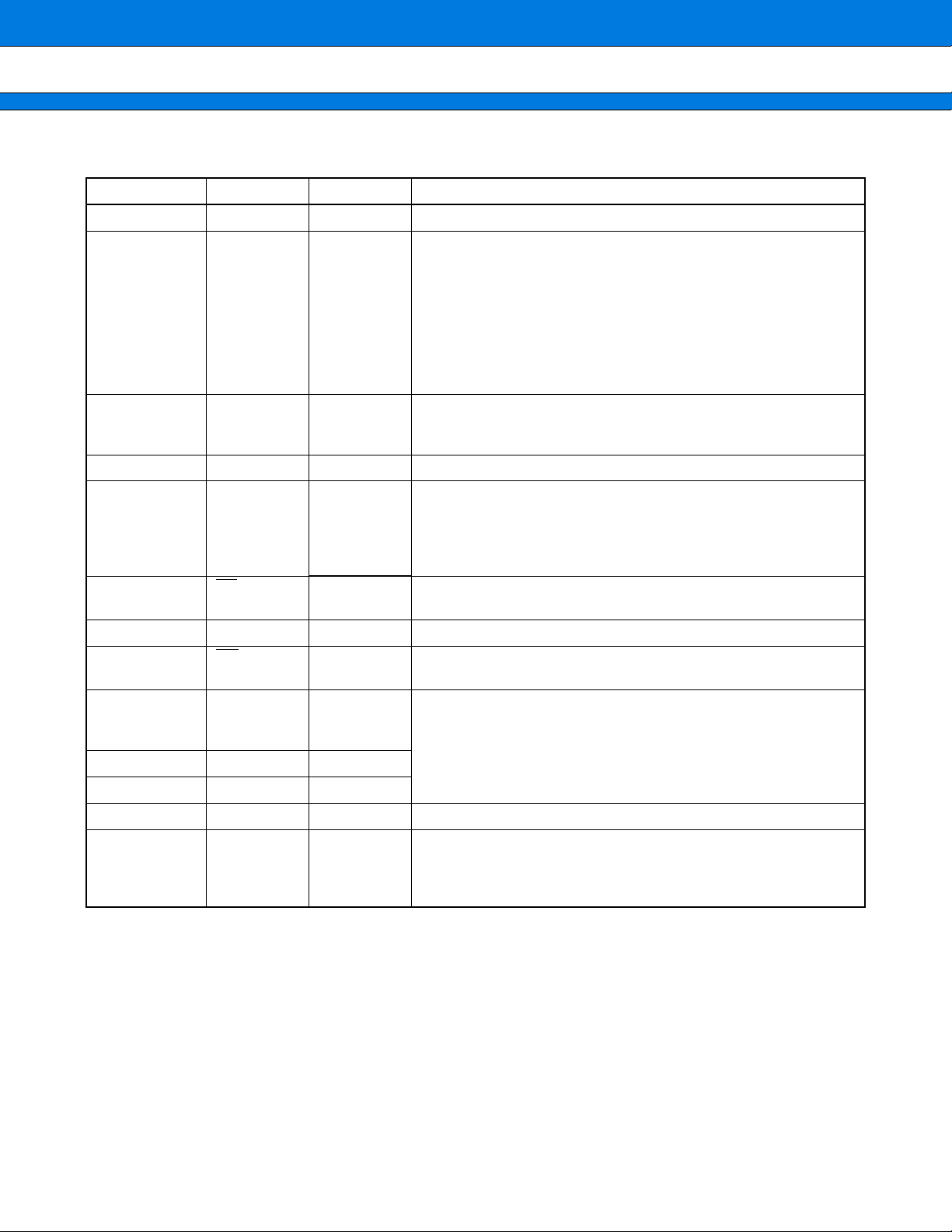
I/O CIRCUIT TYPE
(Continued)
Type Circuit Remarks
A Main clock
• At an oscillation feedback resistor of approximately
1 MΩ/5.0 V
B Subclock
• At an oscillation feedback resistor of approximately
4.5 MΩ/5.0 V
C
D • At an output pull-up resistor (P-ch) of approximately
50 kΩ/5.0 V
• Hysteresis input
E • CMOS output
• CMOS input
• Pull-up resistor optional
X1
X0
Standby control signal
X1A
X0A
Standby control signal
R
P-ch
N-ch
P-ch
N-ch
R
P-ch
13
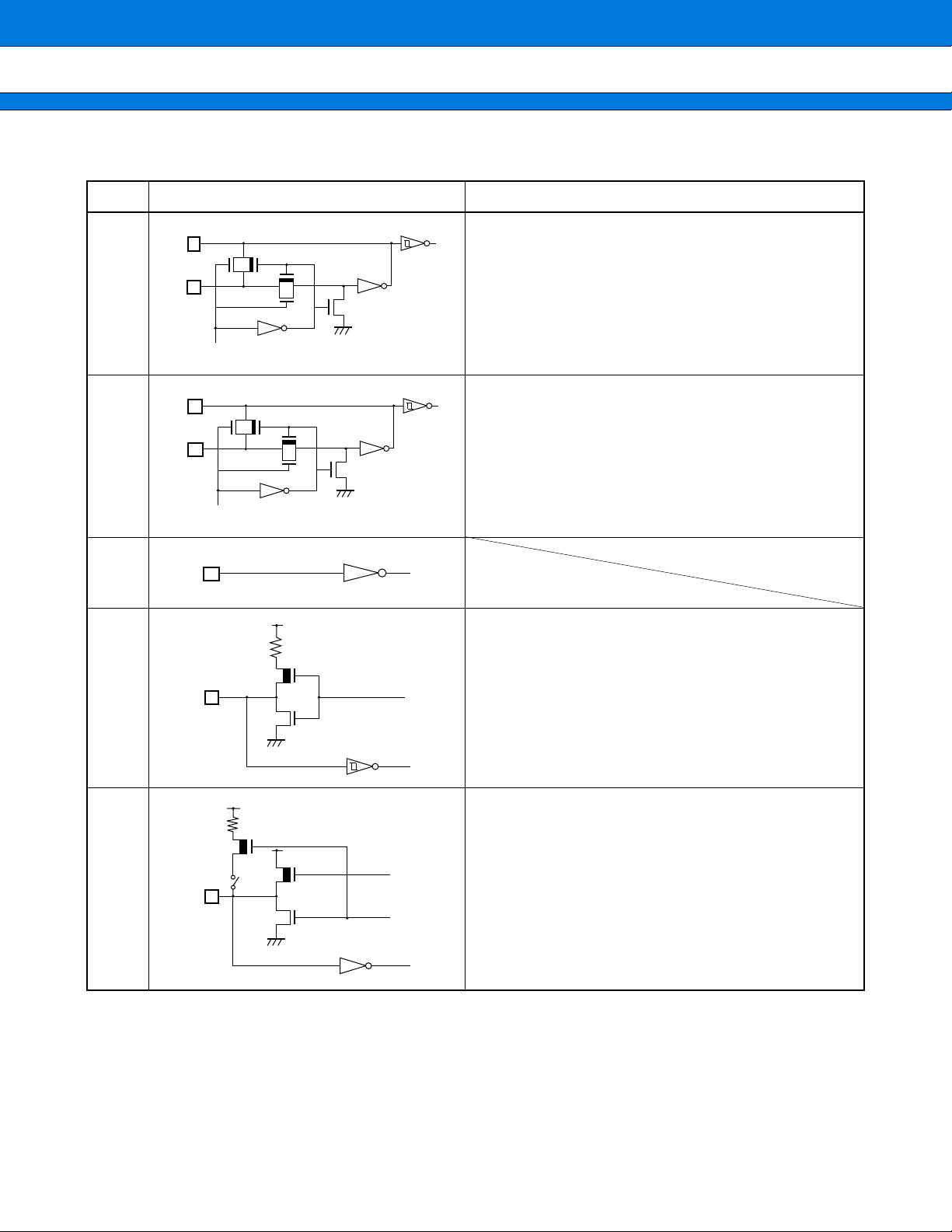
MB89640 Series
(Continued)
(Continued)
Type Circuit Remarks
F • CMOS output
• Hysteresis input
• Pull-up resistor optional
G • CMOS output
• Pull-up resistor optional
H • N-ch open-drain output
• Hysteresis input
• Pull-up resistor optional
I • N-ch open-drain output
• Analog input
• Pull-up resistor optional
J • Hysteresis input
• Pull-up resistor optional
P-ch
N-ch
P-ch
R
P-ch
N-ch
R
P-ch
N-ch
P-ch
R
N-ch
P-ch
Analog input
P-ch
R
R
14
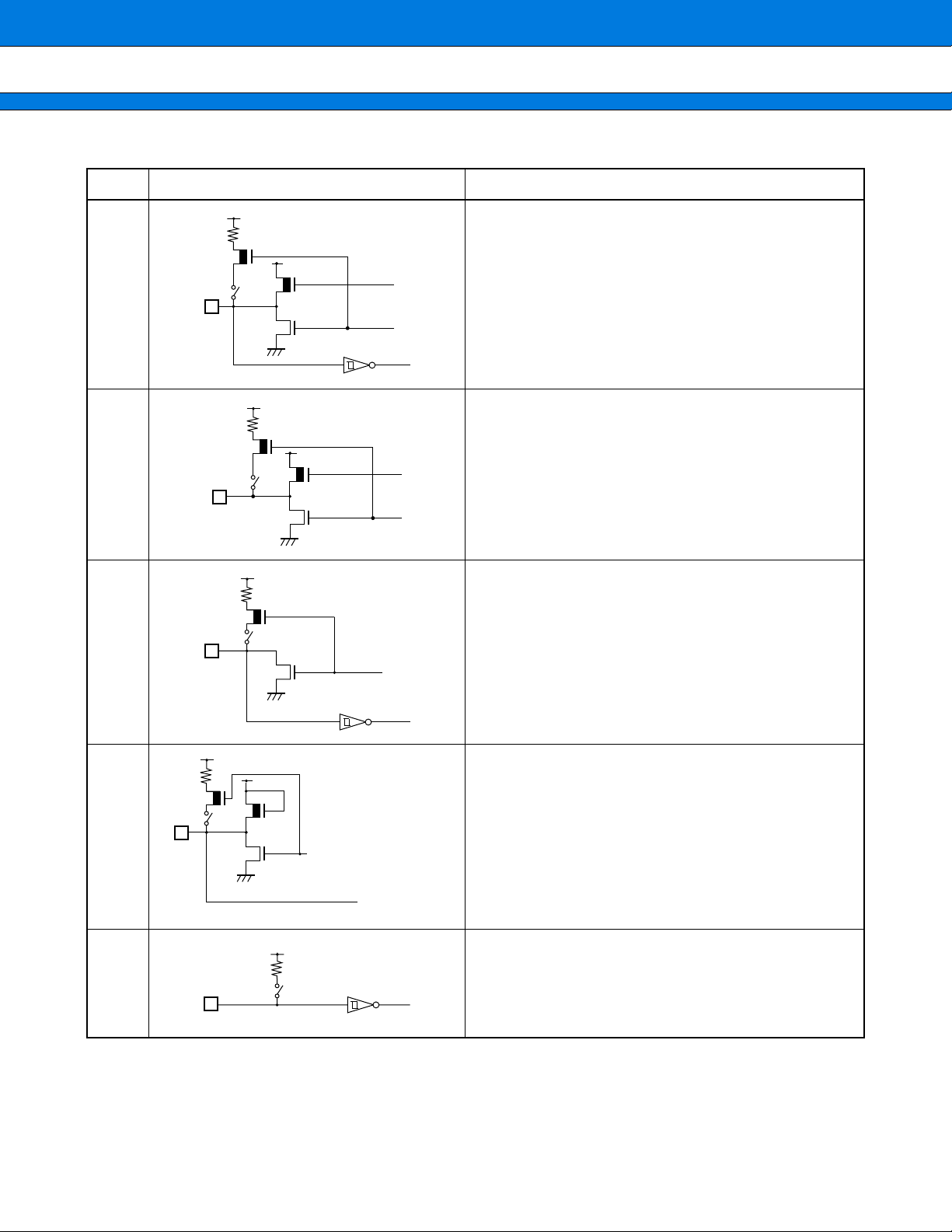
MB89640 Series
(Continued)
Type Circuit Remarks
K • N-ch open-drain output
• Hysteresis input
• Analog output
• Pull-up resistor optional
L • N-ch open-drain output
• Medium voltage
• Pull-up resistor optional
Enable
Analog output
N-ch
P-ch
P-ch
R
N-ch
P-ch
R

15
MB89640 Series
■
HANDLING DEVICES
1. Preventing Latchup
Latchup may occur on CMOS ICs if voltage higher than VCC or lo wer than VSS is applied to input and output pins
other than medium- to high-voltage pins or if higher than the voltage which shows on “1. Absolute Maximum
Ratings” in section “■ Electrical Characteristics” is applied between V
CC and VSS.
When latchup occurs, power supply current increases rapidly and might thermally damage elements. When
using, take great care not to exceed the absolute maximum ratings.
Also, tak e care to prevent the analog po wer supply (A V
CC and A VRH) and analog input from exceeding the digital
power supply (VCC) when the analog system power supply is turned on and off.
2. Treatment of Unused Input Pins
Leaving unused input pins open could cause malfunctions. The y should be connected to a pull-up or pull-do wn
resistor.
3. Treatment of Power Supply Pins on Microcontrollers with A/D and D/A Converters
Connect to be AVCC = DAVC = VCC and AVSS = AVRH = VSS even if the A/D and D/A converters are not in use.
4. Treatment of N.C. Pins
Be sure to leave (internally connected) N.C. pins open.
5. Power Supply Voltage Fluctuations
Although VCC power supply voltage is assured to oper ate within the rated range, a r apid fluctuation of the voltage
could cause malfunctions, ev en if it occurs within the rated range. Stabilizing voltage supplied to the IC is theref ore
important. As stabilization guidelines, it is recommended to control power so that V
CC ripple fluctuations (P-P
value) will be less than 10% of the standard VCC value at the commercial frequency (50 to 60 Hz) and the tr ansient
fluctuation rate will be less than 0.1 V/ms at the time of a momentary fluctuation such as when power is switched.
6. Precautions when Using an External Clock
Even when an external clock is used, oscillation stabilization time is required for power-on reset (optional) and
wake-up from stop mode.
16
MB89640 Series
■
PROGRAMMING TO THE EPROM ON THE MB89P647
The MB89P647 is an OTPROM version of the MB89640 series.
1. Features
• 32-Kbyte PROM on chip
• Options can be set using the EPROM programmer.
• Equivalency to the MBM27C256A in EPROM mode (when programmed with the EPROM programmer)
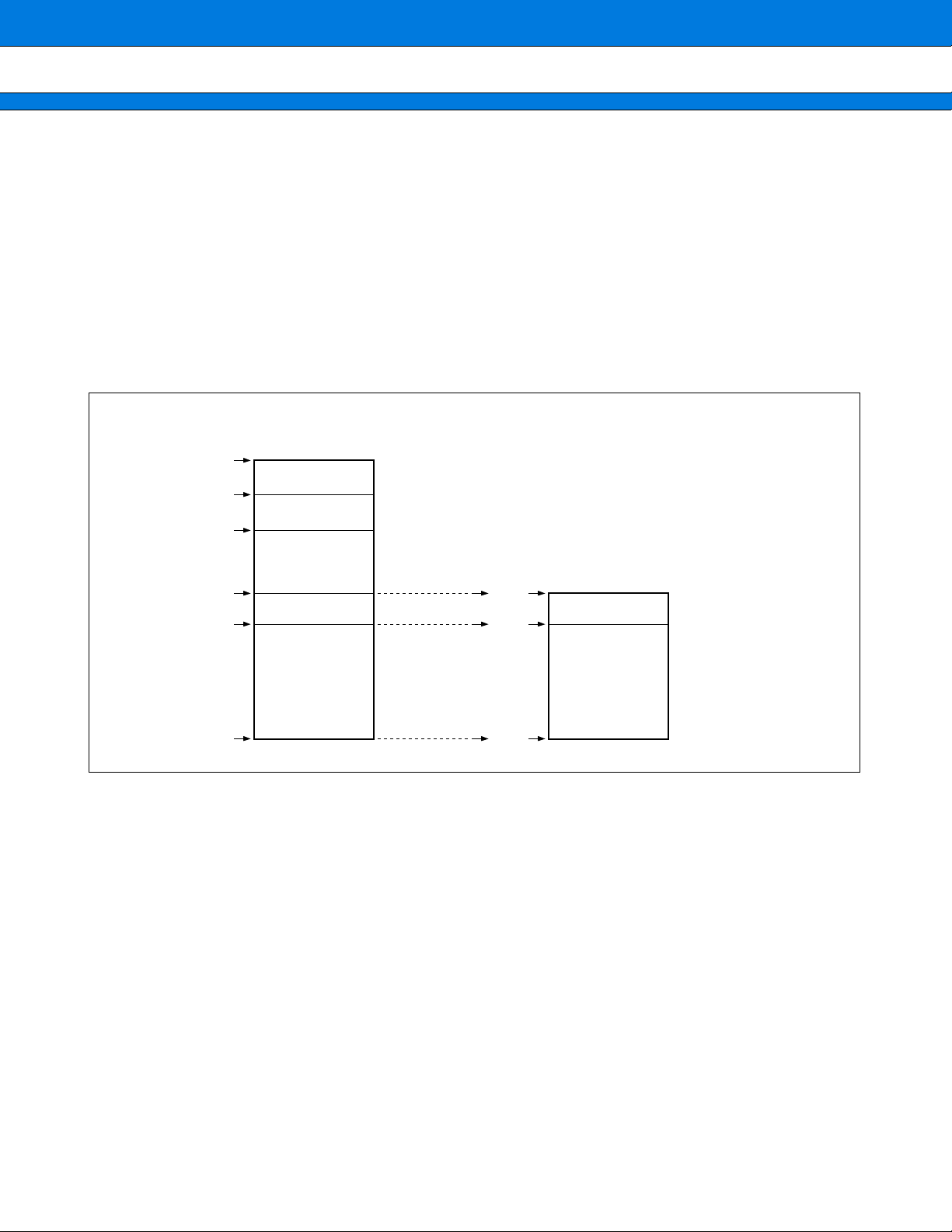
2. Memory Space
Memory space in each mode such as 32-Kbyte PROM, option area is diagrammed below.
• Precautions
(1) The program area of the MB89P647 is 7 bytes smaller than that of the MB89PV640 and MB89647 to provide
an option area. Note this point during program development.
(2) During normal operation, the option data is read when the option area is read from the CPU.
3. Programming to the EPROM
In EPROM mode, the MB89P647 functions equivalent to the MBM27C256A. This allows the PROM to be
programmed with a general-purpose EPROM programmer (the electronic signature mode cannot be used) by
using the dedicated socket adapter.
• Programming procedure
(1) Set the EPROM programmer to the MBM27C256A.
(2) Load program data into the EPROM programmer at 0007
H to 7FFFH (note that addresses 8007H to FFFFH
while operating as internal ROM mode assign to 0007H to 7FFFH in EPROM mode).
Load option data into addresses 0000H to 0006H of the EPROM programmer. (For information about each
corresponding option, see “7. Setting OTPROM Options.”)
(3) Program with the EPROM programmer.
0000H
0080H
0180H
8000H
FFFFH
I/O
RAM
Not available
PROM
32 KB
0000H
7FFFH
EPROM
32 KB
Option area
Single chipAddress EPROM mode
(Corresponding addresses on the EPROM programmer)
8007H 0007H
Not available

17
MB89640 Series
4. Recommended Screening Conditions
High-temperature aging is recommended as the pre-assembly screening procedure f or a product with a blanked
OTPROM microcomputer program.
5. Programming Yield
All bits cannot be programmed at Fujitsu shipping test to a blank ed O TPR OM microcomputer, due to its nature.
For this reason, a programming yield of 100% cannot be assured at all times.
6. EPROM Programmer Socket Adapter
Inquiry: Sun Hayato Co., Ltd.: TEL 81-3-3802-5760
Note: Depending on the EPR OM programmer , inserting a capacitor of about 0.1 µF between V
PP and VSS or VCC
and VSS can stabilize programming operations.
Package Compatible socket adapter
FPT-80P-M06 R OM-80QF-28DP-8L2
FPT-80P-M11 R OM-80QF2-28DP-8L
Program, verify
Aging
+150°C, 48 Hrs.
Data verification
Assembly

18
MB89640 Series
7. Setting OTPROM Options
The programming procedure is the same as that for the PROM. Options can be set by programming values at
the addresses shown on the memory map. The relationship between bits and options is shown on the f ollowing
bit map:
• OTPROM option bit map
Notes:
• Set each bit to 1 to erase.
• Do not write 0 to the vacant bit.
The read value of the vacant bit is 1, unless 0 is written to it.
Bit 7 Bit 6 Bit 5 Bit 4 Bit 3 Bit 2 Bit 1 Bit 0
0000
H
Vacancy
Readable and
writable
Vacancy
Readable and
writable
Vacancy
Readable and
writable
Single/dual-
clock system
1: Dual clock
2: Single clock
Reset pin
output
1: Yes
2: No
Power-on
reset
1: Yes
2: No
Oscillation stabilization time
00: 2
4
/FCH
01: 2
17
/FCH
10: 2
14
/FCH
11: 2
18
/FCH
0001
H
P07
Pull-up
1: No
0: Yes
P06
Pull-up
1: No
0: Yes
P05
Pull-up
1: No
0: Yes
P04
Pull-up
1: No
0: Yes
P03
Pull-up
1: No
0: Yes
P02
Pull-up
1: No
0: Yes
P01
Pull-up
1: No
0: Yes
P00
Pull-up
1: No
0: Yes
0002
H
P17
Pull-up
1: No
0: Yes
P16
Pull-up
1: No
0: Yes
P15
Pull-up
1: No
0: Yes
P14
Pull-up
1: No
0: Yes
P13
Pull-up
1: No
0: Yes
P12
Pull-up
1: No
0: Yes
P11
Pull-up
1: No
0: Yes
P10
Pull-up
1: No
0: Yes
0003
H
P37
Pull-up
1: No
0: Yes
P36
Pull-up
1: No
0: Yes
P35
Pull-up
1: No
0: Yes
P34
Pull-up
1: No
0: Yes
P33
Pull-up
1: No
0: Yes
P32
Pull-up
1: No
0: Yes
P31
Pull-up
1: No
0: Yes
P30
Pull-up
1: No
0: Yes
0004
H
P67
Pull-up
1: No
0: Yes
P66
Pull-up
1: No
0: Yes
P65
Pull-up
1: No
0: Yes
P64
Pull-up
1: No
0: Yes
P63
Pull-up
1: No
0: Yes
P62
Pull-up
1: No
0: Yes
P61
Pull-up
1: No
0: Yes
P60
Pull-up
1: No
0: Yes
0005
H
Vacancy
Readable and
writable
Vacancy
Readable and
writable
Vacancy
Readable and
writable
P74
Pull-up
1: No
0: Yes
P73
Pull-up
1: No
0: Yes
P72
Pull-up
1: No
0: Yes
P71
Pull-up
1: No
0: Yes
P70
Pull-up
1: No
0: Yes
0006
H
Vacancy
Readable and
writable
Vacancy
Readable and
writable
Vacancy
Readable and
writable
Vacancy
Readable and
writable
P83
Pull-up
1: No
0: Yes
P82
Pull-up
1: No
0: Yes
P81
Pull-up
1: No
0: Yes
P80
Pull-up
1: No
0: Yes
 Loading...