


 Loading...
|
|
|
|
|
|
FUJITSU SEMICONDUCTOR |
|
DS07-13712-4E |
|
|
DATA SHEET |
|
|
|
|
|
|
|
|
|
|
|
|
|
|
|
|
|
|
|
|
|
|
|
16-Bit Proprietary Microcontroller
CMOS
F2MC-16LX MB90470 Series
MB90473/474/477/478/F474L/F474H
■ DESCRIPTIONS
The FUJITSU MB90470 Series is a 16-bit general-purpose microcontroller designed for consumer products and other process control applications requiring high-speed and real-time processing.
The F2MC-16LX CPU core instruction set retains the AT architecture of the F2MC*1 family, with additional instructions for use with high-level languages, expanded addressing mode, enhanced multiply and divide instructions, and full bit processing. Also included is a built-in 32-bit accumulator for long-word processing.
Peripheral resources built into the MB90470 series include 8/16-bit PPG, expanded I/O serial interface, UART, 10-bit A/D converter, 16-bit input-output timer, 8/16-bit up-counter, PWC timer, I2C*2 interface, DTP/external interrupt, chip select, and 16-bit reload timer.
*1 : F2MC is an abbreviation for FUJITSU Flexible Microcontroller, and is a registered trademark of FUJITSU, Ltd.
*2 : I2C license :
This product includes licensing of Philips I2C patents if used by the customer in an I2C system subject to the I2C standard specifications established by Philips.
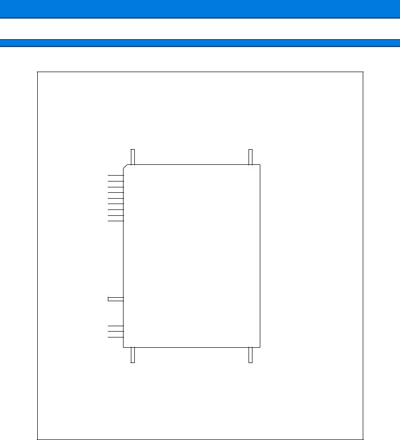
■ PACKAGES
100-pin plastic QFP |
100-pin plastic LQFP |
(FPT-100P-M06) |
(FPT-100P-M05) |

MB90470 Series
■FEATURES
•Clocks
Minimum instruction execution time :
50.0ns at 5 MHz base oscillation with 4 × multiplier (internal operation at 20 MHz/3.3 V ± 0.3 V)
62.5ns at 4 MHz base oscillation with 4 × multiplier (internal operation at 16 MHz/3.0 V ± 0.3 V) Uses PLL clock multiplier.
•Maximum memory size
16Mbytes
•Instruction set optimized for control applications
Handles bit, byte, word, long-word data
23standard addressing modes
32-bit accumulator for enhanced high-precision calculation Signed multiply-divide and expanded RETI instructions
•Instruction system compatible with high-level language (C) multitasking
System stack pointer
Instruction set correlation and barrel shift instructions
•Non-multi bus or multi-bus compatible
•Program patch function (for two address pointers)
•Improved execution speed
4-byte queue
•Powerful interrupt functions
8external interrupt functions with 8-level programmable priority
•Data transfer functions ( DMA or Extended intelligent I/O service)
16channels maximum
µDMA maximum assured operation frequency : 16 MHz
Extended intelligent I/O service maximum assured operation frequency : 20 MHz
•Built-in ROM
Flash versions : 256 KB, Mask ROM versions : 128 KB/256 KB
•Built-in RAM
10KB/16 KB
•General purpose ports
84ports maximum
(includes 16 ports with input pull-up resistance setting, 14 ports with output open drain setting)
•A/D converter
RC sequential comparator type, 8 channels
10-bit resolution, conversion time 4.65 µs (at 20 MHz operation)
•I2C interface
1channel
•PG
1channel
•UART
1channel
•I/O expansion serial interface (SIO)
2channels
•8/16-bit up/down timer
1channel
•16-bit PWC
3channels (including 2-channel input comparison function)
(Continued)
2

MB90470 Series
(Continued)
•16-bit reload timer
1 channel (8-bit × 2-channel, 16-bit × 1-channel mode switching function provided)
•16-bit input-output timer
2-channel input capture, 6-channel output compare, 1-channel free run timer
•2 built-in clock generator systems
•Low power modes
Stop, sleep, CPU intermittent mode, watch mode, etc.
•Package options
QFP100/LQFP100
•Process
CMOS technology
•Supply voltage
Can operate on 3 V single supply systems (with 5 V interface provided by some pins with 3/5 V dual-supply capability)
3

MB90470 Series
■ PRODUCT LINEUP
Parameter |
Part number |
MB90F474L |
|
MB90F474H |
MB90473 |
MB90474 |
|
|
|||||
|
|
|
|
|
|
|
|
|
|
|
|
|
|
ROM capacity |
|
FLASH 256 KB |
|
FLASH 256 KB |
MASKROM |
MASKROM |
|
|
128 KB |
256 KB |
|||
|
|
|
|
|
||
|
|
|
|
|
|
|
RAM capacity |
|
16 KB |
|
16 KB |
10 KB |
16 KB |
|
|
|
|
|
|
|
|
|
Basic instructions |
|
: 351 |
|
|
|
|
Instruction bit length |
|
: 8-bit, 16-bit |
|
|
CPU functions |
|
Instruction length |
|
: 1 byte to 7 bytes |
|
|
|
|
Data bit length |
|
: 1-bit, 8-bit, 16-bit |
|
|
|
|
Minimum instruction execution time |
: 62.5 ns (with 16 MHz machine clock) |
|||
General purpose input/output ports : 84 Max
Ports
General purpose input/output ports (CMOS output)
General purpose input/output ports (built-in pull-up resistance)
General purpose input/output ports (N-ch open drain)
UART |
|
Stop-start synchronized : 1 channel |
|
|
||
8/16-bit PPG timer |
8-bit 6-channel/16-bit 3-channel |
|
|
|||
|
|
|
|
|||
8/16-bit up-down counter/timer |
Two 8-bit up-down counters with 6 event input pins |
|
||||
Two 8-bit reload/compare registers |
|
|
||||
|
|
|
|
|||
|
|
|
|
|
|
|
16-bit |
16-bit free-run timer |
Channel : 1 |
|
|
|
|
Overflow interrupt |
|
|
|
|||
|
|
|
|
|||
input/ |
|
|
|
|
|
|
Output compare (OCU) |
Channels : 6 |
|
|
|
||
out- |
|
|
|
|||
Pin input source : from compare register match signal |
|
|||||
put |
|
|
||||
|
|
|
|
|
||
|
Channels : 2 |
|
|
|
||
timers |
Input capture (ICU) |
|
|
|
||
Register rewritten from pin input (rising/falling/both edges) |
|
|||||
|
|
|
||||
|
|
|
|
|
|
|
DTP/external interrupt circuit |
External interrupt pins : 8 channels (set to edge or level correlation) |
|||||
|
|
|
|
|
||
I/O expansion serial interface |
2-channel, built-in |
|
|
|
||
|
|
|
|
|
||
I2C interface |
1-channel, built-in |
|
|
|
||
|
|
18-bit counter |
|
|
|
|
Time base timer |
Interrupt cycle : 1.0 ms, 4.1 ms, 16.4 ms, 131.1 ms |
|
||||
|
|
(minimum times, at base oscillator frequency 4 MHz) |
|
|||
|
|
|
|
|||
|
|
Conversion accuracy : 8/10-bit switchable |
|
|||
|
|
Single conversion mode (converts selected channel 1 time only) |
||||
A/D converter |
Scan conversion mode |
|
|
|||
(converts multiple consecutive channels, programmable up to 8 channels) |
||||||
|
|
|||||
|
|
Continuous conversion mode (converts selected channels continuously) |
||||
|
|
Stop conversion mode (converts selected channel, stops and repeats) |
||||
|
|
|
|
|||
Watchdog timer |
Reset interval : 3.58 ms, 14.33 ms, 57.23 ms, 458.75 ms |
|
||||
(minimum times, at base oscillator frequency 4 MHz) |
|
|||||
|
|
|
||||
|
|
|
||||
Low power (standby) modes |
Sleep, stop, CPU intermittent, watch mode |
|
||||
|
|
|
|
|
||
Process |
CMOS |
|
|
|
||
|
|
|
|
|
|
|
|
|
Flash model, low |
Flash model, high |
|
|
|
Notes |
|
voltage version |
voltage version |
Mask version |
Mask version |
|
|
(f = 10 MHz or |
|||||
|
|
(f = 20 MHz) |
|
|
||
|
|
less at VCC = 2.4 V) |
|
|
||
|
|
|
|
|
||
|
|
|
|
|
||
Emulator dedicated power supply |
|
|
|
|
||
(Continued)
4

MB90470 Series
(Continued)
|
|
Part number |
MB90477 |
MB90478 |
|
MB90V470B |
|
Parameter |
|
||||||
|
|
|
|
||||
|
|
|
|
|
|
|
|
ROM capacity |
MASKROM |
MASKROM |
|
|
|||
256 KB |
256 KB |
|
|||||
|
|
|
|
|
|||
|
|
|
|
|
|||
RAM capacity |
8 KB |
8 KB |
|
16 KB |
|||
|
|
|
|
|
|
|
|
|
|
|
Basic instructions |
|
: 351 |
|
|
|
|
|
|
: 8-bit, 16-bit |
|||
|
|
|
Instruction bit length |
|
|||
|
|
|
|
: 1 byte to 7 bytes |
|||
CPU functions |
Instruction length |
|
|||||
|
: 1-bit, 8-bit, 16-bit |
||||||
|
|
|
Data bit length |
|
|||
|
|
|
|
: 50 ns (with 20 MHz |
|||
|
|
|
Minimum instruction execution time |
||||
|
|
|
machine clock) |
||||
|
|
|
|
|
|||
|
|
|
|
|
|
||
|
|
|
General purpose input/output ports : 84 Max |
|
|
||
Ports |
|
General purpose input/output ports (CMOS output) |
|
||||
|
General purpose input/output ports (built-in pull-up resistance) |
||||||
|
|
|
|||||
|
|
|
General purpose input/output ports (N-ch open drain) |
|
|||
|
|
|
|
|
|||
UART |
|
Stop-start synchronized : 1 channel |
|
|
|||
|
|
|
|
||||
8/16-bit PPG timer |
8-bit 6-channel/16-bit 3-channel |
|
|
||||
|
|
|
|
|
|||
8/16-bit up-down counter/timer |
Two 8-bit up-down counters with 6 event input pins |
|
|||||
Two 8-bit reload/compare registers |
|
|
|||||
|
|
|
|
|
|||
|
|
|
|
|
|
|
|
|
|
16-bit free-run timer |
Channel : 1 |
|
|
|
|
16-bit |
|
Overflow interrupt |
|
|
|
||
|
|
|
|
|
|||
|
|
|
|
|
|
||
input/ |
|
Output compare (OCU) |
Channels : 6 |
|
|
|
|
output |
|
Pin input source : from compare register match signal |
|
||||
timers |
|
|
|
|
|
|
|
|
Input capture (ICU) |
Channels : 2 |
|
|
|
||
|
|
|
|
|
|||
|
|
Register rewritten from pin input (rising/falling/both edges) |
|||||
|
|
|
|||||
|
|
|
|
|
|||
DTP/external interrupt circuit |
External interrupt pins : 8 channels (set to edge or level correlation) |
||||||
|
|
|
|
|
|||
I/O expansion serial interface |
2-channel, built-in |
|
|
|
|||
|
|
|
|
|
|||
I2C interface |
1-channel, built-in |
|
|
|
|||
|
|
|
18-bit counter |
|
|
|
|
Time base timer |
Interrupt cycle : 1.0 ms, 4.1 ms, 16.4 ms, 131.1 ms |
|
|||||
|
|
|
(minimum times, at base oscillator frequency 4 MHz) |
|
|||
|
|
|
|
|
|
||
|
|
|
Conversion accuracy : 8/10-bit switchable |
|
|
||
|
|
|
Single conversion mode (converts selected channel 1 time only) |
||||
A/D converter |
Scan conversion mode |
|
|
|
|||
(converts multiple consecutive channels, programmable up to 8 channels) |
|||||||
|
|
|
|||||
|
|
|
Continuous conversion mode (converts selected channels continuously) |
||||
|
|
|
Stop conversion mode (converts selected channel, stops and repeats) |
||||
|
|
|
|
||||
Watchdog timer |
Reset interval : 3.58 ms, 14.33 ms, 57.23 ms, 458.75 ms |
||||||
(minimum times, at base oscillator frequency 4 MHz) |
|
||||||
|
|
|
|
||||
|
|
|
|
||||
Low power (standby) modes |
Sleep, stop, CPU intermittent, watch mode |
|
|
||||
|
|
|
|
|
|
||
Process |
|
CMOS |
|
|
|
||
|
|
|
|
|
|
|
|
|
|
|
|
Mask version without |
|
EVA function |
|
Notes |
|
Mask version |
I2C |
|
|||
|
|
User pin |
|||||
|
|
|
|
built-in interface |
|
||
|
|
|
|
|
|
||
|
|
|
|
|
|||
Emulator dedicated power supply |
|
|
|
Included |
|||
|
|
|
|
|
|
|
|
5
MB90470 Series
■ PIN ASSIGNMENTS
(TOP VIEW)
P20/A16 
P21/A17 

P22/A18 
P23/A19 

P24/A20/PPG0 
P25/A21/PPG1 
 P26/A22/PPG2
 P27/A23/PPG3

P30/A00/AIN0 
P31/A01/BIN0 
 VSS
VSS 

P32/A02/ZIN0 
P33/A03/AIN1 
 P34/A04/BIN1

P35/A05/ZIN1  P36/A06/PWC0
P37/A07/PWC1 
 P40/A08/SIN2

P41/A09/SOT2  P42/A10/SCK2
P43/A11/MT00 
 P44/A12/MT01

VCC5
P45/A13/EXTC 
 P46/A14/OUT4
 P47/A15/OUT5

P70/SIN0 
P71/SOT0 

P72/SCK0 

P73/TIN0 

1
2
3
4
5
6
7
8
9
10
11
12
13
14
15
16
17
18
19
20
21
22
23
24
25
26
27
28
29
30
100 P17/AD15/D15
P74/TOT0 31
P16/AD14/D14 |
P15/AD13/D13 |
P14/AD12/D12 |
P13/AD11/D11 |
P12/AD10/D10 |
P11/AD09/D09 |
P10/AD08/D08 |
P07/AD07/D07 |
P06/AD06/D06 |
P05/AD05/D05 |
P04/AD04/D04 |
P03/AD03/D03 |
P02/AD02/D02 |
P01/AD01/D01 |
P00/AD00/D00 |
VCC3 |
X1 X0 |
||||||||||||||||||||
|
|
|
|
|
|
|
|
|
|
|
|
|
|
|
|
|
|
|
|
|
|
|
|
|
|
|
|
|
|
|
|
|
|
|
|
|
|
|
|
|
|
|
|
|
|
|
|
|
|
|
|
|
|
|
|
|
|
|
|
|
|
|
|
|
|
|
|
|
|
|
|
|
|
99 |
98 |
97 |
96 |
95 |
94 |
93 |
92 |
91 |
90 |
89 |
88 |
87 |
86 |
85 |
84 |
83 |
82 |
|||||||||||||||||||
32 |
33 |
34 |
35 |
36 |
37 |
38 |
39 |
40 |
41 |
42 |
43 |
44 |
45 |
46 |
47 |
48 |
49 |
|||||||||||||||||||
|
|
|
|
|
|
|
|
|
|
|
|
|
|
|
|
|
|
|
|
|
|
|
|
|
|
|
|
|
|
|
|
|
|
|
|
|
|
|
|
|
|
|
|
|
|
|
|
|
|
|
|
|
|
|
|
|
|
|
|
|
|
|
|
|
|
|
|
|
|
|
|
|
|
P75/PWC2 |
P76/SCL |
P77/SDA |
AVCC |
AVRH |
AVSS |
P60/AN0 |
P61/AN1 |
P62/AN2 |
P63/AN3 |
Vss |
P64/AN4 |
P65/AN5 |
P66/AN6 |
P67/AN7 |
P80/IRQ0 |
P81/IRQ1 |
MD0 |
|||||||||||||||||||
81 VSS
MD1 50
80 |
|
X0A |
79 |
|
X1A |
|
||
78 |
|
P57/CLK |
|
||
77 |
|
RST |
|
||
76 |
|
P56/RDY |
|
||
75 |
|
P55/HAK |
|
||
74 |
|
P54/HRQ |
|
||
73 |
|
P53/WRH |
|
||
72 |
|
P52/WRL |
|
||
71 |
|
P51/RD |
|
||
70 |
|
P50/ALE |
|
||
69 |
|
PA3/OUT3 |
|
||
68 |
|
PA2/OUT2 |
|
||
67 |
|
PA1/OUT1 |
|
||
66 |
|
PA0/OUT0 |
|
||
65 |
|
P97/IN1 |
|
||
64 |
|
P96/IN0 |
|
||
63 |
|
P95/PPG5 |
|
||
62 |
|
P94/PPG4 |
|
||
61 |
|
P93/FRCK/ADTG/CS3 |
|
||
60 |
|
P92/SCK1/CS2 |
|
||
|
||
59 |
|
P91/SOT1/CS1 |
|
||
58 |
|
P90/SIN1/CS0 |
|
||
|
||
57 |
|
P87/IRQ7 |
|
||
|
||
56 |
|
P86/IRQ6 |
|
||
|
||
55 |
|
P85/IRQ5 |
|
||
|
||
54 |
|
P84/IRQ4 |
|
||
53 |
|
P83/IRQ3 |
|
||
|
||
52 |
|
P82/IRQ2 |
|
||
|
||
51 |
|
MD2 |
|
||
|
(FPT-100P-M06)
6

MB90470 Series
(TOP VIEW)
P22/A18
P23/A19
P24/A20/PPG0
P25/A21/PPG1
P26/A22/PPG2
P27/A23/PPG3
P30/A00/AIN0
P31/A01/BIN0
VSS
P32/A02/ZIN0
P33/A03/AIN1
P34/A04/BIN1
P35/A05/ZIN1
P36/A06/PWC0
P37/A07/PWC1
P40/A08/SIN2
P41/A09/SOT2
P42/A10/SCK2
P43/A11/MT00
P44/A12/MT01 VCC5 P45/A13/EXTC P46/A14/OUT4 P47/A15/OUT5 P70/SIN0
1
2
3
4
5
6
7
8
9
10
11
12
13
14
15
16
17
18
19
20
21
22
23
24
25
P21/A17 |
P20/A16 |
P17/AD15/D15 |
P16/AD14/D13 |
P15/AD13/D13 |
P14/AD12/D12 |
P13/AD11/D11 |
P12/AD10/D10 |
P11/AD09/D09 |
P10/AD08/D08 |
P07/AD07/D07 |
P06/AD06/D06 |
P05/AD05/D05 |
P04/AD04/D04 |
P03/AD03/D03 |
P02/AD02/D02 |
P01/AD01/D01 |
P00/AD00/D00 |
VCC3 |
X1 |
X0 |
VSS |
X0A |
||||||||||||||||||||||||||||
|
|
|
|
|
|
|
|
|
|
|
|
|
|
|
|
|
|
|
|
|
|
|
|
|
|
|
|
|
|
|
|
|
|
|
|
|
|
|
|
|
|
|
|
|
|
|
|
|
|
|
|
|
|
|
|
|
|
|
|
|
|
|
|
|
|
|
|
|
|
|
|
|
|
|
|
|
|
|
|
|
|
|
|
|
|
|
|
|
|
|
|
|
|
|
|
|
|
|
|
|
|
100 |
99 |
98 |
97 |
96 |
95 |
94 |
93 |
92 |
91 |
90 |
89 |
88 |
87 |
86 |
85 |
84 |
83 |
82 |
81 |
80 |
79 |
78 |
||||||||||||||||||||||||||||
26 |
27 |
28 |
29 |
30 |
31 |
32 |
33 |
34 |
35 |
36 |
37 |
38 |
39 |
40 |
41 |
42 |
43 |
44 |
45 |
46 |
|
47 |
48 |
||||||||||||||||||||||
|
|
|
|
|
|
|
|
|
|
|
|
|
|
|
|
|
|
|
|
|
|
|
|
|
|
|
|
|
|
|
|
|
|
|
|
|
|
|
|
|
|
|
|
|
|
|
|
|
|
|
|
|
|
|
|
|
|
|
|
|
|
|
|
|
|
|
|
|
|
|
|
|
|
|
|
|
|
|
|
|
|
|
|
|
|
|
|
|
|
|
|
P71/SOT0 |
P72/SCK0 |
P73/TIN0 |
P74/TOT0 |
P75/PWC2 |
P76/SCL |
P77/SDA |
AVCC |
AVRH |
AVSS |
P60/AN0 |
P61/AN1 |
|
P62/AN2 |
|
P63/AN3 |
VSS |
|
P64/AN4 |
P65/AN5 |
P66/AN6 |
P67/AN7 |
P80/IRQ0 |
P81/IRQ1 |
MD0 |
MD1 |
||||||||||||||||||||
X1A |
P57/CLK |
|
|
|
|
|
|
|
77 |
76 |
|
49 |
50 |
||
|
|
|
|
|
|
|
|
MD2 |
P82/IRQ2 |
||
75
74
73
72
71
70
69
68
67
66
65
64
63
62
61
60
59
58
57
56
55
54
53
52
51
RST
P56/RDY
P55/HAK
P54/HRQ
P53/WRH
P52/WRL
P51/RD
P50/ALE
PA3/OUT3
PA2/OUT2
PA1/OUT1
PA0/OUT0
P97/IN1
P96/IN0
P95/PPG5
P94/PPG4
P93/FRCK/ADTG/CS3
P92/SCK1/CS2
P91/SOT1/CS1
P90/SIN1/CS0
P87/IRQ7
P86/IRQ6
P85/IRQ5
P84/IRQ4
P83/IRQ3
(FPT-100P-M05)
7

MB90470 Series
■ PIN DESCRIPTION
Pin no. |
Pin name |
Circuit |
Description |
||||
LQFP |
QFP |
type |
|||||
|
|
|
|
||||
|
|
|
|
|
|
||
80 |
82 |
|
X0 |
A |
Oscillator pin |
||
|
|
|
|
|
|
||
81 |
83 |
|
X1 |
A |
Oscillator pin |
||
|
|
|
|
|
|
||
78 |
80 |
|
X0A |
A |
32 kHz oscillator pin |
||
|
|
|
|
|
|
||
77 |
79 |
|
X1A |
A |
32 kHz oscillator pin |
||
|
|
|
|
|
|
|
|
75 |
77 |
|
|
|
B |
Reset input pin |
|
RST |
|||||||
|
|
|
|
|
|
|
|
|
|
|
|
|
|
General purpose input/output ports. Set the pull-up resistance |
|
|
|
P00 to P07 |
|
setting register (RDR0) to add pull-up resistance (RD00-RD07 |
|||
|
|
|
|
|
C |
= “1” ) . (Not valid when set for output) |
|
|
|
|
|
|
|
||
83 to 90 |
85 to 92 |
|
|
|
In multiplex mode, these pins function as external address/ |
||
AD00 to AD07 |
(CMOS) |
||||||
|
|
|
|
|
|
data bus lower input/output pins. |
|
|
|
D00 to D07 |
|
In non-multiplex mode, these pins function as external data |
|||
|
|
|
bus lower output pins. |
||||
|
|
|
|
|
|
||
|
|
|
|
|
|
|
|
|
|
|
|
|
|
General purpose input/output ports. Set the pull-up resistance |
|
|
|
P10 to P17 |
|
setting register (RDR1) to add pull-up resistance (RD10-RD17 |
|||
|
93 to |
|
|
|
C |
= “1” ) . (Not valid when set for output) |
|
|
|
|
|
|
|||
91 to 98 |
|
|
|
In multiplex mode, these pins function as external address/ |
|||
100 |
AD08 to AD15 |
(CMOS) |
|||||
|
data bus higher input/output pins. |
||||||
|
|
|
|
|
|
||
|
|
|
|
|
|
|
|
|
|
D08 to D15 |
|
In non-multiplex mode, these pins function as external data |
|||
|
|
|
bus higher output pins. |
||||
|
|
|
|
|
|
||
|
|
|
|
|
|
|
|
|
|
|
|
|
|
General purpose input/output ports. In external bus mode, pins |
|
|
|
P20 to P23 |
|
for which the corresponding bit in the external address output |
|||
|
|
|
control register (HACR) is “1” function as the general purpose |
||||
|
|
|
|
|
|
||
99 |
|
|
|
|
|
input/output ports. |
|
|
|
|
|
|
|
||
100 |
1 to 4 |
|
|
|
E |
In multiplex mode, pins for which the corresponding bit in the |
|
1 |
A16 to A19 |
(CMOS/H) |
external address output control register (HACR) is “0” function |
||||
|
|||||||
2 |
|
|
|
|
|
as the upper address output pins (A16 to A19) . |
|
|
|
|
|
|
|
|
|
|
|
|
|
|
|
In non-multiplex mode, pins for which the corresponding bit in |
|
|
|
A16 to A19 |
|
the external address output control register (HACR) is “0” |
|||
|
|
|
|
|
|
function as the upper address output pins (A16 to A19) . |
|
|
|
|
|
|
|
|
|
|
|
|
|
|
|
General purpose input/output ports. In external bus mode, pins |
|
|
|
P24 to P27 |
|
for which the corresponding bit in the external address output |
|||
|
|
|
control register (HACR) is “1” function as the general purpose |
||||
|
|
|
|
|
|
||
|
|
|
|
|
|
input/output ports. |
|
|
|
|
|
|
|
|
|
|
|
|
|
|
E |
In multiplex mode, pins for which the corresponding bit in the |
|
3 to 6 |
5 to 8 |
A20 to A23 |
external address output control register (HACR) is “0” function |
||||
(CMOS/H) |
|||||||
|
|
|
|
|
as the upper address output pins (A20 to A23) . |
||
|
|
|
|
|
|
|
|
|
|
|
|
|
|
In non-multiplex mode, pins for which the corresponding bit in |
|
|
|
A20 to A23 |
|
the external address output control register (HACR) is “0” |
|||
|
|
|
|
|
|
function as the upper address output pins (A20 to A23) . |
|
|
|
|
|
|
|||
|
|
PPG0 to PPG3 |
|
PPG timer output pins. |
|||
|
|
|
|
|
|
|
|
(Continued)
LQFP : FPT-100P-M05 package QFP : FPT-100P-M06 package
8

MB90470 Series
|
|
|
|
|
|
|
|
|
|
|
|
|
|
|
Pin no. |
Pin name |
Circuit |
Description |
|
|
|
|
|
|
|||
|
LQFP |
QFP |
type |
|
||
|
|
|
|
|||
|
|
|
|
|
||
|
|
|
|
|
|
|
|
|
|
P30 |
|
General purpose input/output port. |
|
|
|
|
|
|
|
|
|
7 |
9 |
A00 |
E |
In non-multibus bus mode, this pin functions as an external |
|
|
(CMOS/H) |
address pin. |
|
|||
|
|
|
|
|
||
|
|
|
|
|
|
|
|
|
|
AIN0 |
|
8/16-bit up-down timer input pin. (ch0) |
|
|
|
|
|
|
|
|
|
|
|
P31 |
|
General purpose input/output port. |
|
|
|
|
|
|
|
|
|
8 |
10 |
A01 |
E |
In non-multibus bus mode, this pin functions as an external |
|
|
(CMOS/H) |
address pin. |
|
|||
|
|
|
|
|
||
|
|
|
|
|
|
|
|
|
|
BIN0 |
|
8/16-bit up-down timer input pin. (ch0) |
|
|
|
|
|
|
|
|
|
|
|
P32 |
|
General purpose input/output port. |
|
|
|
|
|
|
|
|
|
10 |
12 |
A02 |
E |
In non-multibus bus mode, this pin functions as an external |
|
|
(CMOS/H) |
address pin. |
|
|||
|
|
|
|
|
||
|
|
|
|
|
|
|
|
|
|
ZIN0 |
|
8/16-bit up-down timer input pin. (ch0) |
|
|
|
|
|
|
|
|
|
|
|
P33 |
|
General purpose input/output port. |
|
|
|
|
|
|
|
|
|
11 |
13 |
A03 |
E |
In non-multibus bus mode, this pin functions as an external |
|
|
(CMOS/H) |
address pin. |
|
|||
|
|
|
|
|
||
|
|
|
|
|
|
|
|
|
|
AIN1 |
|
8/16-bit up-down timer input pin. (ch1) |
|
|
|
|
|
|
|
|
|
|
|
P34 |
|
General purpose input/output port. |
|
|
|
|
|
|
|
|
|
12 |
14 |
A04 |
E |
In non-multibus bus mode, this pin functions as an external |
|
|
(CMOS/H) |
address pin. |
|
|||
|
|
|
|
|
||
|
|
|
|
|
|
|
|
|
|
BIN1 |
|
8/16-bit up-down timer input pin. (ch1) |
|
|
|
|
|
|
|
|
|
|
|
P35 |
|
General purpose input/output port. |
|
|
|
|
|
|
|
|
|
13 |
15 |
A05 |
E |
In non-multibus bus mode, this pin functions as an external |
|
|
(CMOS/H) |
address pin. |
|
|||
|
|
|
|
|
||
|
|
|
|
|
|
|
|
|
|
ZIN1 |
|
8/16-bit up-down timer input pin. (ch1) |
|
|
|
|
|
|
|
|
|
|
|
P36, P37 |
|
General purpose input/output ports. |
|
|
|
|
|
|
|
|
|
14 |
16 |
A06, A07 |
E |
In non-multibus bus mode, this pin functions as an external |
|
|
15 |
17 |
(CMOS/H) |
address pin. |
|
|
|
|
|
||||
|
|
|
|
|
|
|
|
|
|
PWC0, PWC1 |
|
Functions as PWC input pin. |
|
|
|
|
|
|
|
|
|
|
|
P40 |
|
General purpose input/output port. |
|
|
|
|
|
|
|
|
|
16 |
18 |
A08 |
G |
In non-multibus bus mode, this pin functions as an external |
|
|
(CMOS/H) |
address pin. |
|
|||
|
|
|
|
|
||
|
|
|
|
|
|
|
|
|
|
SIN2 |
|
Single serial I/O input pin |
|
|
|
|
|
|
|
|
|
|
|
P41 |
|
General purpose input/output port. |
|
|
|
|
|
|
|
|
|
17 |
19 |
A09 |
F |
In non-multibus bus mode, this pin functions as an external |
|
|
(CMOS) |
address pin. |
|
|||
|
|
|
|
|
||
|
|
|
|
|
|
|
|
|
|
SOT2 |
|
Single serial I/O output pin |
|
|
|
|
|
|
|
|
(Continued)
LQFP : FPT-100P-M05 package QFP : FPT-100P-M06 package
9

MB90470 Series
|
|
|
|
|
|
|
|
|
|
|
|
|
|
|
|
|
|
|
|
|
|
|
|
|
|
|
|
|
|
|
|
|
|
|
|
|
|
|
|
|
|
|
|
|
Pin no. |
Pin name |
Circuit |
|
|
|
|
|
|
Description |
|
||||||||||
|
|
|
|
|
|
|
|
|
|
||||||||||||
|
LQFP |
QFP |
type |
|
|
|
|
|
|
|
|||||||||||
|
|
|
|
|
|
|
|
|
|
|
|
|
|
|
|
|
|
|
|||
|
|
|
|
|
|
|
|
|
|
|
|
|
|
|
|
|
|
|
|
||
|
|
|
|
|
|
|
|
||||||||||||||
|
|
|
|
P42 |
|
General purpose input/output port. |
|
||||||||||||||
|
|
|
|
|
|
|
|
|
|
|
|||||||||||
|
18 |
20 |
|
A10 |
G |
In non-multibus bus mode, this pin functions as an external |
|
||||||||||||||
|
|
(CMOS/H) |
address pin. |
|
|||||||||||||||||
|
|
|
|
|
|
|
|
|
|||||||||||||
|
|
|
|
|
|
|
|||||||||||||||
|
|
|
SCK2 |
|
Single serial I/O clock input/output pin |
|
|||||||||||||||
|
|
|
|
|
|
|
|||||||||||||||
|
|
|
P43, P44 |
|
General purpose input/output ports. |
|
|||||||||||||||
|
|
|
|
|
|
|
|
|
|
|
|||||||||||
|
19 |
21 |
A11, A12 |
F |
In non-multibus bus mode, this pin functions as an external |
|
|||||||||||||||
|
20 |
22 |
(CMOS) |
address pin. |
|
||||||||||||||||
|
|
|
|
|
|
|
|||||||||||||||
|
|
|
|
|
|
|
|||||||||||||||
|
|
|
MT00, MT01 |
|
PG input pins |
|
|||||||||||||||
|
|
|
|
|
|
|
|
||||||||||||||
|
|
|
|
P45 |
|
General purpose input/output ports. |
|
||||||||||||||
|
|
|
|
|
|
|
|
|
|
|
|||||||||||
|
22 |
24 |
|
A13 |
G |
In non-multibus bus mode, this pin functions as an external |
|
||||||||||||||
|
|
(CMOS/H) |
address pin. |
|
|||||||||||||||||
|
|
|
|
|
|
|
|
|
|||||||||||||
|
|
|
|
|
|
|
|||||||||||||||
|
|
|
EXTC |
|
PG input pin |
|
|||||||||||||||
|
|
|
|
|
|
|
|||||||||||||||
|
|
|
P46, P47 |
|
General purpose input/output ports. |
|
|||||||||||||||
|
|
|
|
|
|
|
|
|
|
|
|||||||||||
|
23 |
25 |
A14, A15 |
F |
In non-multibus bus mode, this pin functions as an external |
|
|||||||||||||||
|
24 |
26 |
(CMOS) |
address pin. |
|
||||||||||||||||
|
|
|
|
|
|
|
|||||||||||||||
|
|
|
|
|
|
|
|||||||||||||||
|
|
|
OUT4/OUT5 |
|
Output compare event output pins |
|
|||||||||||||||
|
|
|
|
|
|
|
|
|
|
|
|||||||||||
|
|
|
|
P50 |
|
General purpose input/output port. In external bus mode, this |
|
||||||||||||||
|
|
|
|
D |
pin functions as the ALE pin |
|
|||||||||||||||
|
68 |
70 |
|
|
|
|
|
|
|||||||||||||
|
|
ALE |
(CMOS) |
In external bus mode, this pin functions as the address load |
|
||||||||||||||||
|
|
|
|
|
|||||||||||||||||
|
|
|
|
|
enable signal (ALE) pin |
|
|||||||||||||||
|
|
|
|
|
|
|
|
|
|
||||||||||||
|
|
|
|
|
|
|
|
|
|
|
|||||||||||
|
|
|
|
P51 |
|
General purpose input/output port. In external bus mode, this |
|
||||||||||||||
|
|
|
|
|
|
|
|
|
|
|
|
|
|
|
|
|
|
||||
|
69 |
71 |
D |
pin functions as the RD pin. |
|
||||||||||||||||
|
|
|
|
|
|
|
|||||||||||||||
|
|
|
|
|
|
(CMOS) |
In external bus mode, this pin functions as the read strobe |
|
|||||||||||||
|
|
|
|
|
|
|
|
|
|||||||||||||
|
|
|
|
|
RD |
||||||||||||||||
|
|
|
|
|
|
|
|
|
|
|
|
|
|
|
|
|
|
|
|||
|
|
|
|
|
|
output (RD) pin. |
|
||||||||||||||
|
|
|
|
|
|
|
|
|
|
||||||||||||
|
|
|
|
|
|
|
|
|
|
|
|||||||||||
|
|
|
|
|
|
|
|
|
General purpose input/output port. In external bus mode, this |
|
|||||||||||
|
|
|
|
P52 |
|
pin functions as the |
WRL |
pin when the WRE bit in the EPCR |
|
||||||||||||
|
|
|
|
|
|
|
|
D |
register is set to “1”. |
|
|||||||||||
|
70 |
72 |
|
|
|
|
|
|
|
|
|
|
|
|
|
|
|
|
|
|
|
|
|
|
|
|
|
In external bus mode, this pin functions as the lower data write |
|
||||||||||||||
|
|
|
|
|
|
(CMOS) |
|
||||||||||||||
|
|
|
|
|
|
|
|
|
strobe output |
(WRL) |
pin. When the WRE bit in the EPCR |
|
|||||||||
|
|
|
|
WRL |
|
||||||||||||||||
|
|
|
|
|
register is set to “0”,this pin functions as a general purpose |
|
|||||||||||||||
|
|
|
|
|
|
|
|
|
|
||||||||||||
|
|
|
|
|
|
|
|
|
input/output port. |
|
|||||||||||
|
|
|
|
|
|
|
|
|
|
|
|||||||||||
|
|
|
|
|
|
|
|
|
General purpose input/output port. In external bus mode with |
|
|||||||||||
|
|
|
|
P53 |
|
16-bit bus width, this pin functions as the |
WRH |
pin when the |
|
||||||||||||
|
|
|
|
|
|
|
|
D |
WRE bit in the EPCR register is set to “1”. |
|
|||||||||||
|
71 |
73 |
|
|
|
|
|
|
|
|
|
|
|
|
|
|
|
|
|
|
|
|
|
|
|
|
|
In external bus mode with 16-bit bus width, this pin functions |
|
||||||||||||||
|
|
|
|
|
|
(CMOS) |
|
||||||||||||||
|
|
|
|
|
|
|
|
|
as the higher data write strobe output |
(WRH) |
pin. When the |
|
|||||||||
|
|
|
|
WRH |
|
||||||||||||||||
|
|
|
|
|
WRE bit in the EPCR register is set to “0”,this pin functions as |
|
|||||||||||||||
|
|
|
|
|
|
|
|
|
|
||||||||||||
|
|
|
|
|
|
|
|
|
a general purpose input/output port. |
|
|||||||||||
|
|
|
|
|
|
|
|
|
|
|
|
|
|
|
|
|
|
|
|
|
|
(Continued)
LQFP : FPT-100P-M05 package QFP : FPT-100P-M06 package
10
MB90470 Series
|
|
|
|
|
|
|
|
|
|
|
|
|
|
|
|
|
|
|
|
|
|
|
|
|
|
|
Pin no. |
Pin name |
Circuit |
|
|
|
Description |
|
||||
|
LQFP |
QFP |
type |
|
|
|
|
|||||
|
|
|
|
|
|
|
|
|||||
|
|
|
|
|
|
|
|
|
||||
|
|
|
|
|
|
|
General purpose input/output port. In external bus mode, this |
|
||||
|
|
|
|
P54 |
|
pin functions as the HRQ pin when the HDE bit in the EPCR |
|
|||||
|
72 |
74 |
|
|
|
D |
register is set to “1”. |
|
||||
|
|
|
|
(CMOS) |
In external bus mode, this pin functions as the hold request |
|
||||||
|
|
|
|
|
|
|
||||||
|
|
|
HRQ |
|
input (HRQ) pin. When the HDE bit in the EPCR register is set |
|
||||||
|
|
|
|
|
|
|
to “0”,this pin functions as a general purpose input/output port. |
|
||||
|
|
|
|
|
|
|
|
|
||||
|
|
|
|
|
|
|
General purpose input/output port. In external bus mode, this |
|
||||
|
|
|
|
P55 |
|
pin functions as the |
HAK |
pin when the HDE bit in the EPCR |
|
|||
|
|
|
|
|
|
D |
register is set to “1”. |
|
||||
|
73 |
75 |
|
|
|
|
|
|
|
|
|
|
|
|
|
|
In external bus mode, this pin functions as the hold acknowl- |
|
|||||||
|
|
|
|
(CMOS) |
|
|||||||
|
|
|
|
|
|
|
|
|
|
|
|
|
|
|
|
|
|
|
edge output (HAK) pin. When the HDE bit in the EPCR register |
|
|||||
|
|
|
|
|
|
|
|
|||||
|
|
|
|
HAK |
|
|||||||
|
|
|
|
|
is set to “0”,this pin functions as a general purpose input/output |
|
||||||
|
|
|
|
|
|
|
|
|||||
|
|
|
|
|
|
|
port. |
|
||||
|
|
|
|
|
|
|
|
|
||||
|
|
|
|
|
|
|
General purpose input/output port. In external bus mode, this |
|
||||
|
|
|
|
P56 |
|
pin functions as the DRY pin when the RYE bit in the EPCR |
|
|||||
|
74 |
76 |
|
|
|
D |
register is set to “1”. |
|
||||
|
|
|
|
(CMOS) |
In external bus mode, this pin functions as the external ready |
|
||||||
|
|
|
|
|
|
|
||||||
|
|
|
RDY |
|
input (RDY) pin. When the RYE bit in the EPCR register is set |
|
||||||
|
|
|
|
|
|
|
to “0”,this pin functions as a general purpose input/output port. |
|
||||
|
|
|
|
|
|
|
|
|
||||
|
|
|
|
|
|
|
General purpose input/output port. In external bus mode, this |
|
||||
|
|
|
|
P57 |
|
pin functions as the CLK pin when the CKE bit in the EPCR |
|
|||||
|
|
|
|
|
|
D |
register is set to “1”. |
|
||||
|
76 |
78 |
|
|
|
|
|
|
|
|
|
|
|
|
|
|
In external bus mode, this pin functions as the machine cycle |
|
|||||||
|
|
|
|
(CMOS) |
|
|||||||
|
|
|
|
|
|
clock output (CLK) pin. When the CKE bit in the EPCR register |
|
|||||
|
|
|
|
CLK |
|
|
||||||
|
|
|
|
|
is set to “0”,this pin functions as a general purpose input/output |
|
||||||
|
|
|
|
|
|
|
|
|||||
|
|
|
|
|
|
|
port. |
|
||||
|
|
|
|
|
|
|
||||||
|
36 to 39 |
38 to 41 |
P60 to P63 |
H |
General purpose input/output ports. |
|
||||||
|
AN0 to AN3 |
(CMOS) |
Analog input pins. |
|
||||||||
|
|
|
|
|||||||||
|
|
|
|
|
|
|
||||||
|
41 to 44 |
43 to 46 |
P64 to P67 |
H |
General purpose input/output ports. |
|
||||||
|
AN4 to AN7 |
(CMOS) |
Analog input pins. |
|
||||||||
|
|
|
|
|||||||||
|
|
|
|
|
|
|
|
|||||
|
25 |
27 |
|
P70 |
G |
General purpose input/output port. |
|
|||||
|
SIN0 |
(CMOS/H) |
UART data input pin. |
|
||||||||
|
|
|
|
|||||||||
|
|
|
|
|
|
|
|
|||||
|
26 |
28 |
|
P71 |
F |
General purpose input/output port. |
|
|||||
|
SOT0 |
(CMOS) |
UART data output pin. |
|
||||||||
|
|
|
|
|||||||||
|
|
|
|
|
|
|
|
|||||
|
27 |
29 |
|
P72 |
G |
General purpose input/output port. |
|
|||||
|
SCK0 |
(CMOS/H) |
UART clock input pin. |
|
||||||||
|
|
|
|
|||||||||
|
|
|
|
|
|
|
|
|||||
|
28 |
30 |
|
P73 |
G |
General purpose input/output port. |
|
|||||
|
TIN0 |
(CMOS/H) |
16-bit reload timer event input pin. |
|
||||||||
|
|
|
|
|||||||||
|
|
|
|
|
|
|
|
|||||
|
29 |
31 |
|
P74 |
F |
General purpose input/output port. |
|
|||||
|
TOT0 |
(CMOS) |
16-bit reload timer output pin. |
|
||||||||
|
|
|
|
|||||||||
|
|
|
|
|
|
|
|
|
|
|
|
|
(Continued)
LQFP : FPT-100P-M05 package QFP : FPT-100P-M06 package
11

MB90470 Series
|
|
|
|
|
|
|
|
|
|
|
|
|
|
|
|
|
Pin no. |
Pin name |
Circuit |
|
Description |
|
|
|
|
|
|
|
|||
|
LQFP |
QFP |
type |
|
|
||
|
|
|
|
|
|||
|
|
|
|
|
|
||
|
|
|
|
|
|
|
|
|
30 |
32 |
P75 |
G |
General purpose input/output port. |
|
|
|
PWC2 |
(CMOS/H) |
PWC input pin. |
|
|||
|
|
|
|
||||
|
|
|
|
|
|
|
|
|
|
|
P76 |
I |
General purpose input/output port. |
|
|
|
31 |
33 |
|
|
|
|
|
|
|
2 |
2 |
|
|||
|
SCL |
(NMOS/H) |
|
||||
|
|
|
I C interface data input/output pin. During I C interface |
|
|||
|
|
|
|
|
operation, the port output should be set to High-Z level. |
|
|
|
|
|
|
|
|
|
|
|
|
|
P77 |
I |
General purpose input/output port. |
|
|
|
32 |
34 |
|
|
|
|
|
|
|
2 |
2 |
|
|||
|
SDA |
(NMOS/H) |
|
||||
|
|
|
I |
C interface clock input/output pin. During I C interface |
|
||
|
|
|
|
|
operation, the port output should be set to High-Z level. |
|
|
|
|
|
|
|
|
|
|
|
45 |
47 |
P80, P81 |
E |
General purpose input/output ports. |
|
|
|
46 |
48 |
IRQ0, IRQ1 |
(CMOS/H) |
External interrupt input pins. |
|
|
|
|
|
|
|
|
|
|
|
50 to 55 |
52 to 57 |
P82 to P87 |
E |
General purpose input/output ports. |
|
|
|
IRQ2 to IRQ7 |
(CMOS/H) |
External interrupt input pins. |
|
|||
|
|
|
|
||||
|
|
|
|
|
|
|
|
|
|
|
P90 |
E |
General purpose input/output port. |
|
|
|
|
|
|
|
|
|
|
|
56 |
58 |
SIN1 |
Single serial I/O data input pin. |
|
||
|
(CMOS/H) |
|
|||||
|
|
|
CS0 |
|
Chip select 0. |
|
|
|
|
|
|
|
|
|
|
|
|
|
P91 |
D |
General purpose input/output port. |
|
|
|
|
|
|
|
|
|
|
|
57 |
59 |
SOT1 |
Single serial I/O data output pin. |
|
||
|
(CMOS) |
|
|||||
|
|
|
|
|
|
|
|
|
|
|
CS1 |
|
Chip select 1. |
|
|
|
|
|
|
|
|
|
|
|
|
|
P92 |
E |
General purpose input/output port. |
|
|
|
|
|
|
|
|
|
|
|
58 |
60 |
SCK1 |
Single serial I/O clock input/output pin. |
|
||
|
(CMOS/H) |
|
|||||
|
|
|
CS2 |
|
Chip select 2. |
|
|
|
|
|
|
|
|
|
|
|
|
|
P93 |
|
General purpose input/output port. |
|
|
|
|
|
|
|
|
|
|
|
|
|
FRCK |
|
In free run timer operation, this pin functions as the external |
|
|
|
|
|
E |
clock input pin. |
|
||
|
59 |
61 |
|
|
|||
|
ADTG |
(CMOS/H) |
In A/D converter operation, this pin functions as the external |
|
|||
|
|
|
|
||||
|
|
|
|
trigger input pin. |
|
||
|
|
|
|
|
|
||
|
|
|
|
|
|
|
|
|
|
|
CS3 |
|
Chip select 3. |
|
|
|
|
|
|
|
|
|
|
|
60 |
62 |
P94 |
D |
General purpose input/output port. |
|
|
|
PPG4 |
(CMOS) |
PPG timer output pin. |
|
|||
|
|
|
|
||||
|
|
|
|
|
|
|
|
|
61 |
63 |
P95 |
D |
General purpose input/output port. |
|
|
|
PPG5 |
(CMOS) |
PPG timer output pin. |
|
|||
|
|
|
|
||||
|
|
|
|
|
|
|
|
|
62 |
64 |
P96 |
E |
General purpose input/output port. |
|
|
|
IN0 |
(CMOS/H) |
Functions as input capture ch 0 trigger input. |
|
|||
|
|
|
|
||||
|
|
|
|
|
|
|
|
(Continued)
LQFP : FPT-100P-M05 package QFP : FPT-100P-M06 package
12

MB90470 Series
(Continued)
Pin no. |
Pin name |
Circuit |
Description |
||
|
|
||||
LQFP |
QFP |
type |
|||
|
|
||||
|
|
|
|||
|
|
|
|
|
|
63 |
65 |
P97 |
E |
General purpose input/output port. |
|
IN1 |
(CMOS/H) |
Functions as input capture ch 1 trigger input. |
|||
|
|
||||
|
|
|
|
|
|
64 to 67 |
66 to 69 |
PA0 to PA3 |
D |
General purpose input/output ports. |
|
OUT0 to OUT3 |
(CMOS) |
Output compare event output pins. |
|||
|
|
||||
|
|
|
|
|
|
33 |
35 |
AVCC |
|
A/D converter power supply pin. |
|
|
|
|
|
|
|
34 |
36 |
AVRH |
|
A/D converter external reference power pin. |
|
|
|
|
|
|
|
35 |
37 |
AVSS |
|
A/D converter power supply pin. |
|
|
|
|
|
|
|
47 to 49 |
49 to 51 |
MD0 to MD2 |
J |
Input pins for specifying operating mode. |
|
(CMOS/H) |
|||||
|
|
|
|
|
|
82 |
84 |
VCC3 |
|
3.3 V ± 0.3 V power supply pin (VCC3) . |
|
|
|
|
|
|
|
21 |
23 |
VCC5 |
|
3.3 V ± 0.3 V/5.0 V ± 0.5 V dual power supply pin (VCC5) . |
|
|
|
|
|
|
|
9 |
11 |
|
|
|
|
40 |
42 |
VSS |
Power supply input pins (GND) . |
||
79 |
81 |
|
|
|
|
|
|
|
|
|
|
LQFP : FPT-100P-M05 package QFP : FPT-100P-M06 package
Notes : • For use as a 3.3 V single supply device, apply the same voltage to the VCC3 and VCC5 power supply pins.
•For use with a dual power supply, apply the respective voltages to the VCC3 and VCC5 power supply pins.
•In use with a dual power supply, a total of 32 pins (P20/A16 to P27/A23/PPG3, P30/A00/AIN0 to P37/ A07/PWC1, P40/A08/SIN2 to P47/A15/OUT5 and P70/SIN0 to P77/SDA) can be used in a 5 V interface. Note that all other pins must be used in 3 V interface.
•In use with a dual power supply, it is not possible to turn on only the 5 V or the 3 V power supply independently. Always turn on both power supplies simultaneously. (It is recommended that the 3 V power to the MB90470 series be turned on first.)
13
MB90470 Series
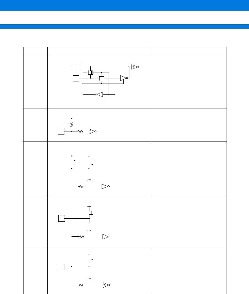
■ I/O CIRCUIT TYPES |
|
|
|
Type |
Circuit |
Remarks |
|
X1, X1A |
|
|
|
|
|
Oscillator feedback resistance : |
|
X0, X0A |
|
X1,X0 |
1 MΩ approx. |
A |
|
X1A,X0A |
10 MΩ approx. |
|
|
||
|
|
Includes standby control |
|
|
|
Standby control |
|
|
|
signal |
|
B |
|
|
|
|
Hysteresis with pull-up resistance |
||
|
|
|
|||||
|
|
HYS |
Input resistance 50 kΩ approx. |
||||
|
|
|
|
|
|
||
|
|
||||||
|
|
|
|
|
|
|
|
|
|
|
|
|
|
|
|
|
|
|
|
|
|
|
|
|
|
|
CTL |
|
|
|
|
|
|
|
|
|
|
|
|
|
|
|
|
|
|
|
|
|
|
|
|
|
|
|
|
||
|
|
|
|
|
|
|
|
|
|
|
|
|
|
|
|
|
|
|
|
|
|
|
|
|
|
|
||
|
|
|
|
|
|
|
|
|
|
|
|
|
|
|
|
|
|
|
|
|
|
|
|
|
|
|
||
|
|
|
|
|
|
|
|
|
|
|
|
|
|
|
|
|
|
|
|
|
|
|
|
|
|
|
|
Includes input pull-up resistance control |
|
|
|
|
|
|
|
|
|
|
|
|
|
|
|
|
|
|
|
|
|
|
|
|
|
|
|
|
|
|
|
|
|
|
|
|
|
|
|
|
|
|
|
|
|
|
|
|
|
|
|
|
|
|
|
|
|
|
C |
|
|
|
|
|
|
|
|
|
|
|
|
|
|
|
|
|
|
|
|
|
|
|
|
|
|
|
CMOS level input/output |
|
|
|
|
|
|
|
|
|
|
|
|
|
|
|
|
|||||||||||||
|
|
|
|
|
|
|
|
|
|
|
|
|
|
|
|
|
|
|
|
|
|
|
|
|
|
|
|
Resistance : 50 kΩ approx. |
|
|
|
|
|
|
|
|
|
|
|
|
|
|
|
|
|
|
|
|
|
||||||||
|
|
|
|
|
|
|
|
|
|
|
|
|
|
|
|
|
|
|
|
|
|
|
||||||
|
|
|
|
|
|
|
|
|
|
|
|
|
|
|
|
|
|
|
|
|
|
|
|
|
|
|
CMOS |
|
|
|
|
|
|
|
|
|
|
|
|
|
|
|
|
|
|
|
|
|
|
|
|
|
|
|
|
||
|
|
|
|
|
|
|
|
|
|
|
|
|
|
|
|
|
|
|
|
|
|
|
|
|
|
|
|
|
|
|
|
|
|
|
|
|
|
|
|
|
|
|
|
|
|
|
|
|
|
|
|
|
|
|
|
|
|
|
|
|
|
|
|
|
|
|
|
|
|
|
|
|
|
|
|
|
|
|
|
|
|
|
|
|
|
|
|
|
|
|
|
|
|
|
|
|
|
|
|
|
|
|
|
|
|
|
|
|
|
|
|
|
|
|
|
|
|
|
|
|
|
|
|
|
|
|
|
|
|
|
|
|
|
|
|
|
|
|
|
|
|
|
|
|
D |
|
|
|
|
CMOS level input/output |
|
|
|
|
|
|||
|
|
|
|
|
|
|
|
|
|
|
|
|
|
CMOS
|
|
|
|
|
|
|
|
|
|
|
|
|
|
|
Hysteresis input |
|
|
|
|
|
|
|
|
|
|
|
|
|
|
|
|
|
|
|
|
|
|
|
|
|
|
|
|
|
|
|
|
|
|
|
|
|
|
|
|
|
|
|
|
|
|
|
|
|
|
|
|
|
|
|
|
|
|
|
|
|
|
|
|
|
|
|
|
|
|
|
|
|
|
|
|
|
|
|
|
|
|
|
|
|
|
|
|
|
|
|
|
|
|
|
|
E |
|
|
|
|
|
|
|
|
|
|
|
||||
|
|
|
|
|
|
|
|
|
|
|
|
|
CMOS level input/output |
||
|
|
|
|
|
|
|
|
|
|
|
|
||||
|
|
|
|
|
|
|
|
|
|
|
|
|
|
|
|
|
|
|
|
|
|
|
|
|
|
|
|
|
|
CMOS |
|
|
|
|
|
|
|
|
|
|
|
|
|
|
|
||
|
|
|
|
|
|
|
|
|
|
|
|
|
|
|
|
|
|
|
|
|
|
|
|
|
|
|
|
|
|
|
|
(Continued)
14

MB90470 Series
(Continued)
Type |
|
|
|
|
Circuit |
Remarks |
|||
|
|
|
|
|
|
|
|
Open drain |
|
|
|
|
|
|
|
|
|
|
|
|
|
|
|
|
|
|
|
|
|
F |
|
|
|
|
|
|
|
control signal |
CMOS level input/output |
|
|
|
|
|
|
|
|
||
|
|
|
|
|
|
|
|
||
|
|
|
|
|
|
|
CMOS |
Includes open drain control |
|
|
|
|
|
|
|
||||
|
|
|
|
|
|
|
|
||
|
|
|
|
|
|
|
|
|
|
|
|
|
|
|
|
|
|
|
|
|
|
|
|
|
|
|
|
|
|
|
|
|
|
|
|
|
|
|
|
|
|
|
|
|
|
|
|
|
|
|
|
Open drain |
|||
|
|
|
|
|
|
|
|
|
|
|
|
|
|
||||
|
|
|
|
|
|
|
|
|
|
|
|
|
|
||||
|
|
|
|
|
|
|
|
|
|
|
|
|
|
control signal |
|||
|
|
|
|
|
|
|
|
|
|
|
|
|
|
|
|
|
CMOS level output |
|
|
|
|
|
|
|
|
|
|
|
|
|
|
|
|||
G |
|
|
|
|
|
|
|
|
|
|
|
|
|
|
|
|
Hysteresis input |
|
|
|
|
|
|
|
|
|
|
|
|
|
|
||||
|
|
|
|
|
|
|
|
|
|
|
|||||||
|
|
|
|
|
|
|
|
|
|
|
|||||||
|
|
|
|
|
|
|
|
|
|
|
|
|
|
|
|
|
Includes open drain control |
|
|
|
|
|
|
|
|
|
|
|
|
|
|
|
|
HYS |
|
|
|
|
|
|
|
|
|
|
|
|
|
|
|
|
|
|
|
|
|
|
|
|
|
|
|
|
|
|
|
|
|
|
|
|
|
|
|
|
|
|
|
|
|
|
|
|
|
|
|
|
|
|
|
|
|
|
|
|
|
|
|
|
|
|
|
|
|
|
|
|
|
|
|
|
|
|
|
|
|
|
|
|
|
|
|
|
|
|
|
H |
CMOS level input/output |
|
Analog input |
||
|
||
CMOS |
|
|
Analog input |
|
|
Digital output |
|
|
I |
Hysteresis input |
|
N-ch open drain output |
||
|
||
HYS |
|
|
(Flash model) |
|
|
|
Flash model |
|
|
CMOS level input |
|
Control signal |
Includes high voltage control for FLASH |
|
test |
||
J |
||
Mode input |
|
|
Spreading resistance |
|
|
(Mask version) |
Mask version |
|
HYS |
||
Hysteresis input port |
15

MB90470 Series
■HANDLING DEVICES
(1)Strictly observe maximum rated voltages (prevent latchup)
When CMOS integrated circuit devices are subjected to applied voltages higher than VCC at input and output pins other than mediumand high-withstand voltage pins, or to voltages lower than VSS, or when voltages in excess of rated levels are applied between VCC and VSS, a phenomenon known as latchup can occur. In a latchup condition, supply current can increase dramatically and may destroy semiconductor elements. In using semiconductor devices, always take sufficient care to avoid exceeding maximum ratings.
Also care must be taken when power to analog systems is switched on or off, to ensure that the analog power supply (AVCC, AVRH) and analog input do not exceed the digital power supply (VCC) .
(2) Treatment of unused pins
If unused input pins are left open, abnormal operation or latchup may cause permanent damage to the semiconductor. Any such pins should be pulled up or pulled down through resistance of at least 2 kΩ.
Also any unused input/output pins should be left open in output status, or if set to input status should be treated in the same way as input pins.
(3) Precautions for use of external clock signals
Even when an external clock is used, a stabilization period is required following a power-on reset or release from sub clock mode or stop mode. Also, when an external clock is used 20 MHz should be used as a guideline for an upper frequency limit.
The following figure shows a sample use of external clock signals.
X0
OPEN X1
(4) Power supply pins
When using multiple VCC/VSS sources, always make sure to design devices with external connections of all power supply pins to supply or ground elements, in order to prevent latchup, reduce unwanted radiation, and prevent abnormal strobe signal operation due to rise in ground level, as well as to maintain total rated output current. In addition, care must be given to connecting the VCC and VSS pins of this device to a current source with as little impedance as possible. It is recommended that a bypass capacitor of 1.0 µF be connected between VCC and VSS as close to the pins as possible.
(5) Crystal oscillator circuits
Abnormal operation of this device can result from noise in the proximity of the X0/X1 and X0A/X1A pins. For stable operation, it is strongly recommended that the printed circuit artwork provide capacitors placed as close as possible between the X0/X1, X0A/X1A and crystal oscillator (or ceramic oscillator) as well as ground, and be wired so as to avoid crossing other wiring wherever possible.
16

MB90470 Series
(6) Precautions for use of external oscillators (crystals)
The target value for the upper limit of oscillator (crystals) frequencies should be 20 MHz. Also, when operating at internal frequencies of 16 MHz, the PLL multiplier should be used.
(7) Proper power-on/off sequence
The A/D converter power (AVCC, AVRH) and analog input (AN0 to AN7) must be turned on after the digital power supply (VCC) is turned on. The A/D converter power (AVCC, AVRH) and analog input (AN0 to AN7) must be shut off before the digital power supply (VCC) is shut off. Care should be taken that AVRH does not exceed AVCC. Even when pins used as analog input pins are doubled as input ports, be sure that the input voltage does not exceed AVCC.
Note : VCC = VCC3 = VCC5
(8) Treatment of A/D converter power supply pins
Even if the A/D converter is not used, pins should be connected so that AVCC = AVRH = VCC, and AVSS = VSS.
(9) Power-on procedures
In order to prevent abnormal operation of the internal built-in step-down circuits, voltage rise during power-on should be attained within 50 s (0.2 V to 2.7 V) .
(10) Stable power supply
Even within the operating range of the VCC supply voltage, rapid changes in supply voltage may cause abnormal operation. As a basis for stable operation, it is recommended that voltage variation be restricted in order to limit VCC ripple fluctuations (P-P values) to 10% at commercial frequencies of 50 Hz to 60 Hz, and transient fluctuations to 0.1 V/ms at instantaneous points such as power switching.
(11) Precautions for use of two power supplies
The MB90470 series usually uses the 3-V power supply as the main power source. With VCC3 = 3 V and VCC5 = 5 V, however, it can interface with P20/A16 to P27/A23/PPG3, P30/A00/AIN0 to P37/A07/PWC1,
P40/A08/SIN2 to P47/A15/OUT5, P70/SIN0 to P77/SDA for the 5-V power supply separetely from the 3-V power supply at all operation mode.
(Caution) The analog power supply for the A/D converter (AVCC, AVSS etc.) can only operate with the 3 V system.
(12) Crystal oscillator circuits during power-saving operation
When the power supply is lower than 2.0 V, the external crystal oscillator may not operate even when power is on. For this reason, the use of an external clock signal is recommended.
(13)Caution : low-voltage flash models (2.4 V to 3.6 V/10 MHz) do not have security functions
(14)Treatment of unused input pins
N.C. (internally connected) pins should always be left open.
(15) When the dual-supply MB90470 series is used as a 1-supply device, use connections so that X0A = VSS, and X1A = Open.
17

MB90470 Series
(16)For serial writing to flash memory, always make sure that the operating voltage VCC is between 3.13 V and 3.6 V.
For normal writing to flash memory, always make sure that the operating voltage VCC is between 3.0 V and 3.6 V.
(17)Caution on Operations during PLL Clock Mode
If the PLL clock mode is selected, the microcontroller attempt to be working with the self-oscillating circuit even when there is no external oscillator or external clock input is stopped. Performance of this operation, however, cannot be guaranteed.
18

MB90470 Series
■ BLOCK DIAGRAM
X0, X1, RST
X0A, X1A
MD2, MD1, MD0
SIN0
SOT0
SCK0
SIN1, SIN2
SOT1, SOT 2  SCK1, SCK2
AVCC
AVRH
AVSS
ADTG
AN0 to AN7
PWC0
PWC1
PWC2
|
|
|
|
|
|
CPU |
|
Clock |
|
|
|
|
|
8 |
|
|
FMC-16LX |
|||
|
|
|||||
|
control circuit |
|
|
series core |
||
|
|
|
|
|
|
|
|
RAM |
|
|
|
|
|
|
|
|
|
|
|
|
|
|
|
|
|
|
|
ROM
µDMA
Communication prescaler 

|
|
|
2 |
|
|
MC2F |
|
|
|
|
|
||
UART |
|
|
|
|||
|
|
|
16LX- |
|||
|
|
|
|
|
|
|
|
|
|
|
|
|
|
|
|
|
|
|
|
|
|
|
|
|
|||
I/O expansion serial |
|
|
|
BUS |
||
|
|
|
|
|||
interface × 2 channels |
|
|
|
|
||
|
|
|
|
|||
A/D converter |
|
|
|
|
||
|
|
|
|
|||
|
|
|
|
|||
(10-bit) |
|
|
|
|
||
|
|
|
|
|
|
|
16-bit PWC
3 channels
Interrupt controller
8/16-bit PPG
8/16-bit up/down counter
µPG
Chip select
Input/output timer
16-bit input capture × 2
16-bit output compare × 6
16-bit free-run timer
16-bit reload timer
I2C interface
External interrupt
I/O ports
8 |
|
8 |
|
8 |
|
8 |
|
8 |
|
8 |
|
8 |
|
8 |
|
8 |
|
8 |
|
4 |
|
|
|
|
|
|
|
|
|
|
|
|
|
|
|
|
|
|
|
|
|
|
|
P00 |
P10 |
P20 |
P30 |
P40 |
P50 |
P60 |
P70 |
P80 |
P90 |
PA0 |
|||||||||||
|
|
|
|
|
|
|
|
|
|
|
|||||||||||
P07 |
P17 |
P27 |
P37 |
P47 |
P57 |
P67 |
P77 |
P87 |
P97 |
PA3 |
|||||||||||
 PPG0, PPG1
 PPG2, PPG3
  PPG4, PPG5
 AIN0, AIN1
 BIN0, BIN1
  ZIN0, ZIN1
 EXTC
EXTC
 MT00
MT00
 MT01
MT01
CS0, CS1,
CS2, CS3
 IN0, IN1
 OUT0, OUT1, OUT2, OUT3, OUT4, OUT5
TIN0
 TOT0
TOT0
 SCL
SCL
 SDA
SDA
8
IRQ0 to IRQ7
P00 to P07 (8 pins) |
: Input pull-up resistance setting register provided. |
P10 to P17 (8 pins) |
: Input pull-up resistance setting register provided. |
P40 to P47 (8 pins) |
: Open drain setting register provided. |
P70 to P75 (6 pins) |
: Open drain setting register provided. |
P76, P77 (2 pins) |
: Open drain |
Note : In the above diagram, I/O ports are shown sharing pin numbers with the built-in function blocks. However pins may not be used as I/O ports when they are in use as pins for build-in function modules.
19

MB90470 Series
■ MEMORY MAP |
|
|
|
|
|
Single chip |
Internal ROM external bus |
External ROM external bus |
|||
FFFFFFH |
|
|
|
|
|
ROM area |
ROM area |
|
|
||
Address 1# |
|
|
|
|
|
010000H |
|
|
|
|
|
ROM area |
ROM area |
|
|
||
FF bank image |
FF bank image |
|
|
||
004000H |
|
|
|
|
|
|
|
|
* |
|
|
Address 2# |
|
|
|
|
|
RAM |
Register |
RAM |
Register |
RAM |
Register |
000100H |
|
|
|
|
|
0000D0H |
|
|
|
|
|
Peripheral |
Peripheral |
Peripheral |
|||
000000H |
|
|
|
|
|
|
: Internal |
: External |
: Access not available |
|
|
* : In models where address 2# coincides with 004000H, there is no external area.
Model |
Address 1# |
Address 2# |
|
|
|
MB90473 |
FE0000H |
002900H |
|
|
|
MB90474 |
FC0000H |
004000H |
|
|
|
MB90477/478 |
FC0000H |
002100H |
|
|
|
MB90F474 |
FC0000H |
004000H |
|
|
|
MB90V470 |
(FC0000H) |
004000H |
|
|
|
The image of FF bank ROM is reflected in the top of the 00 bank, for greater efficiency in using the C compiler for small models. The lower 16-bit address on the FF bank is the same as the lower 16-bit address on the 00 bank, so that it is possible to reference tables in ROM without using the pointer for a far specification.
For example, when accessing 00C000H, it is actually the content of ROM at FFC000H that is accessed. Here, because the ROM area on the FF bank exceeds 48 KB, it is not possible to view the entire area in the image on the 00 bank. Therefore, the image from FF4000H to FFFFFFH is visible on the 00 bank, and FF0000H to FF3FFFH is visible only on the FF bank.
20
MB90470 Series
■F2MC-16L CPU PROGRAMMING MODEL
• Special purpose registers
|
|
|
|
|
|
|
|
|
|
|
|
|
|
|
|
|
|
AH |
|
|
|
|
AL |
Accumulator |
|||||||
|
|
|
|
|
|
|
|
|
|
|
|
|
|
|
|
|
|
|
|
|
|
|
|
|
|||||||
|
|
|
|
|
|
|
USP |
User stack pointer |
|||||||
|
|
|
|
|
|
|
|
|
|||||||
|
|
|
|
|
|
|
SSP |
System stack pointer |
|||||||
|
|
|
|
|
|
|
|
|
|||||||
|
|
|
|
|
|
|
PS |
Processor status |
|||||||
|
|
|
|
|
|
|
|
|
|||||||
|
|
|
|
|
|
|
PC |
Program counter |
|||||||
|
|
|
|
|
|
|
|
|
|
|
|
|
|
|
|
|
|
|
|
|
|
|
|
|
|
|
|
|
|
|
|
|
|
|
|
|
|
|
|
|
|
DPR |
Direct page register |
||||
|
|
|
|
|
|
|
|
|
|
|
|
|
|
|
|
|
|
|
|
|
|
|
|
|
|
|
|
|
|
|
|
|
|
|
|
|
|
|
|
|
|
PCB |
Program bank register |
||||
|
|
|
|
|
|
|
|
|
|
|
|
|
|
|
|
|
|
|
|
|
|
|
|
|
|
DTB |
Data bank register |
||||
|
|
|
|
|
|
|
|
|
|
|
|
|
|
|
|
|
|
|
|
|
|
|
|
|
|
USB |
User stack bank register |
||||
|
|
|
|
|
|
|
|
|
|
|
|
|
|
|
|
|
|
|
|
|
|
|
|
|
|
SSB |
System stack bank register |
||||
|
|
|
|
|
|
|
|
|
|
|
|
|
|
|
|
|
|
|
|
|
|
|
|
|
|
ADB |
Additional data bank register |
||||
|
|
|
|
|
|
|
|
|
|
|
|
|
|
|
|
|
|
|
|
|
|
|
|
|
|
|
|
|
|
|
|
|
|
|
|
|
|
|
|
|
|
|
8 bit |
|
|
|
|
|
|
|
|
|
|
|
|
|
|
|
|
|
|||
|
|
|
|
|
|
|
|
|
|
|
|
|
|
||
|
|
|
|
|
|
|
|
|
|
|
|
|
|
||
|
|
|
|
|
|
|
16 bit |
|
|
|
|
|
|
||
|
|
|
|
|
|
|
|
|
|
|
|
||||
|
|
|
|
|
|
|
|
|
|
||||||
|
|
|
|
|
|
|
|
|
|
|
|
|
|
|
|
|
|
|
32 bit |
|
|
|
|
|
|
|
|
|
|
||
|
|
|
|
|
|||||||||||
|
|
|
|
|
|
|
|
|
|
|
|
|
|
|
|
|
|
|
|
|
|
|
|
|
|
|
|
|
|
|
|
• General purpose registers
MSB |
LSB |
16 bit
000180H + RP × 10H 
 RW0
RW0
RL0
RW1
RW2
|
|
RL1 |
|
|
RW3 |
||
|
|
||
|
|
|
|
R1 |
R0 |
RW4 |
|
|
|
RL2 |
|
R3 |
R2 |
||
RW5 |
|||
|
|
|
|
R5 |
R4 |
RW6 |
|
|
|
RL3 |
|
R7 |
R6 |
||
RW7 |
• Processor status
15 |
|
13 |
12 |
|
8 |
7 |
|
0 |
|
|
|
|
|||||||
PS |
|
ILM |
|
RP |
|
CCR |
|||
|
|
|
|
|
|
|
|
|
|
21

MB90470 Series
■ I/O MAP
Address |
Register name |
Symbol |
Access |
Resource name |
Default |
||
|
|
|
|
|
|
|
|
00H |
Port 0 data register |
PDR0 |
R/W |
Port |
0 |
XXXXXXXX |
|
|
|
|
|
|
|
|
|
01H |
Port 1 data register |
PDR1 |
R/W |
Port |
1 |
XXXXXXXX |
|
|
|
|
|
|
|
|
|
02H |
Port 2 data register |
PDR2 |
R/W |
Port |
2 |
XXXXXXXX |
|
|
|
|
|
|
|
|
|
03H |
Port 3 data register |
PDR3 |
R/W |
Port |
3 |
XXXXXXXX |
|
|
|
|
|
|
|
|
|
04H |
Port 4 data register |
PDR4 |
R/W |
Port |
4 |
XXXXXXXX |
|
|
|
|
|
|
|
|
|
05H |
Port 5 data register |
PDR5 |
R/W |
Port |
5 |
XXXXXXXX |
|
|
|
|
|
|
|
|
|
06H |
Port 6 data register |
PDR6 |
R/W |
Port |
6 |
XXXXXXXX |
|
|
|
|
|
|
|
|
|
07H |
Port 7 data register |
PDR7 |
R/W |
Port |
7 |
1 1XXXXXX |
|
|
|
|
|
|
|
|
|
08H |
Port 8 data register |
PDR8 |
R/W |
Port |
8 |
XXXXXXXX |
|
|
|
|
|
|
|
|
|
09H |
Port 9 data register |
PDR9 |
R/W |
Port |
9 |
XXXXXXXX |
|
|
|
|
|
|
|
||
0AH |
Port A data register |
PDRA |
R/W |
Port A |
- - - - XXXX |
||
|
|
|
|
|
|
||
0BH |
Port 3 timer input enable register |
UDRE |
R/W |
Up/down timer |
XX 0 0 0 0 0 0 |
||
input control |
|||||||
|
|
|
|
|
|||
|
|
|
|
|
|
|
|
0CH |
Interrupt/DTP enable register |
ENIR |
R/W |
|
|
0 0 0 0 0 0 0 0 |
|
|
|
|
|
|
|
||
0DH |
Interrupt/DTP enable register |
EIRR |
R/W |
DTP/external |
0 0 0 0 0 0 0 0 |
||
0EH |
Demand level setting register |
ELVR |
R/W |
interrupt |
0 0 0 0 0 0 0 0 |
||
|
|
|
|
|
|
||
0FH |
Demand level setting register |
R/W |
|
|
0 0 0 0 0 0 0 0 |
||
|
|
|
|||||
|
|
|
|
|
|
|
|
10H |
Port 0 direction register |
DDR0 |
R/W |
Port |
0 |
0 0 0 0 0 0 0 0 |
|
|
|
|
|
|
|
|
|
11H |
Port 1 direction register |
DDR1 |
R/W |
Port |
1 |
0 0 0 0 0 0 0 0 |
|
|
|
|
|
|
|
|
|
12H |
Port 2 direction register |
DDR2 |
R/W |
Port |
2 |
0 0 0 0 0 0 0 0 |
|
|
|
|
|
|
|
|
|
13H |
Port 3 direction register |
DDR3 |
R/W |
Port |
3 |
0 0 0 0 0 0 0 0 |
|
|
|
|
|
|
|
|
|
14H |
Port 4 direction register |
DDR4 |
R/W |
Port |
4 |
0 0 0 0 0 0 0 0 |
|
|
|
|
|
|
|
|
|
15H |
Port 5 direction register |
DDR5 |
R/W |
Port |
5 |
0 0 0 0 0 0 0 0 |
|
|
|
|
|
|
|
|
|
16H |
Port 6 direction register |
DDR6 |
R/W |
Port |
6 |
0 0 0 0 0 0 0 0 |
|
|
|
|
|
|
|
|
|
17H |
Port 7 direction register |
DDR7 |
R/W |
Port |
7 |
- - 0 0 0 0 0 0 |
|
|
|
|
|
|
|
|
|
18H |
Port 8 direction register |
DDR8 |
R/W |
Port |
8 |
0 0 0 0 0 0 0 0 |
|
|
|
|
|
|
|
|
|
19H |
Port 9 direction register |
DDR9 |
R/W |
Port |
9 |
0 0 0 0 0 0 0 0 |
|
|
|
|
|
|
|
||
1AH |
Port A direction register |
DDRA |
R/W |
Port A |
- - - - 0 0 0 0 |
||
|
|
|
|
|
|
||
1BH |
Port 4 pin register |
ODR4 |
R/W |
Port 4 (OD control) |
0 0 0 0 0 0 0 0 |
||
|
|
|
|
|
|
||
1CH |
Port 0 resistance register |
RDR0 |
R/W |
Port 0 (pull-up) |
0 0 0 0 0 0 0 0 |
||
|
|
|
|
|
|
||
1DH |
Port 1 resistance register |
RDR1 |
R/W |
Port 1 (pull-up) |
0 0 0 0 0 0 0 0 |
||
|
|
|
|
|
|
||
1EH |
Port 7 pin register |
ODR7 |
R/W |
Port 7 (OD control) |
- - 0 0 0 0 0 0 |
||
|
|
|
|
|
|
||
1FH |
Analog input enable register |
ADER |
R/W |
Port 5, A/D |
1 1 1 1 1 1 1 1 |
||
|
|
|
|
|
|
|
|
|
|
|
|
|
|
(Continued) |
|
22

MB90470 Series
|
|
|
|
|
|
|
|
|
|
|
|
|
|
|
|
|
Address |
Register name |
Symbol |
Access |
Resource name |
Default |
|
|
|
|
|
|
|
|
|
|
20H |
Serial mode register 0 |
SMR0 |
R/W |
|
0 0 0 0 0 X 0 0 |
|
|
|
|
|
|
|
|
|
|
21H |
Serial control register 0 |
SCR0 |
R/W |
|
0 0 0 0 0 1 0 0 |
|
|
|
|
|
|
UART0 |
|
|
|
22H |
Serial input register/ serial output |
SIDR/ |
R/W |
XXXXXXXX |
|
|
|
register |
SODR0 |
|
|
|||
|
|
|
|
|
|
||
|
|
|
|
|
|
|
|
|
23H |
Serial status register |
SSR0 |
R/W |
|
0 0 0 0 1 0 0 0 |
|
|
|
|
|
|
|
|
|
|
24H |
|
Reserved |
|
|
|
|
|
|
|
|
|
|
|
|
|
25H |
Clock divider control register |
CDCR |
R/W |
Communication |
0 0 - - 0 0 0 0 |
|
|
prescaler (UART) |
|
|||||
|
|
|
|
|
|
|
|
|
|
|
|
|
|
|
|
|
26H |
Serial mode control status register 0 |
SMCS0 |
R/W |
|
- - - - 0 0 0 0 |
|
|
|
|
|
|
|
|
|
|
27H |
Serial mode control status register 0 |
SMCS0 |
R/W |
SCI1 (ch0) |
0 0 0 0 0 0 1 0 |
|
|
|
|
|
|
|
|
|
|
28H |
Serial data register |
SDR0 |
R/W |
|
XXXXXXXX |
|
|
|
|
|
|
|
|
|
|
29H |
Clock divider control register |
SDCR0 |
R/W |
Communication |
0 - - - 0 0 0 0 |
|
|
prescaler (SCI0) |
|
|||||
|
|
|
|
|
|
|
|
|
|
|
|
|
|
|
|
|
2AH |
Serial mode control status register 1 |
SMCS1 |
R/W |
|
- - - - 0 0 0 0 |
|
|
|
|
|
|
|
|
|
|
2BH |
Serial mode control status register 1 |
SMCS1 |
R/W |
SCI2 (ch1) |
0 0 0 0 0 0 1 0 |
|
|
|
|
|
|
|
|
|
|
2CH |
Serial data register |
SDR1 |
R/W |
|
XXXXXXXX |
|
|
|
|
|
|
|
|
|
|
2DH |
Clock divider control register |
SDCR1 |
R/W |
Communication |
0 - - - 0 0 0 0 |
|
|
prescaler (SCI1) |
|
|||||
|
|
|
|
|
|
|
|
|
|
|
|
|
|
|
|
|
2EH |
PPG reload register L (ch0) |
PRLL0 |
R/W |
|
XXXXXXXX |
|
|
|
|
|
|
|
|
|
|
2FH |
PPG reload register H (ch0) |
PRLH0 |
R/W |
|
XXXXXXXX |
|
|
|
|
|
|
|
|
|
|
30H |
PPG reload register L (ch1) |
PRLL1 |
R/W |
|
XXXXXXXX |
|
|
|
|
|
|
|
|
|
|
31H |
PPG reload register H (ch1) |
PRLH1 |
R/W |
|
XXXXXXXX |
|
|
|
|
|
|
|
|
|
|
32H |
PPG reload register L (ch2) |
PRLL2 |
R/W |
|
XXXXXXXX |
|
|
|
|
|
|
|
|
|
|
33H |
PPG reload register H (ch2) |
PRLH2 |
R/W |
|
XXXXXXXX |
|
|
|
|
|
|
|
|
|
|
34H |
PPG reload register L (ch3) |
PRLL3 |
R/W |
|
XXXXXXXX |
|
|
|
|
|
|
|
|
|
|
35H |
PPG reload register H (ch3) |
PRLH3 |
R/W |
|
XXXXXXXX |
|
|
|
|
|
|
|
|
|
|
36H |
PPG reload register L (ch4) |
PRLL4 |
R/W |
8/16-bit PPG |
XXXXXXXX |
|
|
37H |
PPG reload register H (ch4) |
PRLH4 |
R/W |
(ch0-ch5) |
XXXXXXXX |
|
|
|
|
|
|
|
|
|
|
38H |
PPG reload register L (ch5) |
PRLL5 |
R/W |
|
XXXXXXXX |
|
|
|
|
|
|
|
|
|
|
39H |
PPG reload register H (ch5) |
PRLH5 |
R/W |
|
XXXXXXXX |
|
|
|
|
|
|
|
|
|
|
3AH |
PPG0 operating mode control register |
PPGC0 |
R/W |
|
0 X 0 0 0XX 1 |
|
|
|
|
|
|
|
|
|
|
3BH |
PPG1 operating mode control register |
PPGC1 |
R/W |
|
0 X 0 0 0 0 0 1 |
|
|
|
|
|
|
|
|
|
|
3CH |
PPG2 operating mode control register |
PPGC2 |
R/W |
|
0 X 0 0 0XX 1 |
|
|
|
|
|
|
|
|
|
|
3DH |
PPG3 operating mode control register |
PPGC3 |
R/W |
|
0 X 0 0 0 0 0 1 |
|
|
|
|
|
|
|
|
|
|
3EH |
PPG4 operating mode control register |
PPGC4 |
R/W |
|
0 X 0 0 0XX 1 |
|
|
|
|
|
|
|
|
|
|
3FH |
PPG5 operating mode control register |
PPGC5 |
R/W |
|
0 X 0 0 0 0 0 1 |
|
|
|
|
|
|
|
|
|
|
40H |
PPG0, 1 output control register |
PPG01 |
R/W |
8/16-bit PPG |
0 0 0 0 0 0 0 0 |
|
|
|
|
|
|
|
|
|
|
|
|
|
|
|
(Continued) |
|
23

MB90470 Series
|
|
|
|
|
|
|
|
|
|
|
|
|
|
|
|
|
Address |
Register name |
Symbol |
Access |
Resource name |
Default |
|
|
|
|
|
|
|
|
|
|
41H |
|
Reserved |
|
|
|
|
|
|
|
|
|
|
|
|
|
42H |
PPG2, 3 output control register |
PPG23 |
R/W |
8/16-bit PPG |
0 0 0 0 0 0 0 0 |
|
|
|
|
|
|
|
|
|
|
43H |
|
Reserved |
|
|
|
|
|
|
|
|
|
|
|
|
|
44H |
PPG4, 5 output control register |
PPG45 |
R/W |
8/16-bit PPG |
0 0 0 0 0 0 0 0 |
|
|
|
|
|
|
|
|
|
|
45H |
|
Reserved |
|
|
|
|
|
|
|
|
|
|
|
|
|
46H |
Control status register |
ADCS1 |
R/W |
|
0 0 0 0 0 0 0 0 |
|
|
|
|
|
|
|
|
|
|
47H |
ADCS2 |
R/W |
A/D converter |
0 0 0 0 0 0 0 0 |
|
|
|
|
|
|||||
|
|
|
|
|
|
|
|
|
48H |
Data register |
ADCR1 |
R |
XXXXXXXX |
|
|
|
|
|
|||||
|
|
|
|
|
|
|
|
|
49H |
ADCR2 |
R |
|
0 0 0 0 0 XXX |
|
|
|
|
|
|
||||
|
|
|
|
|
|
|
|
|
4AH |
Output compare register (ch0) low |
OCCP0 |
R/W |
|
XXXXXXXX |
|
|
|
|
|
|
|
||
|
4BH |
Output compare register (ch0) high |
|
XXXXXXXX |
|
||
|
|
|
|
|
|||
|
|
|
|
|
|
|
|
|
4CH |
Output compare register (ch1) low |
OCCP1 |
R/W |
|
XXXXXXXX |
|
|
|
|
|
|
|
||
|
4DH |
Output compare register (ch1) high |
|
XXXXXXXX |
|
||
|
|
|
|
|
|||
|
|
|
|
|
|
|
|
|
4EH |
Output compare register (ch2) low |
OCCP2 |
R/W |
|
XXXXXXXX |
|
|
|
|
|
|
|
||
|
4FH |
Output compare register (ch2) high |
|
XXXXXXXX |
|
||
|
|
|
|
|
|||
|
|
|
|
|
|
|
|
|
50H |
Output compare register (ch3) low |
OCCP3 |
R/W |
16-bit output timer |
XXXXXXXX |
|
|
|
|
|
|
|||
|
51H |
Output compare register (ch3) high |
output compare |
XXXXXXXX |
|
||
|
|
|
|
||||
|
|
|
|
|
(ch0-ch5) |
|
|
|
52H |
Output compare register (ch4) low |
OCCP4 |
R/W |
XXXXXXXX |
|
|
|
|
|
|||||
|
|
|
|
|
|
||
|
53H |
Output compare register (ch4) high |
|
XXXXXXXX |
|
||
|
|
|
|
|
|||
|
|
|
|
|
|
|
|
|
54H |
Output compare register (ch5) low |
OCCP5 |
R/W |
|
XXXXXXXX |
|
|
|
|
|
|
|
||
|
55H |
Output compare register (ch5) high |
|
XXXXXXXX |
|
||
|
|
|
|
|
|||
|
|
|
|
|
|
|
|
|
56H |
Output compare control register (ch0) |
OCS0 |
R/W |
|
0 0 0 0 - - 0 0 |
|
|
|
|
|
|
|
|
|
|
57H |
Output compare control register (ch1) |
OCS1 |
R/W |
|
- - - 0 0 0 0 0 |
|
|
|
|
|
|
|
|
|
|
58H |
Output compare control register (ch2) |
OCS2 |
R/W |
|
0 0 0 0 - - 0 0 |
|
|
|
|
|
|
|
|
|
|
59H |
Output compare control register (ch3) |
OCS3 |
R/W |
|
- - - 0 0 0 0 0 |
|
|
|
|
|
|
|
|
|
|
5AH |
Output compare control register (ch4) |
OCS4 |
R/W |
16-bit output timer |
0 0 0 0 - - 0 0 |
|
|
5BH |
Output compare control register (ch5) |
OCS5 |
R/W |
OCU (ch4, 5) |
- - - 0 0 0 0 0 |
|
|
|
|
|
|
|
|
|
|
5CH |
Input capture register (ch0) low |
IPCP0 |
R |
|
XXXXXXXX |
|
|
|
|
|
|
|
|
|
|
5DH |
Input capture register (ch0) high |
R |
16-bit output timer |
XXXXXXXX |
|
|
|
|
|
|||||
|
|
|
|
|
|
|
|
|
5EH |
Input capture register (ch1) low |
|
R |
XXXXXXXX |
|
|
|
IPCP1 |
Input capture (ch0, 1) |
|
||||
|
|
|
|
|
|
||
|
5FH |
Input capture register (ch1) high |
R |
XXXXXXXX |
|
||
|
|
|
|
||||
|
|
|
|
|
|
|
|
|
60H |
Input capture control register |
ICS01 |
R/W |
|
0 0 0 0 0 0 0 0 |
|
|
|
|
|
|
|
|
|
|
61H |
|
Reserved |
|
|
|
|
|
|
|
|
|
|
|
|
|
|
|
|
|
|
(Continued) |
|
24

MB90470 Series
|
|
|
|
|
|
|
|
|
|
|
|
|
|
|
|
|
Address |
Register name |
Symbol |
Access |
Resource name |
Default |
|
|
|
|
|
|
|
|
|
|
62H |
Timer data register low |
TCDT |
R/W |
|
0 0 0 0 0 0 0 0 |
|
|
|
|
|
|
|
|
|
|
63H |
Timer data register high |
TCDT |
R/W |
|
0 0 0 0 0 0 0 0 |
|
|
|
|
|
|
|
|
|
|
64H |
Timer control status register |
TCCS |
R/W |
16-bit output timer |
0 0 0 0 0 0 0 0 |
|
|
65H |
Timer control status register |
TCCS |
R/W |
Free run timer |
0 - - 0 0 0 0 0 |
|
|
|
|
|
|
|
|
|
|
66H |
Compare clear register low |
CPCLR |
R/W |
|
XXXXXXXX |
|
|
|
|
|
|
|
||
|
67H |
Compare clear register high |
|
XXXXXXXX |
|
||
|
|
|
|
|
|||
|
|
|
|
|
|
|
|
|
68H |
Up down count register ch0 |
UDCR0 |
R |
|
0 0 0 0 0 0 0 0 |
|
|
|
|
|
|
|
|
|
|
69H |
Up down count register ch1 |
UDCR1 |
R |
|
0 0 0 0 0 0 0 0 |
|
|
|
|
|
|
|
|
|
|
6AH |
Reload compare register ch0 |
RCR0 |
W |
8/16-bit up-down |
0 0 0 0 0 0 0 0 |
|
|
6BH |
Reload compare register ch1 |
RCR1 |
W |
timer-counter |
0 0 0 0 0 0 0 0 |
|
|
|
|
|
|
|
|
|
|
6CH |
Counter control register low ch0 |
CCRL0 |
R/W |
|
0 X 0 0 X 0 0 0 |
|
|
|
|
|
|
|
|
|
|
6DH |
Counter control register high ch0 |
CCRH0 |
R/W |
|
0 0 0 0 0 0 0 0 |
|
|
|
|
|
|
|
|
|
|
6EH |
|
Reserved |
|
|
|
|
|
|
|
|
|
|
|
|
|
6FH |
ROM mirror function select register |
ROMM |
W |
ROM mirror function |
- - - - - - - 1 |
|
|
|
|
|
|
|
|
|
|
70H |
Counter control register low ch1 |
CCRL1 |
R/W |
8/16-bit up-down |
0 X 0 0 X 0 0 0 |
|
|
|
|
|
|
|
|
|
|
71H |
Counter control register high ch1 |
CCRH1 |
R/W |
- 0 0 0 0 0 0 0 |
|
|
|
timer-counter |
|
|||||
|
|
|
|
|
|
|
|
|
72H |
Count status register ch0 |
CSR0 |
R/W |
|
0 0 0 0 0 0 0 0 |
|
|
|
|
|
|
|
|
|
|
73H |
|
Reserved |
|
|
|
|
|
|
|
|
|
|
|
|
|
74H |
Count status register ch1 |
CSR1 |
R/W |
8/16-bit UDC |
0 0 0 0 0 0 0 0 |
|
|
|
|
|
|
|
|
|
|
75H |
|
Reserved |
|
|
|
|
|
|
|
|
|
|
|
|
|
76H |
PWC0 control status register |
PWCSR0 |
R/W |
|
0 0 0 0 0 0 0 0 |
|
|
|
|
|
|
|||
|
77H |
16-bit PWC timer |
0 0 0 0 0 0 0 X |
|
|||
|
|
|
|
|
|||
|
78H |
PWC0 data buffer register |
PWCR0 |
R/W |
(ch0) |
0 0 0 0 0 0 0 0 |
|
|
|
|
|
|
|||
|
79H |
|
0 0 0 0 0 0 0 0 |
|
|||
|
|
|
|
|
|
||
|
|
|
|
|
|
|
|
|
7AH |
PWC1 control status register |
PWCSR1 |
R/W |
|
0 0 0 0 0 0 0 0 |
|
|
|
|
|
|
|||
|
7BH |
16-bit PWC timer |
0 0 0 0 0 0 0 X |
|
|||
|
|
|
|
|
|||
|
7CH |
PWC1 data buffer register |
PWCR1 |
R/W |
(ch1) |
0 0 0 0 0 0 0 0 |
|
|
|
|
|
|
|||
|
7DH |
|
0 0 0 0 0 0 0 0 |
|
|||
|
|
|
|
|
|
||
|
|
|
|
|
|
|
|
|
7EH |
PWC2 control status register |
PWCSR2 |
R/W |
|
0 0 0 0 0 0 0 0 |
|
|
|
|
|
|
|||
|
7FH |
16-bit PWC timer |
0 0 0 0 0 0 0 X |
|
|||
|
|
|
|
|
|||
|
80H |
PWC2 data buffer register |
PWCR2 |
R/W |
(ch2) |
0 0 0 0 0 0 0 0 |
|
|
|
|
|
|
|||
|
81H |
|
0 0 0 0 0 0 0 0 |
|
|||
|
|
|
|
|
|
||
|
|
|
|
|
|
|
|
|
82H |
PWC0 division ratio register |
DIVR0 |
R/W |
PWC (ch0) |
- - - - - - 0 0 |
|
|
|
|
|
|
|
|
|
|
83H |
|
Reserved |
|
|
|
|
|
|
|
|
|
|
|
|
|
84H |
PWC1 division ratio register |
DIVR1 |
R/W |
PWC (ch1) |
- - - - - - 0 0 |
|
|
|
|
|
|
|
|
|
|
85H |
|
Reserved |
|
|
|
|
|
|
|
|
|
|
|
|
|
|
|
|
|
|
(Continued) |
|
25

MB90470 Series
|
|
|
|
|
|
|
|
|
|
|
|
|
|
|
|
|
Address |
Register name |
Symbol |
Access |
Resource name |
Default |
|
|
|
|
|
|
|
|
|
|
86H |
PWC2 division ratio register |
DIVR2 |
R/W |
PWC (ch2) |
- - - - - - 0 0 |
|
|
|
|
|
|
|
|
|
|
87H |
|
Reserved |
|
|
|
|
|
|
|
|
|
|
|
|
|
88H |
I2C bus status register |
IBSR |
R |
|
0 0 0 0 0 0 0 0 |
|
|
89H |
I2C bus control register |
IBCR |
R/W |
|
0 0 0 0 0 0 0 0 |
|
|
8AH |
I2C bus clock select register |
ICCR |
R/W |
I2C functions |
- - 0XXXXX |
|
|
8BH |
I2C bus address register |
IADR |
R/W |
|
- XXXXXXX |
|
|
8CH |
I2C bus data register |
IDAR |
R/W |
|
XXXXXXXX |
|
|
8DH |
|
Reserved |
|
|
|
|
|
|
|
|
|
|
|
|
|
8EH |
PG control register |
PGCSR |
R/W |
PG |
0 0 0 0 0 - - - |
|
|
|
|
|
|
|
|
|
|
8FH to 9BH |
|
Prohibited |
|
|
|
|
|
|
|
|
|
|
|
|
|
9CH |
DMA status register |
DSRL |
R/W |
DMA |
0 0 0 0 0 0 0 0 |
|
|
|
|
|
|
|
|
|
|
9DH |
DMA status register |
DSRH |
R/W |
DMA |
0 0 0 0 0 0 0 0 |
|
|
|
|
|
|
|
|
|
|
9EH |
Program address detection control |
PACSR |
R/W |
Address Match |
0 0 0 0 0 0 0 0 |
|
|
status resister |
Detection Function |
|
||||
|
|
|
|
|
|
||
|
|
|
|
|
|
|
|
|
9FH |
Delay interrupt source generate/ |
DIRR |
R/W |
Delay interrupt |
- - - - - - - - 0 |
|
|
release register |
generator module |
|
||||
|
|
|
|
|
|
||
|
|
|
|
|
|
|
|
|
A0H |
Low power mode register |
LPMCR |
R/W |
Low power modes |
0 0 0 1 1 0 0 0 |
|
|
|
|
|
|
|
|
|
|
A1H |
Clock select register |
CKSCR |
R/W |
Low power modes |
1 1 1 1 1 1 0 0 |
|
|
|
|
|
|
|
|
|
|
A2H, A3H |
|
Reserved |
|
|
|
|
|
|
|
|
|
|
|
|
|
A4H |
DMA stop status register |
DSSR |
R/W |
DMA |
0 0 0 0 0 0 0 0 |
|
|
|
|
|
|
|
|
|
|
A5H |
Auto ready function select register |
ARSR |
W |
External pins |
0 0 1 1 - - 0 0 |
|
|
|
|
|
|
|
|
|
|
A6H |
External address output control |
HACR |
W |
External pins |
0 0 0 0 0 0 0 0 |
|
|
register |
|
|||||
|
|
|
|
|
|
|
|
|
|
|
|
|
|
|
|
|
A7H |
Bus control signal control register |
EPCR |
W |
External pins |
1 0 0 0 * 1 0 - |
|
|
|
|
|
|
|
|
|
|
A8H |
Watchdog control register |
WDTC |
R/W |
Watchdog timer |
XXXXX 1 1 1 |
|
|
|
|
|
|
|
|
|
|
A9H |
Time base timer control register |
TBTC |
R/W |
Time base timer |
1 X X 0 0 1 0 0 |
|
|
|
|
|
|
|
|
|
|
AAH |
Watch timer control register |
WTC |
R/W |
Watch timer |
1 0 0 0 1 0 0 0 |
|
|
|
|
|
|
|
|
|
|
ABH |
|
Reserved |
|
|
|
|
|
|
|
|
|
|
|
|
|
ACH |
DMA control register |
DERL |
R/W |
DMA |
0 0 0 0 0 0 0 0 |
|
|
|
|
|
|
|
|
|
|
ADH |
DMA control register |
DERH |
R/W |
DMA |
0 0 0 0 0 0 0 0 |
|
|
|
|
|
|
|
|
|
|
AEH |
Flash memory control status register |
FMCR |
R/W |
Flash memory |
0 0 0 X 0 0 0 0 |
|
|
interface |
|
|||||
|
|
|
|
|
|
|
|
|
|
|
|
|
|
|
|
|
AFH |
|
Prohibited |
|
|
|
|
|
|
|
|
|
|
|
|
|
B0H |
Interrupt control register 00 |
ICR00 |
R/W |
|
XXXX 0 1 1 1 |
|
|
|
|
|
|
|
|
|
|
B1H |
Interrupt control register 01 |
ICR01 |
R/W |
|
XXXX 0 1 1 1 |
|
|
|
|
|
|
|
|
|
|
B2H |
Interrupt control register 02 |
ICR02 |
R/W |
|
XXXX 0 1 1 1 |
|
|
|
|
|
|
|
|
|
|
B3H |
Interrupt control register 03 |
ICR03 |
R/W |
|
XXXX 0 1 1 1 |
|
|
|
|
|
|
|
|
|
(Continued)
26

MB90470 Series
|
|
|
|
|
|
|
|
|
|
|
|
|
|
|
|
|
Address |
Register name |
Symbol |
Access |
Resource name |
Default |
|
|
|
|
|
|
|
|
|
|
B4H |
Interrupt control register 04 |
ICR04 |
R/W |
|
XXXX 0 1 1 1 |
|
|
|
|
|
|
|
|
|
|
B5H |
Interrupt control register 05 |
ICR05 |
R/W |
|
XXXX 0 1 1 1 |
|
|
|
|
|
|
|
|
|
|
B6H |
Interrupt control register 06 |
ICR06 |
R/W |
|
XXXX 0 1 1 1 |
|
|
|
|
|
|
|
|
|
|
B7H |
Interrupt control register 07 |
ICR07 |
R/W |
|
XXXX 0 1 1 1 |
|
|
|
|
|
|
|
|
|
|
B8H |
Interrupt control register 08 |
ICR08 |
R/W |
|
XXXX 0 1 1 1 |
|
|
|
|
|
|
|
|
|
|
B9H |
Interrupt control register 09 |
ICR09 |
R/W |
|
XXXX 0 1 1 1 |
|
|
|
|
|
|
|
|
|
|
BAH |
Interrupt control register 10 |
ICR10 |
R/W |
|
XXXX 0 1 1 1 |
|
|
|
|
|
|
|
|
|
|
BBH |
Interrupt control register 11 |
ICR11 |
R/W |
|
XXXX 0 1 1 1 |
|
|
|
|
|
|
|
|
|
|
BCH |
Interrupt control register 12 |
ICR12 |
R/W |
|
XXXX 0 1 1 1 |
|
|
|
|
|
|
|
|
|
|
BDH |
Interrupt control register 13 |
ICR13 |
R/W |
|
XXXX 0 1 1 1 |
|
|
|
|
|
|
|
|
|
|
BEH |
Interrupt control register 14 |
ICR14 |
R/W |
|
XXXX 0 1 1 1 |
|
|
|
|
|
|
|
|
|
|
BFH |
Interrupt control register 15 |
ICR15 |
R/W |
|
XXXX 0 1 1 1 |
|
|
|
|
|
|
|
|
|
|
C0H |
Chip select MASK register 0 |
CMR0 |
R/W |
Chip select functions |
0 0 0 0 1 1 1 1 |
|
|
|
|
|
|
|
|
|
|
C1H |
Chip select area register 0 |
CAR0 |
R/W |
|
1 1 1 1 1 1 1 1 |
|
|
|
|
|
|
|
|
|
|
C2H |
Chip select MASK register 1 |
CMR1 |
R/W |
|
0 0 0 0 1 1 1 1 |
|
|
|
|
|
|
|
|
|
|
C3H |
Chip select area register 1 |
CAR1 |
R/W |
|
1 1 1 1 1 1 1 1 |
|
|
|
|
|
|
|
|
|
|
C4H |
Chip select MASK register 2 |
CMR2 |
R/W |
|
0 0 0 0 1 1 1 1 |
|
|
|
|
|
|
|
|
|
|
C5H |
Chip select area register 2 |
CAR2 |
R/W |
|
1 1 1 1 1 1 1 1 |
|
|
|
|
|
|
|
|
|
|
C6H |
Chip select MASK register 3 |
CMR3 |
R/W |
|
0 0 0 0 1 1 1 1 |
|
|
|
|
|
|
|
|
|
|
C7H |
Chip select area register 3 |
CAR3 |
R/W |
|
1 1 1 1 1 1 1 1 |
|
|
|
|
|
|
|
|
|
|
C8H |
Chip select control register |
CSCR |
R/W |
|
- - - - 0 0 0 * |
|
|
|
|
|
|
|
|
|
|
C9H |
Chip select control active level register |
CALR |
R/W |
|
- - - - 0 0 0 0 |
|
|
|
|
|
|
|
|
|
|
CAH |
Timer control status registers |
TMCSR |
R/W |
|
0 0 0 0 0 0 0 0 |
|
|
|
|
|
|
|||
|
CBH |
16-bit reload timer |
- - - - 0 0 0 0 |
|
|||
|
|
|
|
|
|||
|
|
|
|
|
|
|
|
|
CCH |
16-bit timer register |
TMR/ |
R/W |
XXXXXXXX |
|
|
|
|
|
|||||
|
CDH |
16-bit reload register |
TMRLR |
|
|
||
|
|
|
|
|
|||
|
|
|
|
|
|
|
|
|
CEH, CFH |
|
Reserved |
|
|
|
|
|
|
|
|
|
|
|
|
|
D0H to FFH |
|
External area |
|
|
|
|
|
|
|
|
|
|
|
|
|
100H to #H |
|
RAM area |
|
|
|
|
|
|
|
|
|
|
|
|
|
1FF0 |
Program address detection resister0 |
|
|
|
|
|
|
(Low order address) |
|
|
|
|
|
|
|
|
|
|
|
|
|
|
|
|
|
|
|
|
|
|
|
1FF1 |
Program address detection resister0 |
PADR0 |
R/W |
Address Match |
XXXXXXXX |
|
|
(Middle order address) |
Detection Function |
|
||||
|
|
|
|
|
|
||
|
|
|
|
|
|
|
|
|
1FF2 |
Program address detection resister0 |
|
|
|
|
|
|
(High order address) |
|
|
|
|
|
|
|
|
|
|
|
|
|
|
|
|
|
|
|
|
|
|
|
|
|
|
|
|
(Continued) |
|
27

MB90470 Series
(Continued)
Address |
Register name |
Symbol |
Access |
Resource name |
Default |
|
|
|
|
|
|
|
|
|
1FF3 |
Program address detection resister1 |
|
|
|
|
|
(Low order address) |
|
|
|
|
|
|
|
|
|
|
|
|
|
|
|
|
|
|
|
|
1FF4 |
Program address detection resister1 |
PADR1 |
R/W |
Address Match |
XXXXXXXX |
|
(Middle order address) |
Detection Function |
||||
|
|
|
|
|
||
|
|
|
|
|
|
|
|
1FF5 |
Program address detection resister1 |
|
|
|
|
|
(High order address) |
|
|
|
|
|
|
|
|
|
|
|
|
|
|
|
|
|
|
|
Interrupt symbols : |
|
|
|
|
||
R/W : Read/write enabled |
|
|
|
|
||
R |
: Read only |
|
|
|
|
|
W |
: Write only |
|
|
|
|
|
Default value symbols :
0: This bit initialized to “0”
1: This bit initialized to “1”
* : This bit initialized to “0” or “1” X : Default value undefined
- : This bit is not used.
28

MB90470 Series
■ INTERRUPT SOURCES, INTERRUPT VECTORS & INTERRUPT CONTROL REGISTERS
|
EI2OS |
DMA |
Interrupt vector |
Interrupt control |
||
Interrupt source |
register |
|||||
support |
channel no. |
|
|
|
|
|
|
No. |
Address |
No. |
Address |
||
|
|
|
||||
|
|
|
|
|
|
|
Reset |
|
|
#08 |
FFFFDCH |
|
|
|
|
|
|
|
|
|
INT9 instruction |
|
|
#09 |
FFFFD8H |
|
|
|
|
|
|
|
|
|
Exception |
|
|
#10 |
FFFFD4H |
|
|
|
|
|
|
|
|
|
INT0 |
|
0 |
#11 |
FFFFD0H |
ICR00 |
0000B0H |
|
|
|
|
|
||
INT1 |
|
× |
#12 |
FFFFCCH |
||
|
|
|
||||
|
|
|
|
|
|
|
INT2 |
|
× |
#13 |
FFFFC8H |
ICR01 |
0000B1H |
|
|
|
|
|
||
INT3 |
|
× |
#14 |
FFFFC4H |
||
|
|
|
||||
|
|
|
|
|
|
|
INT4 |
|
× |
#15 |
FFFFC0H |
ICR02 |
0000B2H |
|
|
|
|
|
||
INT5 |
|
× |
#16 |
FFFFBCH |
||
|
|
|
||||
|
|
|
|
|
|
|
INT6 |
|
× |
#17 |
FFFFB8H |
ICR03 |
0000B3H |
|
|
|
|
|
||
INT7 |
|
× |
#18 |
FFFFB4H |
||
|
|
|
||||
|
|
|
|
|
|
|
PWC1 |
|
× |
#19 |
FFFFB0H |
ICR04 |
0000B4H |
|
|
|
|
|
||
PWC2 |
|
× |
#20 |
FFFFACH |
||
|
|
|
||||
|
|
|
|
|
|
|
PWC0 |
|
1 |
#21 |
FFFFA8H |
ICR05 |
0000B5H |
|
|
|
|
|
||
PPG0/PPG1 counter borrow |
|
2 |
#22 |
FFFFA4H |
||
|
|
|
||||
|
|
|
|
|
|
|
PPG2/PPG3 counter borrow |
|
3 |
#23 |
FFFFA0H |
ICR06 |
0000B6H |
|
|
|
|
|
||
PPG4/PPG5 counter borrow |
|
4 |
#24 |
FFFF9CH |
||
|
|
|
||||
|
|
|
|
|
|
|
8/16-bit |
|
|
|
|
|
|
up/down counter timer compare/ |
|
× |
#25 |
FFFF98H |
|
|
underflow /overflow/ |
|
ICR07 |
0000B7H |
|||
|
|
|
|
|||
amp down inversion (ch0, 1) |
|
|
|
|
|
|
|
|
|
|
|
|
|
Input capture (ch0) load |
|
5 |
#26 |
FFFF94H |
|
|
|
|
|
|
|
|
|
Input capture (ch1) load |
|
6 |
#27 |
FFFF90H |
ICR08 |
0000B8H |
|
|
|
|
|
||
Output compare (ch0) match |
|
8 |
#28 |
FFFF8CH |
||
|
|
|
||||
|
|
|
|
|
|
|
Output compare (ch1) match |
|
9 |
#29 |
FFFF88H |
ICR09 |
0000B9H |
|
|
|
|
|
||
Output compare (ch2) match |
|
10 |
#30 |
FFFF84H |
||
|
|
|
||||
|
|
|
|
|
|
|
Output compare (ch3) match |
|
× |
#31 |
FFFF80H |
ICR10 |
0000BAH |
|
|
|
|
|
||
Output compare (ch4) match |
|
× |
#32 |
FFFF7CH |
||
|
|
|
||||
|
|
|
|
|
|
|
Output compare (ch5) match |
|
× |
#33 |
FFFF78H |
ICR11 |
0000BBH |
|
|
|
|
|
||
UART send end |
|
11 |
#34 |
FFFF74H |
||
|
|
|
||||
|
|
|
|
|
|
|
16-bit free run timer/ |
|
12 |
#35 |
FFFF70H |
|
|
16-bit reload timer overflow |
|
ICR12 |
0000BCH |
|||
|
|
|
|
|||
UART receive end |
|
7 |
#36 |
FFFF6CH |
|
|
|
|
|
|
|
|
|
(Continued)
29

MB90470 Series
(Continued)
|
EI2OS |
DMA |
Interrupt vector |
Interrupt control |
|||
Interrupt source |
register |
||||||
support |
channel no. |
|
|
|
|
||
|
No. |
Address |
No. |
Address |
|||
|
|
|
|||||
|
|
|
|
|
|
|
|
SIO1 |
|
13 |
#37 |
FFFF68H |
ICR13 |
0000BDH |
|
|
|
|
|
|
|||
SIO2 |
|
14 |
#38 |
FFFF64H |
|||
|
|
|
|||||
|
|
|
|
|
|
|
|
I2C interface |
× |
× |
#39 |
FFFF60H |
ICR14 |
0000BEH |
|
A/D |
|
15 |
#40 |
FFFF5CH |
|||
|
|
|
|||||
|
|
|
|
|
|
|
|
Flash write/erase, time base timer, |
× |
× |
#41 |
FFFF58H |
|
|
|
watch timer* |
ICR15 |
0000BFH |
|||||
|
|
|
|
||||
Delay interrupt generator module |
× |
× |
#42 |
FFFF54H |
|
|
|
|
|
|
|
|
|
|
|
 : Interrupt request flag cleared by the interrupt clear signal. The stop request is available.
  : Interrupt request flag cleared by the interrupt clear signal.
×: Interrupt request flag not cleared by the interrupt clear signal.
*: Note that flash write/erase cannot be used at the same time as the time base timer or watch timer.
Note : • If two or more interrupt sources have the same interrupt number, the resource will clear both interrupt request flags at the EI2OS/DMAC interrupt clear signal. Thus when EI2OS/µDMA function of two sources is used, the other interrupt function cannot be used. The interrupt request enable bit of the corresponding resource should be set to “0” for software polling processing.
• Maximum assured operation frequency of µDMA is 16 MHz.
30
Loading...