


MB90W234ZFV
|
FUJITSU SEMICONDUCTOR |
|
DS07-13504-2E |
|
|
|
DATA SHEET |
|
|
|
|
|
|
|
|
|
|
|
|
|
|
|
|
|
|
|
|
|
|
|
|
|
|
|
|
16-bit Proprietary Microcontroller
CMOS
F2MC-16F MB90230 Series
MB90233/234/P234/W234
■ DESCRIPTION
The MB90230 series is a member of general-purpose, 16-bit microcontrollers designed for those applications which require high-speed realtimeprocessing, proving to be suitable for various industrial machines, camera and video devices, OA equipment, and for process control. The CPU used in this series is the F2MC*-16F. The instruction set for the F2MC-16F CPU core is designed to be optimized for controller applications while inheriting the AT architecture of the F2MC-16/16H series, allowing a wide range of control tasks to be processed efficiently at high speed. 
The peripheral resources integrated in the MB90230 series include: the UART (clock asynchronous/synchronous transfer) × 1 channel, the extended serial I/O interface × 1 channel, the A/D converter (8/10-bit precision) × 8 channels, the D/A converter (8-bit precision) × 2 channels, the level comparator × 1 channel, the external interrupt input × 4 lines, the 8-bit PPG timer (PWM/single-shot function) × 1 channel, the 8-bit PWM controller × 6 channels, the 16-bit free run timer × 1 channel, the input capture unit × 4 channels, the output compare unit × 6 channels, and the serial E2PROM interface.
*: F2MC stands for FUJITSU Flexible Microcontroller.
■FEATURES
F2MC-16F CPU block
•Minimum execution time: 62.5 ns (at machine clock frequency of 16 MHz)
•Instruction set optimized for controllers
Various data types supported (bit, byte, word, and long-word) Extended addressing modes: 23 types
High coding efficiency
Higher-precision operation enhanced by a 32-bit accumulator Signed multiplication and division instructions
(Continued)
■ PACKAGE
100-pin Plastic LQFP |
100-pin Ceramic LQFP |
(FPT-100P-M05) |
(FPT-100C-C01) |

MB90230 Series
(Continued)
•Enhanced instructions applicable to high-level language (C) and multitasking System stack pointer
Enhanced pointer-indirect instructions Barrel shift instructions
•Increased execution speed: 8-byte instruction queue
•8-level, 32-factor powerful interrupt service functions
•Automatic transfer function independent of the CPU (EI2OS)
•General-purpose ports: Up to 84 lines
Ports with input pull-up resistor available: 24 lines Ports with output open-drain available: 9 lines
Peripheral blocks
• ROM:48 Kbytes (MB90233)
96 Kbytes (MB90234)
EPROM: 96 Kbytes (MB90W234)
One-time PROM: 96 Kbytes (MB90P234)
• RAM: 2 Kbytes (MB90233)
3 Kbytes (MB90234/W234/P234)
•PWM control circuit: (simple 8 bits): 6 channels
•Serial interface UART: 1 channel
Extended serial I/O interface Switchable I/O port: 1 channel
Communication prescaler (Source clock generator for the UART, serial I/O interface, CKOT, and level comparator): 1 channel
•Serial E2PROM interface: 1 channel
•A/D converter with 8/10-bit resolution: input 8 channels
•Level comparator: 1 channel 4-bit D/A converter integrated
•D/A converter with 8-bit resolution: 2 channels 8-bit PPG timer: 1 channel
•Input/output timer
16-bit free run timer: 1 channel
16-bit output compare unit: 6 channels
16-bit input capture unit: 4 channels
•18-bit timebase timer
•Watchdog timer function
•Standby modes Sleep mode Stop mode
2

MB90230 Series
■ PRODUCT LINEUP
Part number |
MB90233 |
|
NB90234 |
|
MB90P234 |
|
MB90W234 |
|
MB90V230 |
Parameter |
|
|
|
|
|||||
|
|
|
|
|
|
|
|
|
|
Classification |
Mask ROM products |
|
One-time PROM |
|
EPROM model |
|
Evaluation |
||
|
|
model |
|
|
model |
||||
|
|
|
|
|
|
|
|
||
|
|
|
|
|
|
|
|
|
|
ROM size |
48 Kbytes |
|
96 Kbytes |
|
96 Kbytes |
|
96 Kbytes |
|
— |
|
|
|
|
|
|
|
|
|
|
RAM size |
2 Kbytes |
|
3 Kbytes |
|
3 Kbytes |
|
3 Kbytes |
|
4 Kbytes |
|
|
|
|
|
|
|
|
|
|
CPU functions |
|
Number of instructions: 420 |
|
|
|
||||
|
|
Instruction bit length: 8 or 16 bits |
|
|
|
||||
|
|
Instruction length: 1 to 7 bytes |
|
|
|
||||
|
|
Data bit length: 1, 4, 8, 16, or 32 bits |
|
|
|
||||
|
|
Minimum execution time: 62.5 ns at 16 MHz (internal) |
|
||||||
|
|
|
|
|
|
|
|
|
|
Ports |
|
Up to 84 lines |
|
|
|
|
|
|
|
|
|
I/O ports (CMOS): 51 |
|
|
|
||||
|
|
I/O ports (CMOS) with pull-up resistor available: 24 |
|
||||||
|
|
I/O ports (open-drain): 9 |
|
|
|
||||
|
|
|
|
|
|||||
UART |
|
|
Number of channels: 1 (switchable I/O) |
|
|||||
|
Clock synchronous communication (2404 to 38460 bps, full-duplex double buffering) |
||||||||
|
Clock asynchronous communication (500K to 5M bps, full-duplex double buffering) |
||||||||
|
|
|
|
|
|
|
|
||
Serial interface |
|
|
|
Number of channels: 1 |
|
|
|
||
|
|
|
Internal or external clock mode |
|
|||||
|
Clock synchronous transfer (62.5 kHz to 1 MHz, “LSB first” or “MSB first” transfer) |
||||||||
|
|
|
|
|
|||||
A/D converter |
|
|
Resolution: 10 or 8 bits, Number of input lines: 4 |
|
|||||
|
Single conversion mode (conversion for a specified input channel) |
||||||||
|
Scan conversion mode (continuous conversion for specified consecutive channels) |
||||||||
|
Continuous conversion mode (repeated conversion for a specified channel) |
||||||||
|
|
|
Stop conversion mode (periodical conversion) |
|
|||||
|
|
|
|
|
|||||
D/A converter |
|
|
Resolution: 8 bits, Number of output pins: 2 |
|
|||||
|
|
|
|
|
|
|
|
|
|
Level |
|
|
Comparison to internal D/A converter (4-bit resolution) |
|
|||||
comparator |
|
|
|
||||||
|
|
|
|
|
|
|
|
|
|
|
|
|
|
|
|
|
|
||
PWM |
|
|
|
Number of channels: 6 |
|
|
|
||
|
|
8-bit PWM control circuit (operation of 1×φ, 2×φ, 16×φ, 32×φ) |
|
||||||
|
|
|
|
|
|||||
PPG timer |
|
|
Number of channels: 1 channel with 8-bit resolution |
|
|||||
|
PWM function: Continuous output of pulse synchronous to trigger |
||||||||
|
|
|
Single-shot function: Output of single pulse by trigger |
|
|||||
|
|
|
|
|
|
|
|
||
Serial E2PROM |
|
|
|
Number of channels: 1 |
|
|
|
||
interface |
|
|
|
Instruction code (NS type) |
|
||||
|
Variable address length: 8 to 11 bits (with address increment function) |
||||||||
|
|
|
Variable data length: 8 or 16 bits |
|
|||||
|
|
|
|
|
|
|
|
||
Timer |
|
|
|
Number of channels: 6 |
|
|
|
||
|
16-bit reload timer operation (operation clock cycle of 0.25 µs to 1.05 s) |
||||||||
|
|
|
|
|
|
|
|
||
Free run timer |
|
|
|
Number of channels: 1 |
|
|
|
||
|
|
|
16-bit input capture unit: 4 channels |
|
|||||
|
|
|
16-bit output compare unit: 6 channels |
|
|||||
|
|
|
|
|
|
|
|
|
|
External interrupt |
|
|
|
Number of input pins: 4 |
|
||||
input |
|
|
|
|
|||||
|
|
|
|
|
|
|
|
|
|
|
|
|
|
|
|
||||
Standby mode |
|
|
|
Stop mode and sleep mode |
|
||||
|
|
|
|
|
|
|
|||
Package |
|
|
FPT-100P-M05 |
|
FPT-100C-C01 |
|
PGA256-A02 |
||
|
|
|
|
|
|
|
|
|
|
3

MB90230 Series
■ PIN ASSIGNMENT
(TOP VIEW)
|
|
|
|
|
P21/A01 |
P20/A00 |
P17/D15 |
P16/D14 |
P15/D13 |
P14/D12 |
P13/D11 |
P12/D10 |
P11/D09 |
P10/D08 |
P07/D07 |
P06/D06 |
P05/D05 |
P04/D04 |
P03/D03 |
P02/D02 |
P01/D01 |
P00/D00 |
VCC |
X1 |
X0 |
VSS |
P57 |
|
P56/RD |
|
P55/WRL |
|
|
|
|
|
|
|
||||||||||||||||||||||||||||||||
|
|
|
|
|
|
|
|
|
|
|
|
|
||||||||||||||||||||||||||||||||||||||||||||||||||||||||||
|
|
|
|
|
|
|
|
|
|
|
|
|
|
|||||||||||||||||||||||||||||||||||||||||||||||||||||||||
|
|
|
|
|
|
|
|
|
|
|
|
|
|
|
|
|
|
|
|
|
|
|
|
|
|
|
|
|
|
|
|
|
|
|
|
|
|
|
|
|
|
|
|
|
|
|
|
|
|
|
|
|
|
|
|
|
|
|
|
|
|
|
|
|
|
|
|
|
|
|
|
|
|
|
|
|
|
|
|
|
|
|
|
|
|
|
|
|
|
|
|
|
|
|
|
|
|
|
|
|
|
|
|
|
|
|
|
|
|
|
|
|
|
|
|
|
|
|
|
|
|
|
|
|
|
|
|
|
|
|
|
|
|
|
|
|
|
|
|
|
|
|
|
|
|
|
|
|
|
|
|
|
|
|
|
|
|
|
|
|
|
|
|
|
|
|
|
|
|
|
|
|
|
|
|
|
|
|
|
|
|
|
|
|
|
|
|
|
|
|
|
|
|
|
|
|
|
|
|
|
|
|
|
|
|
|
|
|
|
|
|
|
|
|
|
|
|
|
|
|
|
|
|
|
|
|
|
|
|
|
|
|
|
|
|
|
|
|
|
|
|
|
|
|
|
|
|
|
|
|
|
|
|
|
|
|
|
|
|
|
|
|
|
|
|
|
|
|
|
|
|
|
|
|
|
|
|
|
|
|
|
|
|
|
|
|
100 |
99 |
98 |
97 |
96 |
95 |
94 |
93 |
92 |
91 |
90 |
89 |
88 |
87 |
86 |
85 |
84 |
83 |
82 |
81 |
80 |
79 |
78 |
77 |
|
76 |
|
|
|
|
|
|
|
|||||||||||||||||||||||||||||||||||
|
P22/A02 |
|
|
1 |
|
|
|
|
|
|
|
|
|
|
|
|
|
|
|
|
|
|
|
|
|
|
|
|
|
|
|
|
|
|
|
|
|
|
|
|
|
|
|
|
|
|
|
|
|
|
|
|
|
|
|
|
|
|
|
|
75 |
|
|
|
RST |
|
|
|||
|
|
|
|
|
|
|
|
|
|
|
|
|
|
|
|
|
|
|
|
|
|
|
|
|
|
|
|
|
|
|
|
|
|
|
|
|
|
|
|
|
|
|
|
|
|
|
|
|
|
|
|
|
|
|
|
|
|
|
|
|||||||||||
|
P23/A03 |
|
|
2 |
|
|
|
|
|
|
|
|
|
|
|
|
|
|
|
|
|
|
|
|
|
|
|
|
|
|
|
|
|
|
|
|
|
|
|
|
|
|
|
|
|
|
|
|
|
|
|
|
|
|
|
|
|
|
|
|
74 |
|
|
|
P54/WRH |
|||||
|
P24/A04 |
|
|
3 |
|
|
|
|
|
|
|
|
|
|
|
|
|
|
|
|
|
|
|
|
|
|
|
|
|
|
|
|
|
|
|
|
|
|
|
|
|
|
|
|
|
|
|
|
|
|
|
|
|
|
|
|
|
|
|
|
73 |
|
|
|
P53/HRQ |
|||||
|
P25/A05 |
|
|
4 |
|
|
|
|
|
|
|
|
|
|
|
|
|
|
|
|
|
|
|
|
|
|
|
|
|
|
|
|
|
|
|
|
|
|
|
|
|
|
|
|
|
|
|
|
|
|
|
|
|
|
|
|
|
|
|
|
72 |
|
|
|
P52/HAK |
|||||
|
|
|
|
|
|
|
|
|
|
|
|
|
|
|
|
|
|
|
|
|
|
|
|
|
|
|
|
|
|
|
|
|
|
|
|
|
|
|
|
|
|
|
|
|
|
|
|
|
|
|
|
|
|
|
|
|
|
|
|
|||||||||||
|
P26/A06 |
|
|
5 |
|
|
|
|
|
|
|
|
|
|
|
|
|
|
|
|
|
|
|
|
|
|
|
|
|
|
|
|
|
|
|
|
|
|
|
|
|
|
|
|
|
|
|
|
|
|
|
|
|
|
|
|
|
|
|
|
71 |
|
|
|
P51/RDY |
|||||
|
P27/A07 |
|
|
6 |
|
|
|
|
|
|
|
|
|
|
|
|
|
|
|
|
|
|
|
|
|
|
|
|
|
|
|
|
|
|
|
|
|
|
|
|
|
|
|
|
|
|
|
|
|
|
|
|
|
|
|
|
|
|
|
|
70 |
|
|
|
P50/CLK |
|||||
|
|
|
|
|
|
|
|
|
|
|
|
|
|
|
|
|
|
|
|
|
|
|
|
|
|
|
|
|
|
|
|
|
|
|
|
|
|
|
|
|
|
|
|
|
|
|
|
|
|
|
|
|
|
|
|
|
|
|
|
|||||||||||
|
P30/A08 |
|
|
7 |
|
|
|
|
|
|
|
|
|
|
|
|
|
|
|
|
|
|
|
|
|
|
|
|
|
|
|
|
|
|
|
|
|
|
|
|
|
|
|
|
|
|
|
|
|
|
|
|
|
|
|
|
|
|
|
|
69 |
|
|
|
PA5/SCK2 |
|||||
|
P31/A09 |
|
|
8 |
|
|
|
|
|
|
|
|
|
|
|
|
|
|
|
|
|
|
|
|
|
|
|
|
|
|
|
|
|
|
|
|
|
|
|
|
|
|
|
|
|
|
|
|
|
|
|
|
|
|
|
|
|
|
|
|
68 |
|
|
|
PA4/SOT2 |
|||||
|
|
VSS |
|
|
9 |
|
|
|
|
|
|
|
|
|
|
|
|
|
|
|
|
|
|
|
|
|
|
|
|
|
|
|
|
|
|
|
|
|
|
|
|
|
|
|
|
|
|
|
|
|
|
|
|
|
|
|
|
|
|
|
|
67 |
|
|
|
PA3/SIN2 |
||||
|
|
|
|
|
|
|
|
|
|
|
|
|
|
|
|
|
|
|
|
|
|
|
|
|
|
|
|
|
|
|
|
|
|
|
|
|
|
|
|
|
|
|
|
|
|
|
|
|
|
|
|
|
|
|
|
|
|
|
|
|||||||||||
|
P32/A10 |
|
|
10 |
|
|
|
|
|
|
|
|
|
|
|
|
|
|
|
|
|
|
|
|
|
|
|
|
|
|
|
|
|
|
|
|
|
|
|
|
|
|
|
|
|
|
|
|
|
|
|
|
|
|
|
|
|
|
|
|
66 |
|
|
|
PA2/SCK1 |
|||||
|
P33/A11 |
|
|
11 |
|
|
|
|
|
|
|
|
|
|
|
|
|
|
|
|
|
|
|
|
|
|
|
|
|
|
|
|
|
|
|
|
|
|
|
|
|
|
|
|
|
|
|
|
|
|
|
|
|
|
|
|
|
|
|
|
65 |
|
|
|
PA1/SOT1 |
|||||
|
|
|
|
|
|
|
|
|
|
|
|
|
|
|
|
|
|
|
|
|
|
|
|
|
|
|
|
|
|
|
|
|
|
|
|
|
|
|
|
|
|
|
|
|
|
|
|
|
|
|
|
|
|
|
|
|
|
|
|
|||||||||||
|
P34/A12 |
|
|
12 |
|
|
|
|
|
|
|
|
|
|
|
|
|
|
|
|
|
|
|
|
|
|
|
|
|
|
|
|
|
|
|
|
|
|
|
|
|
|
|
|
|
|
|
|
|
|
|
|
|
|
|
|
|
|
|
|
64 |
|
|
|
PA0/SIN1 |
|||||
|
|
|
|
|
|
|
|
|
|
|
|
|
|
|
|
|
|
|
|
|
|
|
|
|
|
|
|
|
|
|
|
|
|
|
|
|
|
|
|
|
|
|
|
|
|
|
|
|
|
|
|
|
|
|
|
|
|
|
|
|||||||||||
|
P35/A13 |
|
|
13 |
|
|
|
|
|
|
|
|
|
|
|
|
|
|
|
|
|
|
|
|
|
|
|
|
|
|
|
|
|
|
|
|
|
|
|
|
|
|
|
|
|
|
|
|
|
|
|
|
|
|
|
|
|
|
|
|
63 |
|
|
|
P96/SCK0 |
|||||
|
|
|
|
|
|
|
|
|
|
|
|
|
|
|
|
|
|
|
|
|
|
|
|
|
|
|
|
|
|
|
|
|
|
|
|
|
|
|
|
|
|
|
|
|
|
|
|
|
|
|
|
|
|
|
|
|
|
|
|
|||||||||||
|
P36/A14 |
|
|
14 |
|
|
|
|
|
|
|
|
|
|
|
|
|
|
|
|
|
|
|
|
|
|
|
|
|
|
|
|
|
|
|
|
|
|
|
|
|
|
|
|
|
|
|
|
|
|
|
|
|
|
|
|
|
|
|
|
62 |
|
|
|
P95/SOT0 |
|||||
|
|
|
|
|
|
|
|
|
|
|
|
|
|
|
|
|
|
|
|
|
|
|
|
|
|
|
|
|
|
|
|
|
|
|
|
|
|
|
|
|
|
|
|
|
|
|
|
|
|
|
|
|
|
|
|
|
|
|
|
|||||||||||
|
P37/A15 |
|
|
15 |
|
|
|
|
|
|
|
|
|
|
|
|
|
|
|
|
|
|
|
|
|
|
|
|
|
|
|
|
|
|
|
|
|
|
|
|
|
|
|
|
|
|
|
|
|
|
|
|
|
|
|
|
|
|
|
|
61 |
|
|
|
P94/SIN0 |
|||||
|
|
|
|
|
|
|
|
|
|
|
|
|
|
|
|
|
|
|
|
|
|
|
|
|
|
|
|
|
|
|
|
|
|
|
|
|
|
|
|
|
|
|
|
|
|
|
|
|
|
|
|
|
|
|
|
|
|
|
|
|||||||||||
PWM0/P40/A16 |
|
|
16 |
|
|
|
|
|
|
|
|
|
|
|
|
|
|
|
|
|
|
|
|
|
|
|
|
|
|
|
|
|
|
|
|
|
|
|
|
|
|
|
|
|
|
|
|
|
|
|
|
|
|
|
|
|
|
|
|
60 |
|
|
|
P93/IN3/CKOT |
||||||
|
|
|
|
|
|
|
|
|
|
|
|
|
|
|
|
|
|
|
|
|
|
|
|
|
|
|
|
|
|
|
|
|
|
|
|
|
|
|
|
|
|
|
|
|
|
|
|
|
|
|
|
|
|
|
|
|
|
|
|
|||||||||||
PWM1/P41/A17 |
|
|
17 |
|
|
|
|
|
|
|
|
|
|
|
|
|
|
|
|
|
|
|
|
|
|
|
|
|
|
|
|
|
|
|
|
|
|
|
|
|
|
|
|
|
|
|
|
|
|
|
|
|
|
|
|
|
|
|
|
59 |
|
|
|
P92/IN2 |
||||||
|
|
|
|
|
|
|
|
|
|
|
|
|
|
|
|
|
|
|
|
|
|
|
|
|
|
|
|
|
|
|
|
|
|
|
|
|
|
|
|
|
|
|
|
|
|
|
|
|
|
|
|
|
|
|
|
|
|
|
|
|||||||||||
PWM2/P42/A18 |
|
|
18 |
|
|
|
|
|
|
|
|
|
|
|
|
|
|
|
|
|
|
|
|
|
|
|
|
|
|
|
|
|
|
|
|
|
|
|
|
|
|
|
|
|
|
|
|
|
|
|
|
|
|
|
|
|
|
|
|
58 |
|
|
|
P91/IN1 |
||||||
|
|
|
|
|
|
|
|
|
|
|
|
|
|
|
|
|
|
|
|
|
|
|
|
|
|
|
|
|
|
|
|
|
|
|
|
|
|
|
|
|
|
|
|
|
|
|
|
|
|
|
|
|
|
|
|
|
|
|
|
|||||||||||
PWM3/P43/A19 |
|
|
19 |
|
|
|
|
|
|
|
|
|
|
|
|
|
|
|
|
|
|
|
|
|
|
|
|
|
|
|
|
|
|
|
|
|
|
|
|
|
|
|
|
|
|
|
|
|
|
|
|
|
|
|
|
|
|
|
|
57 |
|
|
|
P90/IN0 |
||||||
|
|
|
|
|
|
|
|
|
|
|
|
|
|
|
|
|
|
|
|
|
|
|
|
|
|
|
|
|
|
|
|
|
|
|
|
|
|
|
|
|
|
|
|
|
|
|
|
|
|
|
|
|
|
|
|
|
|
|
|
|||||||||||
PWM4/P44/A20 |
|
|
20 |
|
|
|
|
|
|
|
|
|
|
|
|
|
|
|
|
|
|
|
|
|
|
|
|
|
|
|
|
|
|
|
|
|
|
|
|
|
|
|
|
|
|
|
|
|
|
|
|
|
|
|
|
|
|
|
|
56 |
|
|
|
P87/OUT5 |
||||||
|
|
|
|
|
|
|
|
|
|
|
|
|
|
|
|
|
|
|
|
|
|
|
|
|
|
|
|
|
|
|
|
|
|
|
|
|
|
|
|
|
|
|
|
|
|
|
|
|
|
|
|
|
|
|
|
|
|
|
|
|||||||||||
|
|
VCC |
|
|
21 |
|
|
|
|
|
|
|
|
|
|
|
|
|
|
|
|
|
|
|
|
|
|
|
|
|
|
|
|
|
|
|
|
|
|
|
|
|
|
|
|
|
|
|
|
|
|
|
|
|
|
|
|
|
|
|
|
55 |
|
|
|
P86/OUT4 |
||||
|
|
|
|
|
|
|
|
|
|
|
|
|
|
|
|
|
|
|
|
|
|
|
|
|
|
|
|
|
|
|
|
|
|
|
|
|
|
|
|
|
|
|
|
|
|
|
|
|
|
|
|
|
|
|
|
|
|
|
|
|||||||||||
PWM5/P45/A21 |
|
|
22 |
|
|
|
|
|
|
|
|
|
|
|
|
|
|
|
|
|
|
|
|
|
|
|
|
|
|
|
|
|
|
|
|
|
|
|
|
|
|
|
|
|
|
|
|
|
|
|
|
|
|
|
|
|
|
|
|
54 |
|
|
|
P85/OUT3 |
||||||
|
|
|
|
|
|
|
|
|
|
|
|
|
|
|
|
|
|
|
|
|
|
|
|
|
|
|
|
|
|
|
|
|
|
|
|
|
|
|
|
|
|
|
|
|
|
|
|
|
|
|
|
|
|
|
|
|
|
|
|
|||||||||||
TRG/P46/A22 |
|
|
23 |
|
|
|
|
|
|
|
|
|
|
|
|
|
|
|
|
|
|
|
|
|
|
|
|
|
|
|
|
|
|
|
|
|
|
|
|
|
|
|
|
|
|
|
|
|
|
|
|
|
|
|
|
|
|
|
|
53 |
|
|
|
P84/OUT2 |
||||||
|
|
|
|
|
|
|
|
|
|
|
|
|
|
|
|
|
|
|
|
|
|
|
|
|
|
|
|
|
|
|
|
|
|
|
|
|
|
|
|
|
|
|
|
|
|
|
|
|
|
|
|
|
|
|
|
|
|
|
|
|||||||||||
PPG/P47/A23 |
|
|
24 |
|
|
|
|
|
|
|
|
|
|
|
|
|
|
|
|
|
|
|
|
|
|
|
|
|
|
|
|
|
|
|
|
|
|
|
|
|
|
|
|
|
|
|
|
|
|
|
|
|
|
|
|
|
|
|
|
52 |
|
|
|
P83/OUT1/INT3 |
||||||
|
|
|
|
|
|
|
|
|
|
|
|
|
|
|
|
|
|
|
|
|
|
|
|
|
|
|
|
|
|
|
|
|
|
|
|
|
|
|
|
|
|
|
|
|
|
|
|
|
|
|
|
|
|
|
|
|
|
|
|
|||||||||||
|
|
|
|
|
25 |
|
|
|
|
|
|
|
|
|
|
|
|
|
|
|
|
|
|
|
|
|
|
|
|
|
|
|
|
|
|
|
|
|
|
|
|
|
|
|
|
|
|
|
|
|
|
|
|
|
|
|
|
|
|
|
|
51 |
|
|
|
P82/OUT0/INT2 |
||||
|
ATG/P70 |
|
|
|
|
|
|
|
|
|
|
|
|
|
|
|
|
|
|
|
|
|
|
|
|
|
|
|
|
|
|
|
|
|
|
|
|
|
|
|
|
|
|
|
|
|
|
|
|
|
|
|
|
|
|
|
|
|
|
|
|
|
||||||||
|
|
|
26 |
27 |
28 |
29 |
30 |
31 |
32 |
33 |
34 |
35 |
36 |
37 |
38 |
39 |
40 |
41 |
42 |
43 |
44 |
45 |
46 |
47 |
48 |
49 |
|
50 |
|
|
|
|
|
|
|
|||||||||||||||||||||||||||||||||||
|
|
|
|
|
|
|
|
|
|
|
|
|
|
|
|
|
|
|
|
|
|
|
|
|
|
|
|
|
|
|
|
|
|
|
|
|
|
|
|
|
|
|
|
|
|
|||||||||||||||||||||||||
|
|
|
|
|
|
|
|
|
|
|
|
|
|
|
|
|
|
|
|
|
|
|
|
|
|
|
|
|
|
|
|
|
|
|
|
|
|
|
|
|
|
|
|
|
|
|
|
|
|
|
|
|
|
|
|
|
|
|
|
|
|
|
|
|
|
|
|
|
|
|
|
|
|
|
|
|
|
|
|
|
|
|
|
|
|
|
|
|
|
|
|
|
|
|
|
|
|
|
|
|
|
|
|
|
|
|
|
|
|
|
|
|
|
|
|
|
|
|
|
|
|
|
|
|
|
|
|
|
|
|
|
|
|
|
|
|
|
|
|
|
|
|
|
|
|
|
|
|
|
|
|
|
|
|
|
|
|
|
|
|
|
|
|
|
|
|
|
|
|
|
|
|
|
|
|
|
|
|
|
|
|
|
|
|
|
|
|
|
|
|
|
|
|
|
|
|
|
|
|
|
|
|
|
|
|
|
|
|
|
|
|
|
|
|
|
|
|
P71/EDI |
P72/EDO |
P73/ESK |
P74/ECS |
P75/DA0 |
P76/DA1 |
AVCC |
AVRH |
AVRL |
AVSS |
P60/AN0 |
P61/AN1 |
P62/AN2 |
|
P63/AN3 |
VSS |
|
P64/AN4 |
|
P65/AN5 |
|
P66/AN6 |
|
P67/AN7/CMP |
|
P80/INT0 |
P81/INT1 |
|
MD0 |
MD1 |
|
MD2 |
|
HST |
|
|
|
|
|
|
|
|||||||||||||||||||||||||
|
|
|
|
|
|
|
|
|
|
|
|
|
|
|
|
|
|
|
|
|
||||||||||||||||||||||||||||||||||||||||||||||||||
|
|
|
|
|
|
|
|
|
|
|
|
|
|
|
|
|
|
|
|
|
|
|
||||||||||||||||||||||||||||||||||||||||||||||||
(FPT-100P-M05) (FPT-100C-C01)
4

MB90230 Series
■ PIN DESCRIPTION
Pin no. |
Pin name |
Circuit |
|
Function |
type |
|
|||
|
|
|
|
|
|
|
|
|
|
80 |
X0 |
A |
|
Oscillator pins |
|
|
|
|
|
81 |
X1 |
|
|
|
|
|
|
|
|
82 |
VCC |
— |
|
Power supply pin |
|
|
|
|
|
83 to 90 |
P00 to P07 |
G |
|
General-purpose I/O port |
|
|
|
|
An input pull-up resistor can be added to the port by setting the |
|
|
|
|
pull-up resistor setting register. |
|
|
|
|
These pins serve as D00 to D07 pins in bus modes other than the |
|
|
|
|
single-chip mode. |
|
|
|
|
|
|
D00 to D07 |
|
|
I/O pins for the lower eight bits of the external data bus. |
|
|
|
|
These pins are enabled in an external-bus enabled mode. |
|
|
|
|
|
91 to 98 |
P10 to P17 |
G |
|
General-purpose I/O port |
|
|
|
|
An input pull-up resistor can be added to the port by setting the pull-up |
|
|
|
|
resistor setting register. |
|
|
|
|
These pins are enabled in the single-chip mode with the external-bus |
|
|
|
|
enabled and the 8-bit data bus specified. |
|
|
|
|
|
|
D08 to D15 |
|
|
I/O pins for the upper eight bits of the external data bus |
|
|
|
|
These pins are enabled in an external-bus enabled mode with the 16- |
|
|
|
|
bit data bus specified. |
|
|
|
|
|
99, 100 |
P20 to P27 |
G |
|
General-purpose I/O port |
1 to 6 |
|
|
|
An input pull-up resistor can be added to the port by setting the |
|
|
|
|
pull-up resistor setting register. |
|
|
|
|
These pins are enabled in the single-chip mode. |
|
|
|
|
|
|
A00 to A07 |
|
|
I/O pins for the lower eight bits of the external data bus |
|
|
|
|
These pins are enabled in an external-bus enabled mode. |
|
|
|
|
|
7, 8 |
P30, P31 |
E |
|
General-purpose I/O port |
|
|
|
|
This port is enabled in the single-chip mode or when the middle |
|
|
|
|
address control register setting is “port.” |
|
|
|
|
|
|
A08, A09 |
|
|
I/O pins for the middle eight bits of the external data bus |
|
|
|
|
These pins are enabled in an external-bus enabled mode when the |
|
|
|
|
middle address control register setting is “address.” |
|
|
|
|
|
9 |
VSS |
— |
|
Power supply pin |
|
|
|
|
|
10 to 15 |
P32 to P37 |
E |
|
General-purpose I/O port |
|
|
|
|
This port is enabled in the single-chip mode or when the middle |
|
|
|
|
address control register setting is “port.” |
|
|
|
|
|
|
A10 to A15 |
|
|
I/O pins for the middle eight bits of the external data bus |
|
|
|
|
These pins are enabled in an external-bus enabled mode when the |
|
|
|
|
middle address control register setting is “address.” |
|
|
|
|
|
|
|
|
|
(Continued) |
5

MB90230 Series
|
|
|
|
|
|
|
|
|
|
|
|
|
|
|
Pin no. |
Pin name |
Circuit |
|
Function |
|
|
type |
|
|
|||
|
|
|
|
|
|
|
|
|
|
|
|
|
|
|
16 |
P40 |
E |
|
General-purpose I/O port |
|
|
|
|
|
|
This port is enabled in the single-chip mode or when the upper |
|
|
|
|
|
|
address control register setting is “port.” |
|
|
|
|
|
|
|
|
|
|
A16 |
|
|
Output pin for external address A16 |
|
|
|
|
|
|
This pin is enabled in the external-bus enabled mode with the upper |
|
|
|
|
|
|
address control register set to “address.” |
|
|
|
|
|
|
|
|
|
|
PWM0 |
|
|
This pin serves as the output pin for 8-bit PWM0 |
|
|
|
|
|
|
The pin is enabled for output by the control status register. |
|
|
|
|
|
|
|
|
|
17 |
P41 |
E |
|
General-purpose I/O port |
|
|
|
|
|
|
This port is enabled in the single-chip mode or when the upper |
|
|
|
|
|
|
address control register setting is “port.” |
|
|
|
|
|
|
|
|
|
|
A17 |
|
|
Output pin for external address A17 |
|
|
|
|
|
|
This pin is enabled in the external-bus enabled mode with the upper |
|
|
|
|
|
|
address control register set to “address.” |
|
|
|
|
|
|
|
|
|
|
PWM1 |
|
|
This pin serves as the output pin for 8-bit PWM1. |
|
|
|
|
|
|
The pin is enabled for output by the control status register. |
|
|
|
|
|
|
|
|
|
18 |
P42 |
E |
|
General-purpose I/O port |
|
|
|
|
|
|
This port is enabled in the single-chip mode or when the upper |
|
|
|
|
|
|
address control register setting is “port.” |
|
|
|
|
|
|
|
|
|
|
A18 |
|
|
Output pin for external address A18 |
|
|
|
|
|
|
This pin is enabled in the external-bus enabled mode with the upper |
|
|
|
|
|
|
address control register set to “address.” |
|
|
|
|
|
|
|
|
|
|
PWM2 |
|
|
This pin serves as the output pin for 8-bit PWM2. |
|
|
|
|
|
|
This pin is enabled for output by the control status register. |
|
|
|
|
|
|
|
|
|
19 |
P43 |
E |
|
General-purpose I/O port |
|
|
|
|
|
|
This port is enabled in the single-chip mode or when the upper |
|
|
|
|
|
|
address control register setting is “port.” |
|
|
|
|
|
|
|
|
|
|
A19 |
|
|
Output pin for external address A19 |
|
|
|
|
|
|
This pin is enabled in the external-bus enabled mode with the upper |
|
|
|
|
|
|
address control register set to “address.” |
|
|
|
|
|
|
|
|
|
|
PWM3 |
|
|
This pin serves as the output pin for 8-bit PWM3. |
|
|
|
|
|
|
This pin is enabled for output by the control status register. |
|
|
|
|
|
|
|
|
|
20 |
P44 |
E |
|
General-purpose I/O port |
|
|
|
|
|
|
This port is enabled in the single-chip mode or when the upper |
|
|
|
|
|
|
address control register setting is “port.” |
|
|
|
|
|
|
|
|
|
|
A20 |
|
|
Output pin for external address A20 |
|
|
|
|
|
|
This pin is enabled in the external-bus enabled mode with the upper |
|
|
|
|
|
|
address control register set to “address.” |
|
|
|
|
|
|
|
|
|
|
PWM4 |
|
|
This pin serves as the output pin for 8-bit PWM4. |
|
|
|
|
|
|
The pin is enabled for output by the control status register. |
|
|
|
|
|
|
|
|
|
21 |
VCC |
— |
|
Power supply pin |
|
|
|
|
|
|
|
|
(Continued)
6

MB90230 Series
|
|
|
|
|
|
|
|
|
|
|
|
|
|
|
|
|
Pin no. |
|
Pin name |
Circuit |
Function |
|
|
|
|
type |
|
||||
|
|
|
|
|
|
|
|
|
|
|
|
|
|
|
|
|
22 |
|
P45 |
E |
General-purpose I/O port |
|
|
|
|
|
|
|
|
This port is enabled in the single-chip mode or when the upper |
|
|
|
|
|
|
|
address control register setting is “port.” |
|
|
|
|
|
|
|
|
|
|
|
|
A21 |
|
Output pin for external address A21 |
|
|
|
|
|
|
|
|
This pin is enabled in the external-bus enabled mode with the upper |
|
|
|
|
|
|
|
address control register set to “address.” |
|
|
|
|
|
|
|
|
|
|
|
|
PWM5 |
|
This pin serves as the output pin for 8-bit PWM5. |
|
|
|
|
|
|
|
|
The pin is enabled for output by the control status register. |
|
|
|
|
|
|
|
|
|
|
23 |
|
P46 |
L*1 |
General-purpose I/O port |
|
|
|
|
|
|
|
|
This port is enabled in the single-chip mode or when the upper |
|
|
|
|
|
|
|
address control register setting is “port.” |
|
|
|
|
|
|
|
|
|
|
|
|
A22 |
|
Output pin for external address A22 |
|
|
|
|
|
|
|
|
This pin is enabled in the external-bus enabled mode with the upper |
|
|
|
|
|
|
|
address control register set to “address.” |
|
|
|
|
|
|
|
|
|
|
|
|
TRG |
|
This pin serves as the external trigger pin for the 8-bit PPG timer |
|
|
|
|
|
|
|
|
The pin is enabled for triggering by the control status register. |
|
|
|
|
|
|
|
|
|
|
24 |
|
P47 |
E |
General-purpose I/O port |
|
|
|
|
|
|
|
|
This port is enabled in the single-chip mode or when the upper |
|
|
|
|
|
|
|
address control register setting is “port.” |
|
|
|
|
|
|
|
|
|
|
|
|
A23 |
|
Output pin for external address A23 |
|
|
|
|
|
|
|
|
This pin is enabled in the external-bus enabled mode with the upper |
|
|
|
|
|
|
|
address control register set to “address.” |
|
|
|
|
|
|
|
|
|
|
|
|
PPG |
|
This pin serves as the output pin for the 8-bit PPG timer. |
|
|
|
|
|
|
|
|
The pin is enabled for output by the control status register. |
|
|
|
|
|
|
|
|
|
|
25 |
|
P70 |
L*1 |
General-purpose I/O port |
|
|
|
|
|
|
|
|
External trigger input pin for the A/D converter |
|
|
|
|
ATG |
|
|||
|
|
|
|
|
|
This pin functions when enabled by the control status register. |
|
|
|
|
|
|
|
|
|
|
26 |
|
P71 |
F |
General-purpose I/O port |
|
|
|
|
|
|
|
|
|
|
|
|
|
EDI |
|
Data input pin for the serial EEPROM interface |
|
|
|
|
|
|
|
|
This pin functions when enabled by the control status register. |
|
|
|
|
|
|
|
|
|
|
27 |
|
P72 |
E |
General-purpose I/O port |
|
|
|
|
|
|
|
|
|
|
|
|
|
EDO |
|
Data output pin for the serial EEPROM interface |
|
|
|
|
|
|
|
|
This pin functions when enabled by the control status register. |
|
|
|
|
|
|
|
|
|
|
28 |
|
P73 |
E |
General-purpose I/O port |
|
|
|
|
|
|
|
|
|
|
|
|
|
ESK |
|
Clock output pin for the serial EEPROM interface |
|
|
|
|
|
|
|
|
This pin functions when enabled by the control status register. |
|
|
|
|
|
|
|
|
|
|
29 |
|
P74 |
E |
General-purpose I/O port |
|
|
|
|
|
|
|
|
|
|
|
|
|
ECS |
|
Chip select signal output pin for the serial EEPROM interface |
|
|
|
|
|
|
|
|
This pin functions when enabled by the control status register. |
|
|
|
|
|
|
|
|
|
|
|
|
|
|
|
(Continued) |
|
7

MB90230 Series
|
|
|
|
|
|
|
|
|
|
|
|
|
|
|
Pin no. |
Pin name |
Circuit |
|
Function |
|
|
type |
|
|
|||
|
|
|
|
|
|
|
|
|
|
|
|
|
|
|
30, 31 |
P75, P76 |
K |
|
General-purpose I/O port |
|
|
|
|
|
|
|
|
|
|
DA0 |
|
|
This pin serves as the D/A converter output pin. |
|
|
|
DA1 |
|
|
The pin functions when enabled by the control status register. |
|
|
|
|
|
|
|
|
|
32 |
AVCC |
— |
|
A/D converter power supply pin |
|
|
|
|
|
|
|
|
|
33 |
AVRH |
— |
|
“H” reference power supply pin for the A/D converter |
|
|
|
|
|
|
|
|
|
34 |
AVRL |
— |
|
“L” reference power supply pin for the A/D converter |
|
|
|
|
|
|
|
|
|
35 |
AVSS |
— |
|
A/D converter power pin (GND) |
|
|
|
|
|
|
|
|
|
36 to 39 |
P60 to P63 |
J |
|
General-purpose I/O port |
|
|
|
|
|
|
This port is enabled when the analog input enable register setting is |
|
|
|
|
|
|
“port.” |
|
|
|
|
|
|
|
|
|
|
AN0 to AN3 |
|
|
A/D converter analog input pins |
|
|
|
|
|
|
These pins are enabled when the analog input enable register setting |
|
|
|
|
|
|
is “analog input.” |
|
|
|
|
|
|
|
|
|
40 |
VSS |
— |
|
Power pin (GND) |
|
|
|
|
|
|
|
|
|
41 to 43 |
P64 to P66 |
J |
|
General-purpose I/O port |
|
|
|
|
|
|
This port is enabled when the analog input enable register setting is |
|
|
|
|
|
|
“port.” |
|
|
|
|
|
|
|
|
|
|
AN4 to AN6 |
|
|
A/D converter analog input pins |
|
|
|
|
|
|
These pins are enabled when the analog input enable register setting |
|
|
|
|
|
|
is “analog input.” |
|
|
|
|
|
|
|
|
|
44 |
P67 |
J |
|
General-purpose I/O port |
|
|
|
|
|
|
This port is enabled when the analog input enable register setting is |
|
|
|
|
|
|
“port.” |
|
|
|
|
|
|
|
|
|
|
AN7 |
|
|
A/D converter analog input pin |
|
|
|
|
|
|
This pin is enabled when the analog input enable register setting is |
|
|
|
|
|
|
“analog input.” |
|
|
|
|
|
|
|
|
|
|
CMP |
|
|
Comparator input pin |
|
|
|
|
|
|
|
|
|
45 |
P80 |
L*2 |
|
General-purpose I/O port |
|
|
|
|
|
|
This port is always enabled. |
|
|
|
|
|
|
|
|
|
|
INT0 |
|
|
External interrupt request input 0 |
|
|
|
|
|
|
Since this pin serves for interrupt request as required when external |
|
|
|
|
|
|
interrupt is enabled, other outputs must be off unless used |
|
|
|
|
|
|
intentionally. |
|
|
|
|
|
|
|
|
|
46 |
P81 |
L*2 |
|
General-purpose I/O port |
|
|
|
|
|
|
This port is always enabled. |
|
|
|
|
|
|
|
|
|
|
INT1 |
|
|
External interrupt request input 1 |
|
|
|
|
|
|
Since this pin serves for interrupt request as required when external |
|
|
|
|
|
|
interrupt is enabled, other outputs must be off unless used |
|
|
|
|
|
|
intentionally. |
|
|
|
|
|
|
|
|
|
47 |
MD0 |
C |
|
Mode pin |
|
|
|
|
|
|
This pin must be fixed to VCC or VSS. |
|
|
|
|
|
|
|
|
|
48 |
MD1 |
C |
|
Mode pin |
|
|
|
|
|
|
This pin must be fixed to VCC or VSS. |
|
|
|
|
|
|
|
|
|
|
|
|
|
(Continued) |
|
8

MB90230 Series
|
|
|
|
|
|
|
|
|
|
|
|
|
|
|
|
|
Pin no. |
|
Pin name |
Circuit |
Function |
|
|
|
|
type |
|
||||
|
|
|
|
|
|
|
|
|
|
|
|
|
|
|
|
|
49 |
|
MD2 |
C |
Mode pin |
|
|
|
|
|
|
|
|
This pin must be fixed to VSS. |
|
|
|
|
|
|
|
|
|
|
50 |
|
|
|
D |
Hardware standby input pin |
|
|
HST |
||||||
|
|
|
|
|
|
|
|
|
51, 52 |
|
P82, P83 |
L*2 |
General-purpose I/O port |
|
|
|
|
|
OUT0, |
|
Output compare output pins |
|
|
|
|
|
OUT1 |
|
These pins function when enabled by the control status register. |
|
|
|
|
|
|
|
|
|
|
|
|
|
INT2, |
|
External interrupt request inputs 2 and 3. |
|
|
|
|
|
INT3 |
|
Since these pins serve for interrupt request as required when external |
|
|
|
|
|
|
|
|
interrupt is enabled, other outputs must be off unless used |
|
|
|
|
|
|
|
intentionally. |
|
|
|
|
|
|
|
||
|
53 to 56 |
P84 to P87 |
E |
General-purpose I/O port |
|
||
|
|
|
|
|
|
This pin is always enabled. |
|
|
|
|
|
|
|
|
|
|
|
|
OUT2 to OUT5 |
|
Output compare output pins |
|
|
|
|
|
|
|
|
These pins function when enabled by the control status register. |
|
|
|
|
|
|
|
|
|
|
57 to 59 |
|
P90 to P92 |
L*1 |
General-purpose I/O port |
|
|
|
|
|
|
|
|
This port is always enabled. |
|
|
|
|
|
|
|
|
|
|
|
|
IN0 to IN2 |
|
Input capture edge input pins |
|
|
|
|
|
|
|
|
These pins function when enabled by the control status register. |
|
|
|
|
|
|
|
|
|
|
60 |
|
P93 |
L*1 |
General-purpose I/O port |
|
|
|
|
|
|
|
|
This port is always enabled. |
|
|
|
|
|
|
|
|
|
|
|
|
IN3 |
|
Input capture edge input pin |
|
|
|
|
|
|
|
|
This pin functions when enabled by the control status register. |
|
|
|
|
|
|
|
|
|
|
|
|
CKOT |
|
Prescaler output pin |
|
|
|
|
|
|
|
|
This pin functions when enabled by the control status register. |
|
|
|
|
|
|
|
|
|
|
61 |
|
P94 |
I |
General-purpose I/O port |
|
|
|
|
|
|
|
|
This port is always enabled. |
|
|
|
|
|
|
|
The port serves as an open-drain output depending on the open-drain |
|
|
|
|
|
|
|
setting register. |
|
|
|
|
|
|
|
|
|
|
|
|
SIN0 |
|
Serial data input pin for the UART |
|
|
|
|
|
|
|
|
This pin functions when enabled by the control status register. |
|
|
|
|
|
|
|
|
|
|
62 |
|
P95 |
H |
General-purpose I/O port |
|
|
|
|
|
|
|
|
This port is always enabled. |
|
|
|
|
|
|
|
The port serves as an open-drain output depending on the open-drain |
|
|
|
|
|
|
|
setting register. |
|
|
|
|
|
|
|
|
|
|
|
|
SOT0 |
|
Serial data output pin for the UART |
|
|
|
|
|
|
|
|
This pin functions when enabled by the control status register. |
|
|
|
|
|
|
|
|
|
|
63 |
|
P96 |
I |
General-purpose I/O port |
|
|
|
|
|
|
|
|
This port is always enabled. |
|
|
|
|
|
|
|
The port serves as an open-drain output depending on the open-drain |
|
|
|
|
|
|
|
setting register. |
|
|
|
|
|
|
|
|
|
|
|
|
SCK0 |
|
UART clock output pin |
|
|
|
|
|
|
|
|
This pin functions when enabled by the control status register. |
|
|
|
|
|
|
|
|
|
|
|
|
|
|
|
(Continued) |
|
9

MB90230 Series
|
|
|
|
|
|
|
|
|
|
|
|
|
Pin no. |
Pin name |
Circuit |
Function |
|
|
type |
|
|||
|
|
|
|
|
|
|
|
|
|
|
|
|
64 |
PA0 |
I |
General-purpose I/O port |
|
|
|
|
|
This port is always enabled. |
|
|
|
|
|
The port serves as an open-drain output depending on the open-drain |
|
|
|
|
|
setting register. |
|
|
|
|
|
|
|
|
|
SIN1 |
|
Serial data input pin for the extended serial I/O interface |
|
|
|
|
|
This pin functions when enabled by the control status register and by |
|
|
|
|
|
the serial port switching register. |
|
|
|
|
|
|
|
|
65 |
PA1 |
H |
General-purpose I/O port |
|
|
|
|
|
This port is always enabled. |
|
|
|
|
|
The port serves as an open-drain output depending on the open-drain |
|
|
|
|
|
setting register. |
|
|
|
|
|
|
|
|
|
SOT1 |
|
Serial data output pin for the extended serial I/O interface |
|
|
|
|
|
This pin functions when enabled by the control status register and by |
|
|
|
|
|
the serial port switching register. |
|
|
|
|
|
|
|
|
66 |
PA2 |
I |
General-purpose I/O port |
|
|
|
|
|
This port is always enabled. |
|
|
|
|
|
The port serves as an open-drain output depending on the open-drain |
|
|
|
|
|
setting register. |
|
|
|
|
|
|
|
|
|
SCK1 |
|
Clock output pin for the extended serial I/O interface |
|
|
|
|
|
This pin functions when enabled by the control status register and by |
|
|
|
|
|
the serial port switching register. |
|
|
|
|
|
|
|
|
67 |
PA3 |
I |
General-purpose I/O port |
|
|
|
|
|
This port is always enabled. |
|
|
|
|
|
The port serves as an open-drain output depending on the open-drain |
|
|
|
|
|
setting register. |
|
|
|
|
|
|
|
|
|
SIN2 |
|
Serial data input pin for the extended serial I/O interface |
|
|
|
|
|
This pin functions when enabled by the control status register and by |
|
|
|
|
|
the serial port switching register. |
|
|
|
|
|
|
|
|
68 |
PA4 |
H |
General-purpose I/O port |
|
|
|
|
|
This port is always enabled. |
|
|
|
|
|
The port serves as an open-drain output depending on the open-drain |
|
|
|
|
|
setting register. |
|
|
|
|
|
|
|
|
|
SOT2 |
|
Serial data output pin for the extended serial I/O interface |
|
|
|
|
|
This pin functions when enabled by the control status register and by |
|
|
|
|
|
the serial port switching register. |
|
|
|
|
|
|
|
|
69 |
PA5 |
I |
General-purpose I/O port |
|
|
|
|
|
This port is always enabled. |
|
|
|
|
|
The port serves as an open-drain output depending on the open-drain |
|
|
|
|
|
setting register. |
|
|
|
|
|
|
|
|
|
SCK2 |
|
Clock output pin for the extended serial I/O interface |
|
|
|
|
|
This pin functions when enabled by the control status register and by |
|
|
|
|
|
the serial port switching register. |
|
|
|
|
|
The pin is a general-purpose I/O port. |
|
|
|
|
|
|
|
|
|
|
|
(Continued) |
|
10
MB90230 Series
(Continued)
Pin no. |
|
|
Pin name |
Circuit |
|
Function |
||||
|
|
type |
|
|||||||
|
|
|
|
|
|
|
|
|
|
|
|
|
|
|
|
|
|||||
70 |
|
P50 |
H |
|
This pin is enabled in the single-chip mode and when the CLK output |
|||||
|
|
|
|
|
|
|
|
|
|
is disabled. |
|
|
|
|
|
|
|||||
|
|
CLK |
|
|
CLK output pin |
|||||
|
|
|
|
|
|
|
|
|
|
This pin is enabled in an external-bus enabled mode with the CLK |
|
|
|
|
|
|
|
|
|
|
output enabled. |
|
|
|
|
|
|
|||||
71 |
|
P51 |
F |
|
General-purpose I/O port |
|||||
|
|
|
|
|
|
|
|
|
|
This port is enabled in the single-chip mode. |
|
|
|
|
|
|
|||||
|
|
RDY |
|
|
Ready signal input pin |
|||||
|
|
|
|
|
|
|
|
|
|
This pin is enabled in an external-bus enabled mode. |
|
|
|
|
|
|
|||||
72 |
|
P52 |
E |
|
General-purpose I/O port |
|||||
|
|
|
|
|
|
|
|
|
|
This port is enabled in the single-chip mode or when the hold function |
|
|
|
|
|
|
|
|
|
|
is disabled. |
|
|
|
|
|
|
|
|
|
|
|
|
|
|
|
|
|
|
|
|
|
Hold acknowledge signal output pin |
|
|
HAK |
|
|||||||
|
|
|
|
|
|
|
|
|
|
This pin is enabled in the single-chip mode or when the hold function |
|
|
|
|
|
|
|
|
|
|
is enabled. |
|
|
|
|
|
|
|||||
73 |
|
P53 |
E |
|
General-purpose I/O port |
|||||
|
|
|
|
|
|
|
|
|
|
This port is enabled in the single-chip mode or when the hold function |
|
|
|
|
|
|
|
|
|
|
is disabled. |
|
|
|
|
|
|
|||||
|
|
HRQ |
|
|
Hold acknowledge signal output pin |
|||||
|
|
|
|
|
|
|
|
|
|
This pin is enabled in the single-chip mode or when the hold function |
|
|
|
|
|
|
|
|
|
|
is enabled. |
|
|
|
|
|
|
|||||
74 |
|
P54 |
E |
|
General-purpose I/O port |
|||||
|
|
|
|
|
|
|
|
|
|
This port is enabled in the single-chip mode, in external-bus 8-bit |
|
|
|
|
|
|
|
|
|
|
mode, or when the WR pin output is disabled. |
|
|
|
|
|
|
|
|
|
|
|
|
|
|
|
|
|
|
|
|
|
Write strobe output pin for the upper eight bits of the data bus |
|
|
WRH |
|
|||||||
|
|
|
|
|
|
|
|
|
|
This pin is enabled in an external-bus enabled mode and in external |
|
|
|
|
|
|
|
|
|
|
bus 16-bit mode with the WR pin output enabled. |
|
|
|
|
|
|
|
|
|
||
75 |
|
|
|
|
|
B |
|
Reset signal input pin |
||
RST |
||||||||||
|
|
|
|
|
|
|||||
76 |
|
P55 |
E |
|
This port is enabled in the single-chip mode, in external-bus 8-bit |
|||||
|
|
|
|
|
|
|
|
|
|
mode, or when the WR pin output is disabled |
|
|
|
|
|
|
|
|
|||
|
|
|
|
|
|
|
|
|
Write strobe output pin for the lower eight bits of the data bus |
|
|
|
WRL |
|
|||||||
|
|
|
|
|
|
|
|
|
|
This pin is enabled in an external-bus enabled mode and in external |
|
|
|
|
|
|
|
|
|
|
bus 16-bit mode with the WR pin output enabled. |
|
|
|
|
|
|
|
|
|
|
The pin is a general-purpose I/O port. |
|
|
|
|
|
|
|||||
77 |
|
P56 |
E |
|
This pin is enabled in the single-chip mode. |
|||||
|
|
|
|
|
|
|
||||
|
|
|
|
|
|
Read strobe output pin for the data bus |
||||
|
|
RD |
|
|||||||
|
|
|
|
|
|
|
|
|
|
This pin is enabled in an external-bus enabled mode. |
|
|
|
|
|
|
|||||
78 |
|
P57 |
E |
|
General-purpose I/O port |
|||||
|
|
|
|
|
|
|||||
79 |
|
VSS |
— |
|
Power pin (GND) |
|||||
|
|
|
|
|
|
|
|
|
|
|
*1: Enabled in any standby mode
*2: Enabled only in the hardware standby mode
11

MB90230 Series
■ I/O CIRCUIT TYPE
Type |
Circuit |
Remarks |
|
|
|
A |
|
• Oscillation feedback resistor: |
|
|
Approx. 1 MΩ |
X1 |
X0 |
Standby control
B |
|
• Hysteresis input with pull-up |
||||||
|
|
|
|
|
|
|
|
resistor |
|
|
|
|
|
|
|
|
|
|
|
|
|
|
|
|
|
|
|
|
|
|
|
|
|
|
|
C |
• CMOS input port |
D |
|
|
|
• Hysteresis input port |
|
|
|
|
|
|
|
|
|
|
|
|
|
|
|
|
|
|
|
|
E |
|
|
|
|
|
|
|
• CMOS level output |
|
|
|
|
|
|
|
|
|
|
|
|
|
|
|
|
|
|
|
|
|
|
|
|
|
|
|
|
|
|
|
|
|
|
|
|
|
|
|
|
|
|
|
|
|
|
|
|
|
|
|
|
|
|
|
|
|
|
|
|
|
|
|
 CMOS
CMOS
Standby control
(Continued)
12

MB90230 Series
|
|
|
|
|
|
|
|
|
|
|
|
|
|
|
|
|
Type |
Circuit |
|
Remarks |
|||||||||||
|
|
|
|
|
|
|
|
|
|
|
|
|
|
|
|
|
F |
|
|
|
|
|
|
|
|
|
|
|
• CMOS level output |
||
|
|
|
|
|
|
|
|
|
|
|
|
|
|
• Hysteresis input |
|
|
|
|
|
|
|
|
|
|
|
|
|
|
|
|
|
|
|
|
|
|
|
|
|
|
|
|
|
|
|
|
|
|
|
|
|
|
|
|
|
|
|
|
|
|
|
|
|
|
|
|
|
|
|
|
|
|
|
|
|
|
|
|
|
|
|
|
|
|
|
|
|
|
|
|
|
|
|
|
|
|
|
|
|
|
|
|
|
|
|
|
|
|
|
|
|
|
|
|
|
|
|
|
|
|
|
|
|
|
|
|
|
|
|
|
|
|
|
|
|
|
|
|
|
|
|
|
|
|
|
|
|
|
|
|
|
|
|
|
|
|
|
|
|
|
|
|
|
|
|
|
|
|
|
|
|
|
|
|
|
Standby control
G |
• |
Input pull-up resistor control |
||||||||||||||||
|
|
|
|
|
|
|
|
|
|
|
|
|
|
|
|
|
|
provided |
|
|
|
|
|
|
|
|
|
|
|
|
|
|
|
|
Pull-up control |
• |
CMOS level input/output |
|
|
|
|
|
|
|
|
|
|
|
|
|
|
|
|
|||
|
|
|
|
|
|
|
|
|
|
|
|
|
|
|
|
|
|
|
|
|
|
|
|
|
|
|
|
|
|
|
|
|
|
|
|
|
|
|
|
|
|
|
|
|
|
|
|
|
|
|
|
|
|
|
|
|
|
|
|
|
|
|
|
|
|
|
|
|
|
|
|
|
|
|
|
|
|
|
|
|
|
|
|
|
|
|
|
|
|
|
|
|
|
|
|
|
|
|
|
|
|
|
|
|
|
|
|
|
|
|
|
|
|
|
|
|
|
|
|
|
|
|
|
|
|
|
|
|
|
|
|
|
|
|
|
|
|
|
|
|
|
|
|
|
|
|
|
|
|
|
|
|
|
|
|
|
|
|
|
|
|
|
|
|
|
|
|
|
|
|
|
|
|
|
|
|
|
|
|
|
|
CMOS |
|
|
|
|
|
|
|
|
|
|
|
|
|
|
Standby control |
|||||||||
|
|
|
|
|
|
|
|
|
|
|
|
H |
|
|
|
|
|
|
|
|
|
• CMOS level input/output |
|
|
|
|
|
|
|
|
|
|
|
|
• Open-drain control provided |
|
|
|
|
|
|
|
|
|
Open-drain control signal |
||
|
|
|
|
|
|
|
|
|
|||
|
|
|
|
|
|
|
|
|
|||
|
|
|
|
|
|
|
|
|
|
|
|
|
|
|
|
|
|
|
|
|
|
|
|
|
|
|
|
|
|
|
|
|
|
|
|
|
|
|
|
|
|
|
|
|
|
|
|
|
|
|
|
|
|
|
|
|
|
|
|
|
|
|
|
|
|
|
|
|
|
|
|
CMOS
Standby control
(Continued)
13
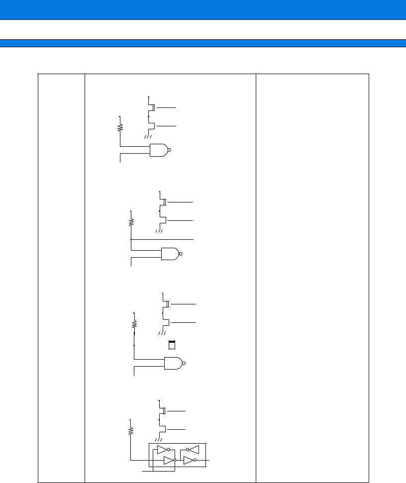
MB90230 Series
(Continued)
Type |
|
|
|
|
|
|
|
Circuit |
|
Remarks |
|
|
|
|
|
|
|
|
|
|
|
|
|
I |
|
|
|
|
|
|
|
|
• CMOS level output |
||
|
|
|
|
|
|
|
|
|
Open-drain control signal |
• |
Hysteresis input |
|
|
|
|
|
|
|
|
|
• |
Open-drain control provided |
|
|
|
|
|
|
|
|
|
|
|||
|
|
|
|
|
|
|
|
|
|
|
|
|
|
|
|
|
|
|
|
|
|
|
|
|
|
|
|
|
|
|
|
|
|
|
|
|
|
|
|
|
|
|
|
|
|
|
|
|
|
|
|
|
|
|
|
|
|
|
|
|
|
|
|
|
|
|
|
CMOS |
|
|
|
|
|
|
|
|
|
|
|
|
|
|
|
|
|
|
|
Standby control |
|||||||
|
|
|
|
|
|
|
|
|
J |
|
|
|
|
|
|
|
• CMOS level input/output |
|
|
|
|
|
|
|
|
• Analog input |
|
|
|
|
|
|
|
|
|
|
|
|
|
|
Analog input |
|
|
|
|
|
|
|
|
|
|
|
|
|
|
|
|
|
|
|
|
|
|
|
|
|
|
|
|
|
|
|
|
|
|
|
|
|
|
|
|
|
|
|
|
|
|
|
|
|
|
|
|
|
|
|
|
|
|
|
|
|
|
|
|
|
|
|
|
|
|
|
|
|
|
|
|
|
|
|
|
|
|
|
|
|
|
|
|
|
|
|
|
|
|
|
|
|
|
|
|
|
|
|
|
|
|
|
|
|
|
|
|
|
|
|
|
|
|
|
CMOS |
|
|
|
|
|
|
|
|
|
|
|
|
|
|
|
|
|
|
Standby control |
|||||||||||
|
|
|
|
|
|
|
|
|
|
|
|
|
|
|
K |
|
|
|
|
|
|
|
|
|
|
|
|
|
• CMOS level input/output |
|
|
|
|
|
|
|
|
|
|
|
|
|
|
• Analog output |
|
|
|
|
|
|
|
|
|
|
|
|
|
|
|
|
|
|
|
|
|
|
|
|
|
|
|
|
|
• Also serving for D/A output |
|
|
|
|
|
|
|
|
|
|
|
|
|
|
|
|
|
|
|
|
|
|
|
|
|
|
|
|
|
|
|
|
|
|
|
|
|
|
|
|
|
|
|
|
|
|
|
|
|
|
|
|
|
|
|
|
|
|
|
|
|
|
|
|
|
|
|
|
|
|
|
|
|
|
|
|
|
|
|
|
|
|
|
|
|
|
|
|
|
|
|
|
|
|
|
|
|
|
|
|
|
|
|
|
|
|
|
|
|
|
|
|
|
|
|
|
|
|
|
|
|
|
|
|
|
|
|
|
|
|
|
|
|
|
|
|
|
|
|
|
|
|
|
|
|
|
|
|
|
|
|
|
DA output |
|
|
|
|
|
|
|
|
|
|
|
|
|
|
|
|
|
|||
|
|
|
|
|
|
|
|
|
|
|
|
|
|
|
|
|
CMOS |
|
|
|
|
|
|
|
|
|
|
|
|
|
|
|
|
|
|
||
|
|
|
|
|
|
|
|
|
|
|
|
|
|
|
|
|
||
|
|
|
|
|
|
|
|
|
|
|
|
|
|
|
||||
|
|
Standby control |
||||||||||||||||
|
|
|
|
|
|
|
|
|
|
|
|
|
|
|
|
|
|
|
L |
|
|
|
|
|
|
|
|
|
|
|
|
|
|
|
|
• CMOS level output |
|
|
|
|
|
|
|
|
|
|
|
|
|
|
|
|||||
|
|
|
|
|
|
|
|
|
|
|
|
|
|
|
|
|
|
• Hysteresis input |
|
|
|
|
|
|
|
|
|
|
|
|
|
|
Open-drain control signal |
||||
|
|
|
|
|
|
|
|
|
|
|
|
|
|
|
|
|
|
• Open-drain control provided |
|
|
|
|
|
|
|
|
|
|
|
|
|
|
|
|
|||
|
|
|
|
|
|
|
|
|
|
|
|
|
|
|
|
|
|
|
|
|
|
|
|
|
|
|
|
|
|
|
|
|
|
|
|
|
|
|
|
|
|
|
|
|
|
|
|
|
|
|
|
|
|
|
|
|
|
|
|
|
|
|
|
|
|
|
|
|
|
|
|
|
|
|
|
|
|
|
|
|
|
|
|
|
|
|
|
|
|
|
|
|
|
|
|
|
|
|
|
|
|
|
|
|
|
|
|
|
|
|
|
|
|
Standby control
14
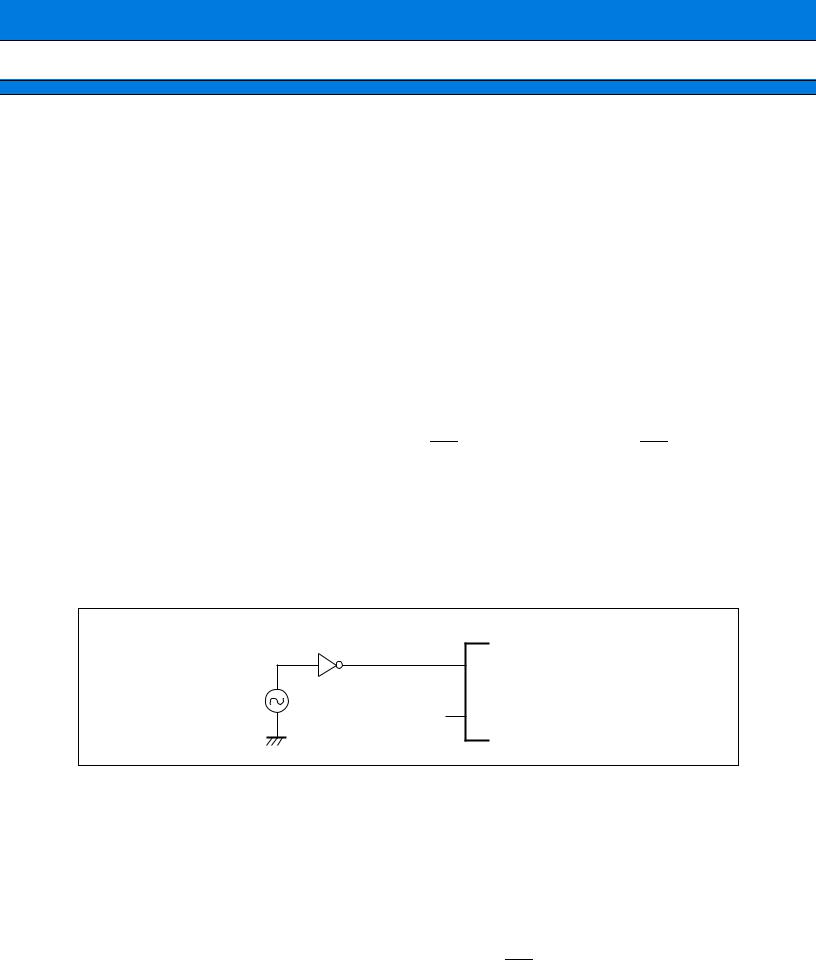
MB90230 Series
■ HANDLING DEVICES
1.Preventing Latchup
Latchup may occur on CMOS ICs if voltage higher than VCC or lower than VSS is applied to input and output pins other than mediumto high-voltage pins or if higher than the voltage wihich shows on “1. Absolute Maximum Ratings” in section “ ■ Electrical Characteristics” is applied between VCC and VSS.
When latchup occurs, power supply current increases rapidly and might thermally damage elements. When using, take great care not to exceed the absolute maximum ratings.
Also, take care to prevent the analog power supply (AVCC and AVR) and analog input from exceeding the digital power supply (VCC) when the analog system power supply is turned on and off.
2.Treatment of Unused Pins
Leaving unused input pins open could cause malfunctions. They should be connected to a pull-up or pull-down resistor.
3.External Reset Input
To reset the internal circuit by the Low-level input to the RST pin, the Low-level input to the RST pin must be maintained for at least five machine cycles. Pay attention to it if the chip uses external clock input.
4.VCC and VSS Pins
Apply equal potential to the VCC and VSS pins.
5.Notes on Using an External Clock
When using an external clock, drive the X0 pin as illustrated below:
Use of External Clock
X0 MB90234
X1
6.Power-on Sequence for A/D Converter Power Supplies and Analog Inputs
Be sure to turn on the digital power supply (VCC) before applying voltage to the A/D converter power supplies (AVCC, AVRH, and AVRL) and analog inputs (AN0 to AN15).
When turning power supplies off, turn off the A/D converter power supplies (AVCC, AVRH, and AVRL) and analog inputs (AN0 to AN15) first, then the digital power supply (AVCC).
When turning AVRH on or off, be careful not to let it exceed AVCC.
7.Pin set when turning on power supplies
When turning on power supplies, set the hardware standby input pin (HST) to “H”.
15

MB90230 Series
8.Program Mode
When shipped from Fujitsu, and after each erasure, all bits (96K × 8 bits) in the MB90W234 and MB90P234 are in the “1” state. Data is introduced by selectively programming “0’s” into the desired bit locations. Bits cannot be set to 1 electrically.
9.Erasure Procedure
Data written in the MB90W234 is erased (from 0 to 1) by exposing the chip to ultraviolet rays with a wavelength of 2,537Å through the translucent cover.
Recommended irradiation dosage for exposure is 10 Wsec/cm2. This amount is reached in 15 to 20 minutes
with a commercial ultraviolet lamp positioned 2 to 3 cm above the package (when the package surface illuminance is 1200 µW/cm2).
If the ultraviolet lamp has a filter, remove the filter before exposure. Attaching a mirrored plate to the lamp increases the illuminance by a factor of 1.4 to 1.8, thus shortening the required erasure time. If the translucent part of the package is stained with oil or adhesive, transmission of ultraviolet rays is degraded, resulting in a longer erasure time. In that case, clean the translucent part using alcohol (or other solvent not affecting the package).
The above recommended dosage is a value which takes the guard band into consideration and is a multiple of the time in which all bits can be evaluated to have been erased. Observe the recommended dosage for erasure; the purpose of the guard band is to ensure erasure in all temperature and supply voltage ranges. In addition, check the lifespan of the lamp and control the illuminance appropriately.
Data in the MB90W234 is erased by exposure to light with a wavelength of 4000Å or less.
Data in the device is also erased even by exposure to fluorescent lamp light or sunlight although the exposure results in a much lower erasure rate than exposure to 2537Å ultraviolet rays. Note that exposure to such lights for an extended period will therefore affect system reliability. If the chip is used where it is exposed to any light with a wavelength of 4000Å or less, cover the translucent part, for example, with a protective seal to prevent the chip from being exposed to the light.
Exposure to light with a wavelength of 4,000 to 5,000Å or more will not erase data in the device. If the light applied to the chip has a very high illuminance, however, the device may cause malfunction in the circuit for reasons of general semiconductor characteristics. Although the circuit will recover normal operation when exposure is stopped, the device requires proper countermeasures for use in a place exposed continuously to such light even though the wavelength is 4,000Å or more.
16

MB90230 Series
10. Recommended Screening Conditions
High-temperature aging is recommended for screening before packaging.
Program, verify
Aging
+150°C, 48 Hrs.
Data verification
Assembly
11. Write Yield
OTPROM products cannot be write-tested for all bits due to their nature. Therefore the write yield cannot always be guaranteed to be 100%.
17

MB90230 Series
■ BLOCK DIAGRAM
X0, X1 4 |
|
CPU |
|
|
|
RST |
Clock controller |
F2MC-16F |
|
|
|
HST |
|
|
|
|
|
|
|
|
Interrupt controller |
|
|
|
RAM |
|
|
|
|
|
ROM |
|
External interrupt |
|
INT0 |
|
|
4 |
to |
||
|
|
|
|
INT3 |
|
|
|
|
|
|
|
SIN0 |
|
|
|
|
|
SOT0 |
UART |
|
|
|
PWM0 |
SCK0 |
|
bus |
8-bit PWM |
|
|
|
|
to |
|||
|
|
|
|
||
|
|
-16 |
6 ch |
|
PWM5 |
CKOT |
Communication prescaler |
F2MC |
|
|
|
|
|
|
TRG |
||
|
|
|
8-bit PPG timer |
|
|
|
|
|
|
PPG |
|
|
|
|
|
|
|
SIN1, 2 |
Extended serial |
|
I/O timer |
|
IN0, 1 |
SOT1, 2 |
|
16-bit input capture × 4 |
|
||
I/O interface |
|
|
|||
SCK1, 2 |
|
|
IN2, 3 |
||
|
|
16-bit free run timer |
|
||
|
|
|
|
OUT0, 1 |
|
|
|
|
|
|
|
AVcc |
|
|
16-bit output compare × 6 |
|
OUT2, 3 |
|
|
|
|
OUT4, 5 |
|
AVRH, AVRL |
|
|
|
|
|
|
|
|
2 |
|
|
AVss |
10-bit A/D converter |
|
|
ECS, ESK |
|
ATG |
|
|
|
|
|
|
|
Serial E2PROM interface |
|
EDO |
|
AN0 to AN7 |
|
|
|
|
EDI |
DA0 |
D/A converter |
|
|
|
|
DA1 |
|
Level comparator |
|
CMP |
|
|
|
|
I/O ports (84 lines)
8 |
|
8 |
|
8 |
|
8 |
|
8 |
|
8 |
|
8 |
|
7 |
|
8 |
|
7 |
|
6 |
|
|
|
|
|
|
|
|
|
|
|
|
|
|
|
|
|
|
|
|
|
|
|
P00 |
P10 |
P20 |
P30 |
P40 |
P50 |
P60 |
P70 |
P80 |
P90 |
PA0 |
|||||||||||
to |
to |
to |
to |
to |
to |
to |
to |
to |
to |
to |
|||||||||||
P07 |
P17 |
P27 |
P37 |
P47 |
P57 |
P67 |
P76 |
P87 |
P96 |
PA5 |
|||||||||||
P00 to P27 (24 lines): Provided with input pull-up resistor setting registers
P94 to P96, PA0 to PA5 (9 lines): Provided with open-drain setting registers
18
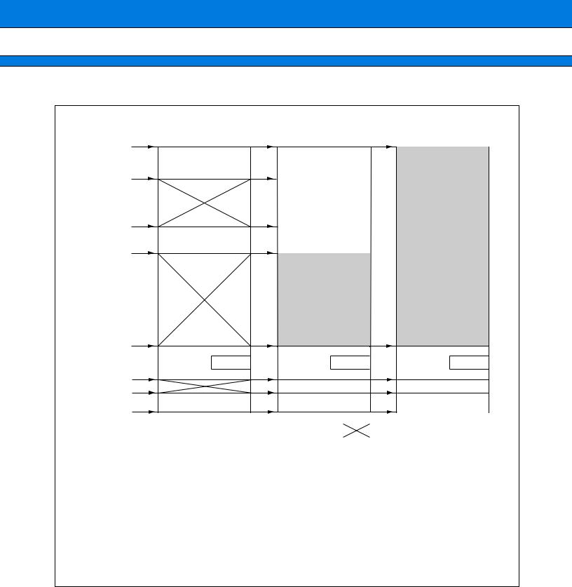
MB90230 Series
■ MEMORY MAP
|
Single-chip mode |
Internal ROM and |
|
External ROM and |
|
FFFFFFH |
external bus |
|
external bus |
||
|
|
|
|||
|
ROM area |
ROM area |
|
|
|
Address1# |
|
|
|
||
00FFFFH |
|
|
|
||
|
ROM area |
ROM area |
|
|
|
|
(FF bank image) |
(FF bank image) |
|
|
|
Address#2 |
|
|
|
||
|
|
|
|||
Address#3 |
|
|
|
|
|
|
|
|
|
|
|
|
|
|
|||
|
|
RAM |
Registers |
|
RAM |
Registers |
|
|
RAM |
Registers |
|
||||||
000100H |
|
|
|
|
|
|
|
|
|
|
|
|
|
|
|||
0000C0H |
|
|
|
|
|
|
|
|
|
|
|
|
|
|
|||
000000H |
Peripherals |
|
|
|
Peripherals |
|
|
Peripherals |
|
||||||||
|
|
|
|
|
|
|
|
|
|
|
|
|
|
|
|
||
|
|
|
|
|
Internal |
|
|
|
External |
|
Inhibited area |
|
|
||||
|
|
|
|
|
|
|
|
|
|
|
|||||||
|
|
|
|
|
|
|
|
|
|
|
|
|
|
|
|
|
|
|
Note: 000000H to 000005H and 000010H to 000015H are allocated for external use |
|
|||||||||||||||
|
when the external bus is enabled. |
|
|
|
|
|
|
|
|||||||||
|
|
|
|
|
|
|
|
|
|
|
|
|
|||||
|
Product type |
|
Address#1 |
|
|
|
|
Address#2 |
|
|
Address#3 |
|
|||||
|
MB90233 |
|
FF4000H |
|
|
|
|
004000H |
|
|
000900H |
|
|||||
|
MB90234 |
|
|
|
|
|
|
|
|
|
|
|
|
|
|
|
|
|
MB90P234 |
|
FE8000H |
|
|
|
|
004000H |
|
|
000D00H |
|
|||||
|
MB90W234 |
|
FE8000H |
|
|
|
|
004000H |
|
|
000D00H |
|
|||||
|
|
|
|
|
|
|
|
|
|
|
|
|
|||||
|
MB90V230 |
|
(FE0000H) |
|
|
|
|
(004000H) |
|
|
(001100H) |
|
|||||
The MB90230 series can access the 00 bank to read ROM data written to the upper 48-KB locations in the FF bank. An advantage of reading written to data addresses FFFFFFH-FF4000H from addresses 00FFFFH-004000H is that you can use the small model of a C compiler.
Note, however, that the products with more than 48KB ROM space (MB90V230, MB90P/W234, MB90234) cannot read data in addresses other than FFFFFFH to FF4000H from the 00 bank.
19

MB90230 Series
■ I/O MAP
Address |
Register |
Register |
Access |
Resouce |
Initial value |
|
name |
name |
|||||
|
|
|
|
|||
|
|
|
|
|
|
|
00H |
Port 0 data register |
PDR0 |
R/W |
Port 0 |
X X X X X X X X |
|
|
|
|
|
|
|
|
01H |
Port 1 data register |
PDR1 |
R/W |
Port 1 |
X X X X X X X X |
|
|
|
|
|
|
|
|
02H |
Port 2 data register |
PDR2 |
R/W |
Port 2 |
X X X X X X X X |
|
|
|
|
|
|
|
|
03H |
Port 3 data register |
PDR3 |
R/W |
Port 3 |
X X X X X X X X |
|
|
|
|
|
|
|
|
04H |
Port 4 data register |
PDR4 |
R/W |
Port 4 |
X X X X X X X X |
|
|
|
|
|
|
|
|
05H |
Port 5 data register |
PDR5 |
R/W |
Port 5 |
X X X X X X X X |
|
|
|
|
|
|
|
|
06H |
Port 6 data register |
PDR6 |
R/W |
Port 6 |
X X X X X X X X |
|
|
|
|
|
|
|
|
07H |
Port 7 data register |
PDR7 |
R/W |
Port 7 |
– X X X X X X X |
|
|
|
|
|
|
|
|
08H |
Port 8 data register |
PDR8 |
R/W |
Port 8 |
X X X X X X X X |
|
|
|
|
|
|
|
|
09H |
Port 9 data register |
PDR9 |
R/W |
Port 9 |
– X X X X X X X |
|
|
|
|
|
|
|
|
0AH |
Port A data register |
PDRA |
R/W |
Port A |
– – X X X X X X |
|
|
|
|
|
|
|
|
10H |
Port 0 direction register |
DDR0 |
R/W |
Port 0 |
0 0 0 0 0 0 0 0 |
|
|
|
|
|
|
|
|
11H |
Port 1 direction register |
DDR1 |
R/W |
Port 1 |
0 0 0 0 0 0 0 0 |
|
|
|
|
|
|
|
|
12H |
Port 2 direction register |
DDR2 |
R/W |
Port 2 |
0 0 0 0 0 0 0 0 |
|
|
|
|
|
|
|
|
13H |
Port 3 direction register |
DDR3 |
R/W |
Port 3 |
0 0 0 0 0 0 0 0 |
|
|
|
|
|
|
|
|
14H |
Port 4 direction register |
DDR4 |
R/W |
Port 4 |
0 0 0 0 0 0 0 0 |
|
|
|
|
|
|
|
|
15H |
Port 5 direction register |
DDR5 |
R/W |
Port 5 |
0 0 0 0 0 0 0 0 |
|
|
|
|
|
|
|
|
16H |
Port 6 direction register |
DDR6 |
R/W |
Port 6 |
0 0 0 0 0 0 0 0 |
|
|
|
|
|
|
|
|
17H |
Port 7 direction register |
DDR7 |
R/W |
Port 7 |
– 0 0 0 0 0 0 0 |
|
|
|
|
|
|
|
|
18H |
Port 8 direction register |
DDR8 |
R/W |
Port 8 |
0 0 0 0 0 0 0 0 |
|
|
|
|
|
|
|
|
19H |
Port 9 direction register |
DDR9 |
R/W |
Port 9 |
– 0 0 0 0 0 0 0 |
|
|
|
|
|
|
|
|
1AH |
Port A direction register |
DDRA |
R/W |
Port A |
– – 0 0 0 0 0 0 |
|
|
|
|
|
|
|
|
1BH |
Port 0 resistor register |
RDR0 |
R/W |
Port 0 |
0 0 0 0 0 0 0 0 |
|
|
|
|
|
|
|
|
1CH |
Port 1 resistor register |
RDR1 |
R/W |
Port 1 |
0 0 0 0 0 0 0 0 |
|
|
|
|
|
|
|
|
1DH |
Port 2 resistor register |
RDR2 |
R/W |
Port 2 |
0 0 0 0 0 0 0 0 |
|
|
|
|
|
|
|
|
1EH |
Port 9 pin register |
ODR9 |
R/W |
Port 9 |
– 0 0 0 – – – – |
|
|
|
|
|
|
|
|
1FH |
Port A pin register |
ODRA |
R/W |
Port A |
– – 0 0 0 0 0 0 |
|
|
|
|
|
|
|
|
20H |
Mode control register |
UMC |
R/W |
UART |
0 0 0 0 0 1 0 0 |
|
|
|
|
|
|
|
|
21H |
Status register |
USR |
R/W |
|
0 0 0 1 0 0 0 0 |
|
|
|
|
|
|
|
|
22H |
Serial input register |
UIDR |
R/W |
|
X X X X X X X X |
|
|
/Serial output register |
/UODR |
|
|
||
|
|
|
|
|||
|
|
|
|
|
|
|
23H |
Rate and data register |
URD |
R/W |
|
0 0 0 0 – – 0 0 |
|
|
|
|
|
|
|
|
24H |
Serial mode control status register |
SMCS |
R/W |
Extended serial |
– – – 0 0 0 0 0 |
|
|
|
|
|
I/O interface |
|
|
25H |
|
|
|
0 0 0 0 0 0 1 0 |
||
|
|
|
|
|
|
(Continued)
20
MB90230 Series
|
|
|
|
|
|
|
|
|
|
|
|
|
|
|
|
|
Address |
Register |
Register |
Access |
Resouce |
Initial value |
|
|
name |
name |
|
||||
|
|
|
|
|
|
||
|
|
|
|
|
|
|
|
|
26H |
Serial data register |
SDR |
R/W |
Extended serial |
X X X X X X X X |
|
|
|
|
|
|
I/O interface |
|
|
|
|
|
|
|
|
|
|
|
27H |
Reserved area |
— |
— |
— |
— |
|
|
|
|
|
|
|
|
|
|
28H |
Cycle setting register |
PCSR |
W |
8-bit |
X X X X X X X X |
|
|
|
|
|
|
PPG timer |
|
|
|
29H |
Duty factor setting register |
PDUT |
W |
X X X X X X X X |
|
|
|
|
|
|||||
|
|
|
|
|
|
|
|
|
2AH |
Control status register |
PCNTL |
R/W |
|
0 0 0 0 0 0 0 0 |
|
|
|
|
|
|
|
|
|
|
2BH |
|
PCNTH |
|
|
0 0 0 0 0 0 0 – |
|
|
|
|
|
|
|
|
|
|
2CH |
Reserved area |
— |
— |
— |
— |
|
|
|
|
|
|
|
|
|
|
2DH |
Communication prescaler |
CDCR |
R/W |
UART, CKOT, |
0 – – – 1 1 1 1 |
|
|
|
|
|
|
I/O, serial IF |
|
|
|
|
|
|
|
|
|
|
|
2EH |
Clock control register |
CLKR |
R/W |
CKOT output |
– – – – – 0 0 0 |
|
|
|
|
|
|
|
|
|
|
2FH |
Level comparator |
LVLC |
R/W |
Level |
X X X X 0 0 0 0 |
|
|
|
|
|
|
comparator |
|
|
|
|
|
|
|
|
|
|
|
30H |
Interrupt/DTP enable register |
ENIR |
R/W |
DTP/external |
– – – – 0 0 0 0 |
|
|
|
|
|
|
interrupt |
|
|
|
31H |
Interrupt/DTP factor register |
EIRR |
R/W |
– – – – 0 0 0 0 |
|
|
|
|
|
|||||
|
|
|
|
|
|
|
|
|
32H |
Request level setting register |
ELVR |
R/W |
|
0 0 0 0 0 0 0 0 |
|
|
|
|
|
|
|
|
|
|
33H |
Reserved area |
— |
— |
— |
— |
|
|
|
|
|
|
|
|
|
|
34H |
Analog input enable register |
ADER |
R/W |
10-bit A/D |
1 1 1 1 1 1 1 1 |
|
|
|
|
|
|
converter |
|
|
|
35H |
Reserved area |
— |
— |
— |
|
|
|
|
|
|||||
|
|
|
|
|
|
|
|
|
36H |
Control status data register |
ADCS0 |
R/W |
|
0 0 0 0 0 0 0 0 |
|
|
|
|
|
|
|
|
|
|
37H |
|
ADCS1 |
|
|
0 0 0 0 0 0 0 0 |
|
|
|
|
|
|
|
|
|
|
38H |
Data register |
ADCR0 |
R |
|
X X X X X X X X |
|
|
|
|
|
|
|
|
|
|
39H |
|
ADCR1 |
|
|
0 0 0 0 0 0 X X |
|
|
|
|
|
|
|
|
|
|
3AH |
Reserved area |
— |
— |
— |
— |
|
|
|
|
|
|
|
|
|
|
3BH |
Reserved area |
— |
— |
— |
— |
|
|
|
|
|
|
|
|
|
|
3CH |
D/A converter data register 0 |
DAT0 |
R/W |
8-bit D/A |
X X X X X X X X |
|
|
|
|
|
|
converter |
|
|
|
3DH |
D/A converter data register 1 |
DAT1 |
R/W |
0 0 0 0 0 0 0 0 |
|
|
|
|
|
|||||
|
|
|
|
|
|
|
|
|
3EH |
D/A control register |
DACR |
R/W |
|
– – – – – – 0 0 |
|
|
|
|
|
|
|
|
|
|
3FH |
Reserved area |
— |
— |
— |
— |
|
|
|
|
|
|
|
|
|
|
40H |
PWM data register 0 |
PWD0 |
R/W |
8-bit |
0 0 0 0 0 0 0 0 |
|
|
|
|
|
|
PWM0, 1 |
|
|
|
41H |
PWM data register 1 |
PWD1 |
R/W |
0 0 0 0 0 0 0 0 |
|
|
|
|
|
|||||
|
|
|
|
|
|
|
|
|
42H |
Control status data register 0, 1 |
PWC01 |
R/W |
|
0 0 0 0 0 0 0 0 |
|
|
|
|
|
|
|
|
|
|
43H |
Reserved area |
— |
— |
— |
— |
|
|
|
|
|
|
|
|
|
|
44H |
PWM data register 2 |
PWD2 |
R/W |
8-bit |
0 0 0 0 0 0 0 0 |
|
|
|
|
|
|
PWM2, 3 |
|
|
|
45H |
PWM data register 3 |
PWD3 |
R/W |
0 0 0 0 0 0 0 0 |
|
|
|
|
|
|||||
|
|
|
|
|
|
|
|
|
46H |
Control status register 2, 3 |
PWC23 |
R/W |
|
0 0 0 0 0 0 0 0 |
|
|
|
|
|
|
|
|
|
(Continued)
21

MB90230 Series
|
|
|
|
|
|
|
|
|
|
|
|
|
|
|
|
|
Address |
Register |
Register |
Access |
Resouce |
Initial value |
|
|
name |
name |
|
||||
|
|
|
|
|
|
||
|
|
|
|
|
|
|
|
|
47H |
Reserved area |
— |
— |
— |
— |
|
|
|
|
|
|
|
|
|
|
48H |
PWM data register 4 |
PWD4 |
R/W |
8-bit |
0 0 0 0 0 0 0 0 |
|
|
|
|
|
|
PWM4, 5 |
|
|
|
49H |
PWM data register 5 |
PWD5 |
R/W |
0 0 0 0 0 0 0 0 |
|
|
|
|
|
|||||
|
|
|
|
|
|
|
|
|
4AH |
Control status register 4, 5 |
PWC45 |
R/W |
|
0 0 0 0 0 0 0 0 |
|
|
|
|
|
|
|
|
|
|
4BH |
Reserved area |
— |
— |
— |
— |
|
|
|
|
|
|
|
|
|
|
4CH |
Data register |
TCDT |
R |
16-bit free |
0 0 0 0 0 0 0 0 |
|
|
|
|
|
|
run timer |
|
|
|
4DH |
|
|
|
0 0 0 0 0 0 0 0 |
|
|
|
|
|
|
|
|
||
|
|
|
|
|
|
|
|
|
4EH |
Control status register |
TCCS |
R/W |
|
0 0 0 0 0 0 0 0 |
|
|
|
|
|
|
|
|
|
|
4FH |
Reserved area |
— |
— |
— |
— |
|
|
|
|
|
|
|
|
|
|
50H |
Compare register 0 |
OCP0 |
R/W |
Output |
X X X X X X X X |
|
|
|
|
|
|
compare 0, 1 |
|
|
|
51H |
|
|
|
X X X X X X X X |
|
|
|
|
|
|
|
|
||
|
|
|
|
|
|
|
|
|
52H |
Compare register 1 |
OCP1 |
R/W |
|
X X X X X X X X |
|
|
|
|
|
|
|
|
|
|
53H |
|
|
|
|
X X X X X X X X |
|
|
|
|
|
|
|
|
|
|
54H |
Control status register 0, 1 |
CS00 |
R/W |
|
0 0 0 0 – – 0 0 |
|
|
|
|
|
|
|
|
|
|
55H |
|
CS01 |
|
|
– – – 0 0 0 0 0 |
|
|
|
|
|
|
|
|
|
|
56H |
Reserved area |
— |
— |
— |
— |
|
|
|
|
|
|
|
|
|
|
57H |
Reserved area |
— |
— |
— |
— |
|
|
|
|
|
|
|
|
|
|
58H |
Compare register 2 |
OCP2 |
R/W |
Output |
X X X X X X X X |
|
|
|
|
|
|
compare 2, 3 |
|
|
|
59H |
|
|
|
X X X X X X X X |
|
|
|
|
|
|
|
|
||
|
|
|
|
|
|
|
|
|
5AH |
Compare register 3 |
OCP3 |
R/W |
|
X X X X X X X X |
|
|
|
|
|
|
|
|
|
|
5BH |
|
|
|
|
X X X X X X X X |
|
|
|
|
|
|
|
|
|
|
5CH |
Control status register 2, 3 |
CS10 |
R/W |
|
0 0 0 0 – – 0 0 |
|
|
|
|
|
|
|
|
|
|
5DH |
|
CS11 |
|
|
– – – 0 0 0 0 0 |
|
|
|
|
|
|
|
|
|
|
5EH |
Reserved area |
— |
— |
— |
— |
|
|
|
|
|
|
|
|
|
|
5FH |
Reserved area |
— |
— |
— |
— |
|
|
|
|
|
|
|
|
|
|
60H |
Compare register 4 |
OCP4 |
R/W |
Output |
X X X X X X X X |
|
|
|
|
|
|
compare 4, 5 |
|
|
|
61H |
|
|
|
X X X X X X X X |
|
|
|
|
|
|
|
|
||
|
|
|
|
|
|
|
|
|
62H |
Compare register 5 |
OCP5 |
R/W |
|
X X X X X X X X |
|
|
|
|
|
|
|
|
|
|
63H |
|
|
|
X X X X X X X X |
|
|
|
|
|
|
|
|
||
|
|
|
|
|
|
|
|
|
64H |
Control status register 4, 5 |
CS20 |
R/W |
|
0 0 0 0 – – 0 0 |
|
|
|
|
|
|
|
||
|
65H |
CS21 |
|
– – – 0 0 0 0 0 |
|
||
|
|
|
|
|
|||
|
|
|
|
|
|
|
|
|
66H |
Reserved area |
— |
— |
— |
— |
|
|
|
|
|
|
|
|
|
|
67H to |
Reserved area |
— |
— |
— |
— |
|
|
6FH |
|
|
||||
|
|
|
|
|
|
|
|
|
|
|
|
|
|
|
|
|
|
|
|
|
|
(Continued) |
|
22

MB90230 Series
|
|
|
|
|
|
|
|
|
|
|
|
|
|
|
|
|
Address |
Register |
Register |
Access |
Resouce |
Initial value |
|
|
name |
name |
|
||||
|
|
|
|
|
|
||
|
|
|
|
|
|
|
|
|
70H |
Capture register 0 |
ICP0 |
R/W |
Input capture 0, |
X X X X X X X X |
|
|
|
|
|
|
1 |
|
|
|
71H |
|
|
|
X X X X X X X X |
|
|
|
|
|
|
|
|
||
|
|
|
|
|
|
|
|
|
72H |
Capture register 1 |
ICP1 |
R/W |
|
X X X X X X X X |
|
|
|
|
|
|
|
|
|
|
73H |
|
|
|
|
X X X X X X X X |
|
|
|
|
|
|
|
|
|
|
74H |
Control status register 0, 1 |
ICS0 |
R/W |
|
0 0 0 0 0 0 0 0 |
|
|
|
|
|
|
|
|
|
|
75H to |
Reserved area |
— |
— |
— |
— |
|
|
77H |
|
|
|
|
|
|
|
|
|
|
|
|
|
|
|
78H |
Capture register 2 |
ICP2 |
R/W |
Input capture 2, |
X X X X X X X X |
|
|
|
|
|
|
3 |
|
|
|
79H |
|
|
|
X X X X X X X X |
|
|
|
|
|
|
|
|
||
|
|
|
|
|
|
|
|
|
7AH |
Capture register 3 |
ICP3 |
R/W |
|
X X X X X X X X |
|
|
|
|
|
|
|
|
|
|
7BH |
|
|
|
|
X X X X X X X X |
|
|
|
|
|
|
|
|
|
|
7CH |
Control status register 2, 3 |
ICS1 |
R/W |
|
0 0 0 0 0 0 0 0 |
|
|
|
|
|
|
|
|
|
|
7DH to |
Reserved area |
— |
— |
— |
— |
|
|
7FH |
|
|
|
|
|
|
|
|
|
|
|
|
|
|
|
80H |
OP code register |
EOPC |
R/W |
Serial E2PROM |
– – – – 0 0 0 0 |
|
|
|
|
|
|
interface |
|
|
|
81H |
Format status register |
ECTS |
R/W |
0 0 0 0 0 0 0 0 |
|
|
|
|
|
|||||
|
|
|
|
|
|
|
|
|
82H |
Data register |
EDAT |
R/W |
|
X X X X X X X X |
|
|
|
|
|
|
|
|
|
|
83H |
|
|
|
|
X X X X X X X X |
|
|
|
|
|
|
|
|
|
|
84H |
Address register |
EADR |
R/W |
|
0 0 0 0 0 0 0 0 |
|
|
|
|
|
|
|
|
|
|
85H |
|
|
|
|
0 0 – – – 0 0 0 |
|
|
|
|
|
|
|
|
|
|
86H to |
Reserved area |
— |
— |
— |
— |
|
|
8FH |
|
|
|
|
|
|
|
|
|
|
|
|
|
|
|
90H to |
System reserved area |
— |
*1 |
— |
— |
|
|
9EH |
|
|
|
|
|
|
|
|
|
|
|
|
|
|
|
9FH |
Delayed interrupt source generate/ |
DIRR |
R/W |
Delayed interrupt |
– – – – – – – 0 |
|
|
|
release register |
|
|
generation module |
|
|
|
|
|
|
|
|
|
|
|
A0H |
Standby control register |
STBYC |
R/W |
Low-power |
0 0 0 1 X X X X |
|
|
|
|
|
|
consumption |
|
|
|
|
|
|
|
mode |
|
|
|
|
|
|
|
|
|
|
|
A1H |
Reserved area |
— |
— |
— |
— |
|
|
|
|
|
|
|
|
|
|
A2H |
Reserved area |
— |
— |
— |
— |
|
|
|
|
|
|
|
|
|
|
A3H |
Middle address control register |
MACR |
W |
External pin |
*2 |
|
|
|
|
|
|
|
|
|
|
A4H |
Upper address control register |
HACR |
W |
External pin |
*2 |
|
|
|
|
|
|
|
|
|
|
A5H |
External pin control register |
EPCR |
W |
External pin |
*2 |
|
|
|
|
|
|
|
|
|
|
A6H |
Reserved area |
— |
— |
— |
— |
|
|
|
|
|
|
|
|
|
|
A7H |
Reserved area |
— |
— |
— |
— |
|
|
|
|
|
|
|
|
|
|
A8H |
Watchdog timer control register |
TWC |
R/W |
Watchdog timer/ |
X X X X X X X X |
|
|
|
|
|
|
reset |
|
|
|
|
|
|
|
|
|
|
|
|
|
|
|
|
(Continued) |
|
23

MB90230 Series
|
|
|
|
|
|
|
|
|
|
|
|
|
|
|
|
|
Address |
Register |
Register |
Access |
Resouce |
Initial value |
|
|
name |
name |
|
||||
|
|
|
|
|
|
||
|
|
|
|
|
|
|
|
|
A9H |
Timebase timer control register |
TBTC |
R/W |
Timebase |
– – – 0 0 0 0 0 |
|
|
|
|
|
|
timer |
|
|
|
|
|
|
|
|
|
|
|
AAH to |
Reserved area |
— |
— |
— |
— |
|
|
AFH |
|
|
|
|
|
|
|
|
|
|
|
|
|
|
|
B0H |
Interrupt control register 00 |
ICR00 |
R/W |
Interrupt |
0 0 0 0 0 1 1 1 |
|
|
|
|
|
|
controller |
|
|
|
B1H |
Interrupt control register 01 |
ICR01 |
R/W |
0 0 0 0 0 1 1 1 |
|
|
|
|
|
|||||
|
|
|
|
|
|
|
|
|
B2H |
Interrupt control register 02 |
ICR02 |
R/W |
|
0 0 0 0 0 1 1 1 |
|
|
|
|
|
|
|
|
|
|
B3H |
Interrupt control register 03 |
ICR03 |
R/W |
|
0 0 0 0 0 1 1 1 |
|
|
|
|
|
|
|
|
|
|
B4H |
Interrupt control register 04 |
ICR04 |
R/W |
|
0 0 0 0 0 1 1 1 |
|
|
|
|
|
|
|
|
|
|
B5H |
Interrupt control register 05 |
ICR05 |
R/W |
|
0 0 0 0 0 1 1 1 |
|
|
|
|
|
|
|
|
|
|
B6H |
Interrupt control register 06 |
ICR06 |
R/W |
|
0 0 0 0 0 1 1 1 |
|
|
|
|
|
|
|
|
|
|
B7H |
Interrupt control register 07 |
ICR07 |
R/W |
|
0 0 0 0 0 1 1 1 |
|
|
|
|
|
|
|
|
|
|
B8H |
Interrupt control register 08 |
ICR08 |
R/W |
|
0 0 0 0 0 1 1 1 |
|
|
|
|
|
|
|
|
|
|
B9H |
Interrupt control register 09 |
ICR09 |
R/W |
|
0 0 0 0 0 1 1 1 |
|
|
|
|
|
|
|
|
|
|
BAH |
Interrupt control register 10 |
ICR10 |
R/W |
|
0 0 0 0 0 1 1 1 |
|
|
|
|
|
|
|
|
|
|
BBH |
Interrupt control register 11 |
ICR11 |
R/W |
|
0 0 0 0 0 1 1 1 |
|
|
|
|
|
|
|
|
|
|
BCH |
Interrupt control register 12 |
ICR12 |
R/W |
|
0 0 0 0 0 1 1 1 |
|
|
|
|
|
|
|
|
|
|
BDH |
Interrupt control register 13 |
ICR13 |
R/W |
|
0 0 0 0 0 1 1 1 |
|
|
|
|
|
|
|
|
|
|
BEH |
Interrupt control register 14 |
ICR14 |
R/W |
|
0 0 0 0 0 1 1 1 |
|
|
|
|
|
|
|
|
|
|
BFH |
Interrupt control register 15 |
ICR15 |
R/W |
|
0 0 0 0 0 1 1 1 |
|
|
|
|
|
|
|
|
|
|
C0H to |
External area |
— |
— |
— |
*3 |
|
|
FFH |
|
|
|
|
|
|
|
|
|
|
|
|
|
|
Initial values
0:The initial value for the bit is “0.”
1:The initial value for the bit is “1.”
X: The initial value for the bit is undefined.
–: The bit is not used; the initial value is undefined. *1: Access inhibited
*2: The initial value depends on each bus mode.
*3: Only this area can be used as the external access area in the area that follows address 0000FFH. Access to any address in reserved areas specified in the I/O map table is handled as access to an internal area. An access signal to the external bus is not generated.
24

MB90230 Series
■INTERRUPT VECTORS AND INTERRUPT CONTROL REGISTERS FOR INTERRUPT SOURCES
|
I2OS |
Interrupt vector |
Interrupt control |
||||
Interrupt source |
register |
||||||
support |
|
|
|
|
|
|
|
|
No. |
|
Address |
ICR |
Address |
||
|
|
|
|||||
|
|
|
|
|
|
|
|
Reset |
× |
#08 |
|
08H |
FFFFDCH |
— |
— |
|
|
|
|
|
|
|
|
INT9 instruction |
× |
#09 |
|
09H |
FFFFD8H |
— |
— |
|
|
|
|
|
|
|
|
Exceptional |
× |
#10 |
|
0AH |
FFFFD4H |
— |
— |
|
|
|
|
|
|
|
|
External interrupt (INT0) 0 ch |
|
#11 |
|
0BH |
FFFFD0H |
ICR00 |
0000B0H |
|
|
|
|
|
|
|
|
External interrupt (INT1) 1 ch |
|
#12 |
|
0CH |
FFFFCCH |
|
|
|
|
|
|
|
|
|
|
External interrupt (INT2) 2 ch |
|
#13 |
|
0DH |
FFFFC8H |
ICR01 |
0000B1H |
|
|
|
|
|
|
|
|
External interrupt (INT3) 3 ch |
|
#14 |
|
0EH |
FFFFC4H |
|
|
|
|
|
|
|
|
|
|
Extended serial I/O interface |
|
#15 |
|
0FH |
FFFFC0H |
ICR02 |
0000B2H |
|
|
|
|
|
|
|
|
Serial E2PROM interface |
|
#17 |
|
11H |
FFFFB8H |
ICR03 |
0000B3H |
|
|
|
|
|
|
|
|
Input capture channel 0 |
|
#19 |
|
13H |
FFFFB0H |
ICR04 |
0000B4H |
|
|
|
|
|
|
|
|
Input capture channel 1 |
|
#21 |
|
15H |
FFFFA8H |
ICR05 |
0000B5H |
|
|
|
|
|
|
|
|
Input capture channel 2 |
|
#23 |
|
17H |
FFFFA0H |
ICR06 |
0000B6H |
|
|
|
|
|
|
|
|
Input capture channel 3 |
|
#24 |
|
18H |
FFFF9CH |
|
|
|
|
|
|
|
|
|
|
Output compare channel 0 |
|
#25 |
|
19H |
FFFF98H |
ICR07 |
0000B7H |
|
|
|
|
|
|
|
|
Output compare channel 1 |
|
#26 |
|
1AH |
FFFF94H |
|
|
|
|
|
|
|
|
|
|
Output compare channel 2 |
|
#27 |
|
1BH |
FFFF90H |
ICR08 |
0000B8H |
|
|
|
|
|
|
|
|
Output compare channel 3 |
|
#28 |
|
1CH |
FFFF8CH |
|
|
|
|
|
|
|
|
|
|
Output compare channel 4 |
|
#29 |
|
1DH |
FFFF88H |
ICR09 |
0000B9H |
|
|
|
|
|
|
|
|
Output compare channel 5 |
|
#30 |
|
1EH |
FFFF84H |
|
|
|
|
|
|
|
|
|
|
16-bit free run timer overflow |
|
#31 |
|
1FH |
FFFF80H |
ICR10 |
0000BAH |
|
|
|
|
|
|
|
|
Timebase timer overflow |
|
#32 |
|
20H |
FFFF7CH |
|
|
|
|
|
|
|
|
|
|
8-bit PPG timer |
|
#33 |
|
21H |
FFFF78H |
ICR11 |
0000BBH |
|
|
|
|
|
|
|
|
Level comparator |
|
#34 |
|
22H |
FFFF74H |
|
|
|
|
|
|
|
|
|
|
UART reception |
|
#35 |
|
23H |
FFFF70H |
ICR12 |
0000BCH |
|
|
|
|
|
|
|
|
UART transmission |
|
#37 |
|
25H |
FFFF68H |
ICR13 |
0000BDH |
|
|
|
|
|
|
|
|
End of A/D conversion |
|
#39 |
|
27H |
FFFF60H |
ICR14 |
0000BEH |
|
|
|
|
|
|
|
|
Delayed interrupt |
× |
#42 |
|
2AH |
FFFF54H |
ICR15 |
0000BFH |
|
|
|
|
|
|
|
|
Stack fault |
× |
#256 |
|
FFH |
FFFC00H |
— |
— |
|
|
|
|
|
|
|
|
 : The request flag is cleared by the EI2OS interrupt clear signal.
 : The request flag is cleared by the EI2OS interrupt clear signal. The stop request is available.
 : The request flag is not cleared by the EI2OS interrupt clear signal.
25

MB90230 Series
■ PERIPHERAL RESOURCES
1.I/O Ports
Each pin in each port can be specified for input or output by setting the direction register when the corresponding peripheral resource is not set to use that pin. When the data register is read, the value depending on the pin level is read whenever the pin serves for input. When the data register is read with the pin serving for output, the latch value of the data register is read. This also applies to read operation by the read modify write instruction.
•General-purpose I/O port
Internal data bus
Data register read
Data register
Data register write
Direction register
Direction register write
Direction register read
Pin
• Port with pull-up resistor setting register
|
|
Pull-up resistor (Approx. 50 kΩ) |
|
Data register |
Port input/output |
data bus |
|
|
Internal |
Direction register read |
|
|
|
|
|
Resistor register |
|
26
 Loading...