


|
|
|
|
|
|
FUJITSU SEMICONDUCTOR |
|
DS05-20890-1E |
|
|
DATA SHEET |
|
|
|
|
|
|
|
|
|
|
|
|
|
|
|
|
|
|
|
|
|
|
|
PAGE MODE FLASH MEMORY
CMOS
32 M (2 M × 16/1 M × 32) BIT
MBM29PL3200TE/BE 70/90
■ DESCRIPTION
The MBM29PL3200TE/BE is 32 M-bit, 3.0 V-only Page mode Flash memory organized as 2 M words of 16 bits each or 1 M words of 32 bits each. The device is offered in 90-pin SSOP and 84-ball FBGA packages. This device is designed to be programmed in-system with the standard system 3.0 V VCC supply. 12.0 V VPP and 5.0 V VCC are not required for write or erase operations. The device can also be reprogrammed in standard EPROM programmers.
(Continued)
■ PRODUCT LINE-UP
|
Part No. |
|
MBM29PL3200TE/BE |
|
|
+0.3 V |
70 |
|
|
Ordering Part No. |
VCC = 3.3 V −0.3 V |
|||
+0.6 V |
|
90 |
||
|
||||
|
VCC = 3.0 V−0.3 V |
|||
Max. Random Address Access Time (ns) |
70 |
90 |
||
Max. Page Address Access Time (ns) |
25 |
35 |
||
Max. CE Access Time (ns) |
70 |
90 |
||
Max. OE Access Time (ns) |
25 |
35 |
||
■ PACKAGES
90-pin plastic SSOP |
84-ball plastic FBGA |
(FPT-90P-M01) |
(BGA-84P-M01) |

MBM29PL3200TE/BE70/90
(Continued)
The device provides truly high performance non-volatile Flash memory solution. The device offers fast page access times of 25 ns and 35 ns with random access times of 70 ns and 90 ns, allowing operation of high-speed microprocessors without wait states. To eliminate bus contention, the device has separate chip enable (CE), write enable (WE) and output enable (OE) controls. The page size is 8 words or 4 double words.
The device is command set compatible with JEDEC standard E2PROMs. Commands are written to the command register using standard microprocessor write timings. Register contents serve as input to an internal statemachine which controls the erase and programming circuitry. Write cycles also internally latch addresses and data needed for the programming and erase operations. Reading data out of the device is similar to reading from 5.0 V and 12.0 V Flash or EPROM devices.
The device is programmed by executing the program command sequence. This will invoke the Embedded ProgramTM * Algorithm, which is an internal algorithm that automatically times the program pulse widths and verifies proper cell margins. Typically, each sector can be programmed and verified in about 2.2 seconds. Erase is accomplished by executing the erase command sequence. This will invoke the Embedded EraseTM * Algorithm, which is an internal algorithm that automatically preprograms the array if it is not already programmed before executing the erase operation. During erase, the device automatically times the erase pulse widths and verifies proper cell margins.
Any individual sector is typically erased and verified in 4.8 second. (If already preprogrammed.)
The device also features a sector erase architecture. The sector mode allows each sector to be erased and reprogrammed without affecting other sectors. The device is erased when shipped from the factory.
The device features single 3.0 V power supply operation for both read and write functions. Internally generated and regulated voltages are provided for the program and erase operations. A low VCC detector automatically inhibits write operations on the loss of power. The end of program or erase is detected by Data Polling of DQ7, by the Toggle Bit feature on DQ6, output pin. Once the end of a program or erase cycle has been completed, the device internally resets to the read mode.
Fujitsu’s Flash technology combines years of Flash memory manufacturing experience to produce the highest levels of quality, reliability, and cost effectiveness. The device memory electrically erases all bits within a sector simultaneously via Fowler-Nordhiem tunneling. The words/double words are programmed one word/double word at a time using the EPROM programming mechanism of hot electron injection.
*: Embedded EraseTM and Embedded ProgramTM are trademarks of Advanced Micro Devices, Inc.
■FEATURES
•0.23 µm Process Technology
•Single 3.0 V read, program and erase
Minimized system level power requirements
•High Performance Page Mode
25 ns maximum page access time (70 ns random access time)
•8 words Page ( × 16) /4 double words ( × 32) size
•Compatible with JEDEC-standard commands
Uses same software commands as E2PROMs
•Compatible with JEDEC-standard world-wide pinouts
90-pin SSOP (Package suffix : PFV)
84-ball FBGA (Package suffix : PBT)
•Minimum 100,000 program/erase cycles
•Sector erase architecture
One 16 K word, two 8 K words, one 96 K word, and fifteen 128 K words sectors in word mode ( × 16)
One 8 K double word, two 4 K double words, one 48 K double word, and fifteen 64 K double words sectors in double word mode ( × 32)
Any combination of sectors can be concurrently erased. Also supports full chip erase
2

MBM29PL3200TE/BE70/90
•Boot Code Sector Architecture
T = Top sector
B = Bottom sector
•Embedded EraseTM Algorithms
Automatically pre-programs and erases the chip or any sector
•Embedded ProgramTM Algorithms
Automatically programs and verifies data at specified address
•Data Polling and Toggle Bit feature for detection of program or erase cycle completion
•Automatic sleep mode
When addresses remain stable, automatically switches themselves to low power mode
•Low VCC write inhibit ≤ 2.5 V
•Erase Suspend/Resume
Suspends the erase operation to allow a read data and/or program in another sector within the same device
•Sector protection
Hardware method disables any combination of sectors from program or erase operations
•Fast Programming Function by Extended command
•Temporary sector unprotection
Temporary sector unprotection with the software command
•In accordance with CFI (Common Flash Memory Interface)
3
MBM29PL3200TE/BE70/90
■ PIN ASSIGNMENTS
SSOP
(TOP VIEW)
N.C. |
1 |
90 |
N.C. |
||
N.C. |
2 |
89 |
N.C. |
||
N.C. |
3 |
88 |
ACC |
||
N.C. |
4 |
87 |
WP |
||
N.C. |
5 |
86 |
WE |
||
A0 |
6 |
85 |
N.C. |
||
A1 |
7 |
84 |
N.C. |
||
A2 |
8 |
83 |
N.C. |
|
|
A3 |
9 |
82 |
DW/W |
|
|
A4 |
10 |
81 |
OE |
||
A5 |
11 |
80 |
CE |
||
VCC |
12 |
79 |
VSS |
||
DQ0 |
13 |
78 |
DQ31/A-1 |
||
DQ16 |
14 |
77 |
DQ15 |
||
DQ1 |
15 |
76 |
DQ30 |
||
DQ17 |
16 |
75 |
DQ14 |
||
VSS |
17 |
74 |
VSS |
||
VCC |
18 |
73 |
VCC |
||
DQ2 |
19 |
72 |
DQ29 |
||
DQ18 |
20 |
71 |
DQ13 |
||
DQ3 |
21 |
70 |
DQ28 |
||
DQ19 |
22 |
69 |
DQ12 |
||
DQ4 |
23 |
68 |
DQ27 |
||
DQ20 |
24 |
67 |
DQ11 |
||
DQ5 |
25 |
66 |
DQ26 |
||
DQ21 |
26 |
65 |
DQ10 |
||
VSS |
27 |
64 |
VSS |
||
VCC |
28 |
63 |
VCC |
||
DQ6 |
29 |
62 |
DQ25 |
||
DQ22 |
30 |
61 |
DQ9 |
||
DQ7 |
31 |
60 |
DQ24 |
||
DQ23 |
32 |
59 |
DQ8 |
||
VSS |
33 |
58 |
VCC |
||
A6 |
34 |
57 |
A19 |
||
A7 |
35 |
56 |
A18 |
||
A8 |
36 |
55 |
A17 |
||
A9 |
37 |
54 |
A16 |
||
A10 |
38 |
53 |
A15 |
||
A11 |
39 |
52 |
A14 |
||
A12 |
40 |
51 |
A13 |
||
N.C. |
41 |
50 |
N.C. |
||
N.C. |
42 |
49 |
N.C. |
||
N.C. |
43 |
48 |
N.C. |
||
N.C. |
44 |
47 |
N.C. |
||
N.C. |
45 |
46 |
N.C. |
||
FPT-90P-M01
(Continued)
4

MBM29PL3200TE/BE70/90
(Continued)
FBGA
(TOP VIEW) Marking Side
|
B9 |
C9 |
D9 |
E9 |
F9 |
G9 |
H9 |
J9 |
|
|
DQ30 |
VCC |
DQ13 |
DQ12 |
DQ27 |
DQ26 |
VCC |
DQ9 |
|
A8 |
B8 |
C8 |
D8 |
E8 |
F8 |
G8 |
H8 |
J8 |
K8 |
CE |
VSS |
DQ15 |
DQ29 |
DQ28 |
DQ11 |
VSS |
DQ24 |
VCC |
A19 |
A7 |
B7 |
C7 |
D7 |
E7 |
F7 |
G7 |
H7 |
J7 |
K7 |
N.C. |
DW/W |
OE |
DQ14 |
VSS |
DQ10 |
DQ25 |
A18 |
A17 |
A16 |
A6 |
B6 |
C6 |
D6 |
E6 |
F6 |
G6 |
H6 |
J6 |
K6 |
WE |
N.C. |
N.C. |
DQ31/A-1 N.C. |
N.C. |
DQ8 |
A15 |
A14 |
A13 |
|
A5 |
B5 |
C5 |
D5 |
E5 |
F5 |
G5 |
H5 |
J5 |
K5 |
N.C. |
ACC |
WP |
N.C. |
N.C. |
N.C. |
N.C. |
N.C. |
N.C. |
N.C. |
A4 |
B4 |
C4 |
D4 |
E4 |
F4 |
G4 |
H4 |
J4 |
K4 |
A1 |
A2 |
A3 |
A0 |
DQ2 |
N.C. |
A12 |
A11 |
A9 |
A10 |
A3 |
B3 |
C3 |
D3 |
E3 |
F3 |
G3 |
H3 |
J3 |
K3 |
A4 |
A5 |
DQ0 |
DQ16 |
DQ18 |
DQ5 |
DQ21 |
A8 |
A6 |
A7 |
|
B2 |
C2 |
D2 |
E2 |
F2 |
G2 |
H2 |
J2 |
K2 |
|
VCC |
DQ1 |
VSS |
DQ19 |
DQ4 |
DQ6 |
DQ7 |
DQ23 |
VSS |
|
|
C1 |
D1 |
E1 |
F1 |
G1 |
H1 |
J1 |
|
|
|
DQ17 |
VCC |
DQ3 |
DQ20 |
VSS |
VCC |
DQ22 |
|
BGA-84P-M01
5

MBM29PL3200TE/BE70/90
■ PIN DESCRIPTIONS
|
|
|
|
|
|
|
|
Table 1 MBM29PL3200TE/BE Pin Configuration |
Pin Name |
Function |
|||||||
|
|
|||||||
A19 to A0, A-1 |
Address Input |
|||||||
|
|
|||||||
DQ31 to DQ0 |
Data Input/Output |
|||||||
|
|
|
|
|
|
|
|
|
|
|
|
|
|
|
|
|
Chip Enable |
|
|
CE |
||||||
|
|
|
|
|
|
|
||
|
|
|
|
|
|
|
|
Output Enable |
|
OE |
|||||||
|
|
|
|
|
|
|||
|
|
|
|
|
|
|
|
Write Enable |
|
WE |
|||||||
|
|
|
||||||
|
|
|
|
|
|
|
|
Selects 32-bit or 16-bit mode |
DW/W |
||||||||
|
|
|
|
|||||
|
|
|
|
|
|
|
Hardware Write Protection |
|
|
WP |
|||||||
|
|
|||||||
ACC |
Program Acceleration |
|||||||
|
|
|||||||
N.C. |
Pin Not Connected Internally |
|||||||
|
|
|
||||||
|
VSS |
Device Ground |
||||||
|
|
|
||||||
|
VCC |
Device Power Supply |
||||||
|
|
|
|
|
|
|
|
|
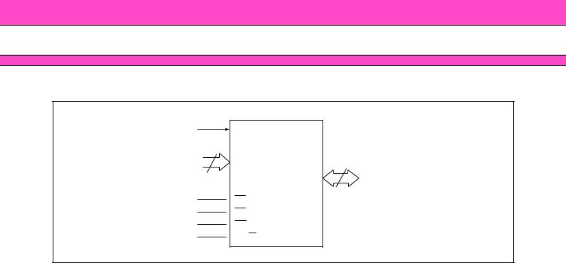
■ BLOCK DIAGRAM
VCC |
|
|
|
|
|
DQ31 to DQ0 |
|
|
|
|
|
|
|
VSS |
|
|
|
|
|
|
|
|
Erase Voltage |
|
|
Input/Output |
|
|
|
|
Generator |
|
|
Buffers |
WE |
State |
|
|
|
|
|
DW/W |
|
|
|
|
|
|
Control |
|
|
|
|
|
|
WP |
Circuit |
|
|
|
|
|
|
|
|
|
|
|
|
ACC |
(Command |
|
|
|
|
|
|
Register) |
Program Voltage |
|
|
|
|
|
|
|
|
|
|
|
|
|
Generator |
Chip Enable |
STB |
Data Latch |
|
|
|
|
Output Enable |
|
||
|
|
|
|
|
||
CE |
|
|
|
Logic |
|
|
OE |
|
|
|
|
|
|
|
|
|
STB |
Y-Decoder |
|
Y-Gating |
|
|
|
|
|
|
|
|
Low VCC Detector |
Timer for |
Address |
|
|
|
|
Program/Erase |
|
|
|||
|
|
|
Latch |
X-Decoder |
|
33,554,432 |
|
|
|
|
|
|
Cell Matrix |
A19 to A29 |
|
|
|
|
|
|
A1, A0 |
|
|
|
|
|
|
(A−1) |
|
|
|
|
|
|
6
MBM29PL3200TE/BE70/90
■ LOGIC SYMBOL
A-1
20
A19 to A0 |
32 or 16 |
DQ31 to DQ0
 CE
CE
 OE
OE
 WE
WE
 DW/W
DW/W
7

MBM29PL3200TE/BE70/90
■ DEVICE BUS OPERATION
Table 2 MBM29PL3200TE/BE User Bus Operations (DW/W = VIH)
|
|
|
|
|
|
|
|
|
|
|
|
|
|
|
|
|
|
|
|
|
|
|
|
|
|
|
Operation |
|
|
CE |
|
OE |
|
WE |
A0 |
A1 |
A2 |
A3 |
A6 |
A9 |
DQ31 to DQ0 |
|
WP |
||||||||||
|
|
|
|
|
|
|
|
|
|
|
|
|
|
|
|
|
|
|
|
|
|
|
|
|
|
|
Auto-Select Manufacturer Code *1 |
|
|
L |
|
L |
|
|
H |
L |
L |
L |
L |
L |
VID |
Code |
|
X |
|||||||||
Auto-Select Device Code *1 |
|
|
L |
|
L |
|
|
H |
H |
L |
L |
L |
L |
VID |
Code |
|
X |
|||||||||
Extended Auto-Select Device Code *1 |
|
|
L |
|
L |
|
|
H |
H |
H |
H |
H |
L |
VID |
Code |
|
X |
|||||||||
Read *3 |
|
|
L |
|
L |
|
|
H |
A0 |
A1 |
A2 |
A3 |
A6 |
A9 |
DOUT |
|
X |
|||||||||
Standby |
|
|
H |
|
X |
|
|
X |
X |
X |
X |
X |
X |
X |
HIGH-Z |
|
X |
|||||||||
|
|
|
|
|
|
|
|
|
|
|
|
|
|
|
|
|
|
|
|
|
|
|
|
|
|
|
Output Disable |
|
|
L |
|
H |
|
|
H |
X |
X |
X |
X |
X |
X |
HIGH-Z |
|
X |
|||||||||
|
|
|
|
|
|
|
|
|
|
|
|
|
|
|
|
|
|
|
|
|
|
|
|
|
|
|
Write (Program/Erase) |
|
|
L |
|
H |
|
|
L |
A0 |
A1 |
A2 |
A3 |
A6 |
A9 |
DIN |
|
X |
|||||||||
|
|
|
|
|
|
|
|
|
|
|
|
|
|
|
|
|
|
|
|
|
|
|
|
|
|
|
Enable Sector Protection *2, *4 |
|
|
L |
|
VID |
|
|
|
|
|
L |
H |
L |
L |
L |
VID |
X |
|
X |
|||||||
|
|
|
|
|
||||||||||||||||||||||
|
|
|
|
|
||||||||||||||||||||||
Verify Sector Protection *2, *4 |
|
|
L |
|
L |
|
|
H |
L |
H |
L |
L |
L |
VID |
Code |
|
X |
|||||||||
Boot Block Sector Write Protection *5 |
|
|
X |
|
X |
|
|
X |
X |
X |
X |
X |
X |
X |
X |
|
L |
|||||||||
Legend : L = VIL, H = VIH, X = VIL or VIH, |
|
|
|
|
|
|
= Pulse input. See DC Characteristics for voltage levels. |
|
|
|
||||||||||||||||
|
|
|
|
|
|
|
||||||||||||||||||||
|
|
|
|
|
|
|
|
|||||||||||||||||||
*1: Manufacturer and device codes may also be accessed via a command register write sequence. See Table 4. *2: Refer to section on Sector Protection.
*3: WE can be VIL if OE is VIL, OE at VIH initiates the write operations. *4: VCC = 3.3 V ± 10%
*5: Protect “outermost” 16 K words (8 K double words) of the boot block sectors.
Table 3 MBM29PL3200TE/BE User Bus Operations (DW/W = VIL)
|
|
|
|
|
|
|
|
|
|
|
|
|
|
|
|
|
|
|
|
|
|
|
|
|
|
Operation |
|
CE |
|
OE |
|
WE |
DQ31/A-1 |
A0 |
A1 |
A2 |
A3 |
A6 |
A9 |
DQ15 to DQ0 |
|
WP |
|||||||||
|
|
|
|
|
|
|
|
|
|
|
|
|
|
|
|
|
|
|
|
|
|
|
|
|
|
Auto-Select Manufacturer Code *1 |
|
L |
|
L |
|
|
H |
L |
L |
L |
L |
L |
L |
VID |
Code |
|
X |
||||||||
Auto-Select Device Code *1 |
|
L |
|
L |
|
|
H |
L |
H |
L |
L |
L |
L |
VID |
Code |
|
X |
||||||||
Extended Auto-Select Device Code *1 |
|
L |
|
L |
|
|
H |
L |
H |
H |
H |
H |
L |
VID |
Code |
|
X |
||||||||
Read *3 |
|
L |
|
L |
|
|
H |
A-1 |
A0 |
A1 |
A2 |
A3 |
A6 |
A9 |
DOUT |
|
X |
||||||||
Standby |
|
H |
|
X |
|
|
X |
X |
X |
X |
X |
X |
X |
X |
HIGH-Z |
|
X |
||||||||
|
|
|
|
|
|
|
|
|
|
|
|
|
|
|
|
|
|
|
|
|
|
|
|
|
|
Output Disable |
|
L |
|
H |
|
|
H |
X |
X |
X |
X |
X |
X |
X |
HIGH-Z |
|
X |
||||||||
|
|
|
|
|
|
|
|
|
|
|
|
|
|
|
|
|
|
|
|
|
|
|
|
|
|
Write (Program/Erase) |
|
L |
|
H |
|
|
L |
A-1 |
A0 |
A1 |
A2 |
A3 |
A6 |
A9 |
DIN |
|
X |
||||||||
|
|
|
|
|
|
|
|
|
|
|
|
|
|
|
|
|
|
|
|
|
|
|
|
|
|
Enable Sector Protection *2, *4 |
|
L |
|
VID |
|
|
|
|
|
L |
L |
H |
L |
L |
L |
VID |
X |
|
X |
||||||
|
|
|
|
|
|
||||||||||||||||||||
|
|
|
|
|
|
||||||||||||||||||||
Verify Sector Protection *2, *4 |
|
L |
|
L |
|
|
H |
L |
L |
H |
L |
L |
L |
VID |
Code |
|
X |
||||||||
Boot Block Sector Write Protection *5 |
|
X |
|
X |
|
|
X |
X |
X |
X |
X |
X |
X |
X |
X |
|
L |
||||||||
Legend : L = VIL, H = VIH, X = VIL or VIH, |
|
|
|
|
|
= Pulse input. See DC Characteristics for voltage levels. |
|
|
|
||||||||||||||||
|
|
|
|
|
|
|
|
||||||||||||||||||
|
|
|
|
|
|
|
|
||||||||||||||||||
*1: Manufacturer and device codes may also be accessed via a command register write sequence. See Table 4. *2: Refer to section on Sector Protection.
*3: WE can be VIL if OE is VIL, OE at VIH initiates the write operations. *4: VCC = 3.3 V ± 10%
*5: Protect “outermost” 16 K words (8 K double words) of the boot block sectors.
8

MBM29PL3200TE/BE70/90
Table 4 MBM29PL3200TE/BE Command Definitions
|
|
|
Bus |
First Bus |
Second Bus |
Third Bus |
Fourth Bus |
Fifth Bus |
Sixth Bus |
|||||||
Command |
Write |
Read/Write |
||||||||||||||
Write Cycle |
Write Cycle |
Write Cycle |
Write Cycle |
Write Cycle |
||||||||||||
Sequence |
|
Cycles |
|
|
|
|
|
|
Cycle |
|
|
|
|
|||
|
|
|
Req’d |
|
|
|
|
|
|
|
|
|
|
|
|
|
|
|
|
Addr. |
Data |
Addr. |
Data |
Addr. |
Data |
Addr. |
Data |
Addr. |
Data |
Addr. |
Data |
||
|
|
|
|
|||||||||||||
|
|
|
|
|
|
|
|
|
|
|
|
|
|
|
|
|
Read/Reset |
|
DW |
1 |
XXXh |
F0h |
|
|
|
|
|
|
|
|
|
|
|
|
|
|||||||||||||||
|
W |
|||||||||||||||
|
|
|
|
|
|
|
|
|
|
|
|
|
|
|
||
|
|
|
|
|
|
|
|
|
|
|
|
|
|
|
|
|
Read/Reset |
|
DW |
3 |
555h |
AAh |
2AAh |
55h |
555h |
F0h |
RA |
RD |
|
|
|
|
|
|
|
|
|
|
||||||||||||
|
W |
AAAh |
555h |
AAAh |
||||||||||||
|
|
|
|
|
|
|
|
|
|
|
|
|||||
|
|
|
|
|
|
|
|
|
|
|
|
|
|
|
|
|
Autoselect |
|
DW |
3 |
555h |
AAh |
2AAh |
55h |
555h |
90h |
|
|
|
|
|
|
|
|
|
|
|
|
||||||||||||
|
W |
AAAh |
555h |
AAAh |
||||||||||||
|
|
|
|
|
|
|
|
|
|
|
|
|||||
|
|
|
|
|
|
|
|
|
|
|
|
|
|
|
|
|
Program |
|
DW |
4 |
555h |
AAh |
2AAh |
55h |
555h |
A0h |
PA |
PD |
|
|
|
|
|
|
|
|
|
|
||||||||||||
|
W |
AAAh |
555h |
AAAh |
||||||||||||
|
|
|
|
|
|
|
|
|
|
|
|
|||||
|
|
|
|
|
|
|
|
|
|
|
|
|
|
|
|
|
Chip Erase |
|
DW |
6 |
555h |
AAh |
2AAh |
55h |
555h |
80h |
555h |
AAh |
2AAh |
55h |
555h |
10h |
|
|
|
|
|
|
|
|
|
|||||||||
|
W |
AAAh |
555h |
AAAh |
AAAh |
555h |
AAAh |
|||||||||
|
|
|
|
|
|
|
|
|
||||||||
|
|
|
|
|
|
|
|
|
|
|
|
|
|
|
|
|
Sector Erase |
|
DW |
6 |
555h |
AAh |
2AAh |
55h |
555h |
80h |
555h |
AAh |
2AAh |
55h |
SA |
30h |
|
|
|
|
|
|
|
|
||||||||||
|
W |
AAAh |
555h |
AAAh |
AAAh |
555h |
||||||||||
|
|
|
|
|
|
|
|
|
|
|||||||
|
|
|
|
|
|
|
|
|
|
|
|
|
|
|
||
Erase Suspend |
1 |
XXXh |
B0h |
|
|
|
|
|
|
|
|
|
|
|||
|
|
|
|
|
|
|
|
|
|
|
|
|
|
|||
Erase Resume |
1 |
XXXh |
30h |
|
|
|
|
|
|
|
|
|
|
|||
|
|
|
|
|
|
|
|
|
|
|
|
|
|
|
||
Set to |
|
DW |
3 |
555h |
AAh |
2AAh |
55h |
555h |
20h |
|
|
|
|
|
|
|
Fast Mode |
|
W |
AAAh |
555h |
AAAh |
|||||||||||
|
|
|
|
|
|
|
|
|
|
|
||||||
|
|
|
|
|
|
|
|
|
|
|
|
|
|
|
|
|
Fast |
|
DW |
2 |
XXXh |
A0h |
PA |
PD |
|
|
|
|
|
|
|
|
|
Program *1 |
|
W |
XXXh |
|||||||||||||
|
|
|
|
|
|
|
|
|
|
|
|
|
||||
|
|
|
|
|
|
|
|
|
|
|
|
|
|
|
|
|
Reset from |
|
DW |
2 |
XXXh |
90h |
XXXh |
*4 |
|
|
|
|
|
|
|
|
|
Fast Mode *1 |
|
W |
XXXh |
XXXh |
F0h |
|||||||||||
|
|
|
|
|
|
|
|
|
|
|
||||||
|
|
|
|
|
|
|
|
|
|
|
|
|
|
|
|
|
Temporary |
|
DW |
|
555h |
|
2AAh |
|
555h |
|
|
|
|
|
|
|
|
Unprotection |
|
|
4 |
|
AAh |
|
55h |
|
E0h |
XXXh |
01h |
|||||
|
W |
AAAh |
555h |
AAAh |
||||||||||||
Enable |
|
|
|
|
|
|
|
|
|
|
|
|||||
|
|
|
|
|
|
|
|
|
|
|
|
|
|
|
||
|
|
|
|
|
|
|
|
|
|
|
|
|
|
|
|
|
Temporary |
|
DW |
|
555h |
|
2AAh |
|
555h |
|
|
|
|
|
|
|
|
Unprotection |
|
|
4 |
|
AAh |
|
55h |
|
E0h |
XXXh |
00h |
|||||
|
W |
AAAh |
555h |
AAAh |
||||||||||||
Disable |
|
|
|
|
|
|
|
|
|
|
|
|||||
|
|
|
|
|
|
|
|
|
|
|
|
|
|
|
||
|
|
|
|
|
|
|
|
|
|
|
|
|
|
|
|
|
Query *2 |
|
DW |
1 |
55h |
98h |
|
|
|
|
|
|
|
|
|
|
|
|
|
|
|
|||||||||||||
|
W |
AAh |
|
|||||||||||||
|
|
|
|
|
|
|
|
|
|
|
|
|
|
|||
|
|
|
|
|
|
|
|
|
|
|
|
|
|
|
|
|
Hi-ROM |
|
DW |
3 |
555h |
AAh |
2AAh |
55h |
555h |
88h |
|
|
|
|
|
|
|
Entry |
|
W |
AAAh |
555h |
AAAh |
|||||||||||
|
|
|
|
|
|
|
|
|
|
|
||||||
|
|
|
|
|
|
|
|
|
|
|
|
|
|
|
|
|
Hi-ROM |
|
DW |
4 |
555h |
AAh |
2AAh |
55h |
555h |
A0h |
(HRA) |
PD |
|
|
|
|
|
|
|
|
|
|
||||||||||||
Program *3 |
|
W |
AAAh |
555h |
AAAh |
PA |
||||||||||
|
|
|
|
|
|
|
|
|
|
|||||||
|
|
|
|
|
|
|
|
|
|
|
|
|
|
|
|
|
Hi-ROM |
|
DW |
4 |
555h |
AAh |
2AAh |
55h |
555h |
90h |
XXXh |
00h |
|
|
|
|
|
Exit *3 |
|
W |
AAAh |
555h |
AAAh |
|||||||||||
|
|
|
|
|
|
|
|
|
|
|
||||||
|
|
|
|
|
|
|
|
|
|
|
|
|
|
|
|
|
(Continued)
9

MBM29PL3200TE/BE70/90
(Continued)
DW : Double Word
W : Word
*1: This command is valid while Fast Mode.
*2: The valid addresses are A6 to A0.
*3: This command is valid while Hi-ROM mode.
*4: The data “00h” is also acceptable.
Notes : 1.Address bits A19 to A11 = X = “H” or “L” for all address commands except or Program Address (PA), and Sector Address (SA).
2.Bus operations are defined in Tables 2 and 3. 3.RA = Address of the memory location to be read
PA = Address of the memory location to be programmed Addresses are latched on the falling edge of the write pulse.
SA = Address of the sector to be erased. The combination of A19, A18, A17, A16, A15, A14, A13 and A12 will uniquely select any sector.
4.RD = Data read from location RA during read operation.
PD = Data to be programmed at location PA. Data is latched on the falling edge of write pulse. 5.HRA = Address of the Hi-ROM area Word Mode : 000000h to 000100h
Double Word Mode : 000000h to 000080h 6.The system should generate the following address patterns :
DW (Double Word) Mode : 555h or 2AAh to addresses A10 to A0 W (Word) Mode : AAAh or 555h to addresses A10 to A0, and A-1
7.Both Read/Reset commands are functionally equivalent, resetting the device to the read mode.
10
MBM29PL3200TE/BE70/90
Table 5.1 MBM29PL3200TE Sector Protection Verify Autoselect Codes
Type |
|
A19 to A12 |
A6 |
A3 |
A2 |
A1 |
A0 |
A-1 *1 |
Code (HEX) |
Manufacture’s Code |
X |
VIL |
VIL |
VIL |
VIL |
VIL |
VIL |
04h |
|
|
|
|
|
|
|
|
|
|
|
|
Word |
|
|
|
|
|
|
VIL |
227Eh |
Device Code |
|
X |
VIL |
VIL |
VIL |
VIL |
VIH |
|
|
Double |
X |
2222227Eh |
|||||||
|
Word |
|
|
|
|
|
|
||
|
|
|
|
|
|
|
|
|
|
|
|
|
|
|
|
|
|
|
|
|
Word |
|
|
|
|
|
|
VIL |
2203h |
|
|
X |
VIL |
VIH |
VIH |
VIH |
VIL |
|
|
|
Double |
X |
22222203h |
||||||
Extended Device |
Word |
|
|
|
|
|
|
||
|
|
|
|
|
|
|
|
||
Code |
Word |
|
|
|
|
|
|
VIL |
2201h |
|
|
X |
VIL |
VIH |
VIH |
VIH |
VIH |
|
|
|
Double |
X |
22222201h |
||||||
|
Word |
|
|
|
|
|
|
||
|
|
|
|
|
|
|
|
|
|
|
|
|
|
|
|
|
|
|
|
Sector Protection |
|
Sector |
VIL |
VIL |
VIL |
VIH |
VIL |
VIL |
01h *2 |
|
Addresses |
||||||||
|
|
|
|
|
|
|
|
|
|
|
|
|
|
|
|
|
|
|
|
Temporary Sector |
|
X |
VIL |
VIL |
VIL |
VIH |
VIH |
VIL |
01h *3 |
Unprotection |
|
||||||||
|
|
|
|
|
|
|
|
|
|
|
|
|
|
|
|
|
|
|
|
*1 : A-1 is for Word mode. In double word mode, DQ15 to DQ30 become “High-Z” and DQ 31 becomes the lower address “A-1”.
*2 : Outputs 01h at protected sector addresses and outputs 00h at unprotected sector addresses.
*3 : Outputs 01h at Temporary Sector Unprotection and outputs 00h at Non Temporary Sector Unprotection.
11

MBM29PL3200TE/BE70/90
Table 5.2 Expanded Autoselect Code
Type |
|
Code |
DQ31 |
DQ30 |
DQ29 |
DQ28 |
DQ27 |
DQ26 |
DQ25 |
DQ24 |
DQ23 |
DQ22 |
DQ21 |
DQ20 |
DQ19 |
DQ18 |
DQ17 |
DQ16 |
||
|
|
|
|
|
|
|
|
|
|
|
|
|
|
|
|
|
|
|
||
Manufacturer’s |
|
04h |
A-1/0 |
0 |
0 |
0 |
0 |
0 |
0 |
0 |
0 |
0 |
0 |
0 |
0 |
0 |
0 |
0 |
||
Code |
|
|
||||||||||||||||||
|
|
|
|
|
|
|
|
|
|
|
|
|
|
|
|
|
|
|
||
|
|
|
|
|
|
|
|
|
|
|
|
|
|
|
|
|
|
|
|
|
Device |
|
(W) |
227Eh |
A-1 |
HI-Z |
HI-Z |
HI-Z |
HI-Z |
HI-Z |
HI-Z |
HI-Z |
HI-Z |
HI-Z |
HI-Z |
HI-Z |
HI-Z |
HI-Z |
HI-Z |
HI-Z |
|
|
|
|
|
|
|
|
|
|
|
|
|
|
|
|
|
|
|
|
|
|
|
|
2222 |
|
|
|
|
|
|
|
|
|
|
|
|
|
|
|
|
||
Code |
|
(DW) |
0 |
0 |
1 |
0 |
0 |
0 |
1 |
0 |
0 |
0 |
1 |
0 |
0 |
0 |
1 |
0 |
||
|
227Eh |
|||||||||||||||||||
|
|
|||||||||||||||||||
|
|
|
|
|
|
|
|
|
|
|
|
|
|
|
|
|
|
|
|
|
|
|
(W) |
2203h |
A-1 |
HI-Z |
HI-Z |
HI-Z |
HI-Z |
HI-Z |
HI-Z |
HI-Z |
HI-Z |
HI-Z |
HI-Z |
HI-Z |
HI-Z |
HI-Z |
HI-Z |
HI-Z |
|
|
|
|
|
|
|
|
|
|
|
|
|
|
|
|
|
|
|
|
|
|
Extended |
|
(DW) |
2222 |
0 |
0 |
1 |
0 |
0 |
0 |
1 |
0 |
0 |
0 |
1 |
0 |
0 |
0 |
1 |
0 |
|
|
2203h |
|||||||||||||||||||
Device |
|
|
|
|
|
|
|
|
|
|
|
|
|
|
|
|
|
|
|
|
|
(W) |
2201h |
A-1 |
HI-Z |
HI-Z |
HI-Z |
HI-Z |
HI-Z |
HI-Z |
HI-Z |
HI-Z |
HI-Z |
HI-Z |
HI-Z |
HI-Z |
HI-Z |
HI-Z |
HI-Z |
||
Code |
|
|||||||||||||||||||
|
|
|
|
|
|
|
|
|
|
|
|
|
|
|
|
|
|
|
|
|
|
|
(DW) |
2222 |
0 |
0 |
1 |
0 |
0 |
0 |
1 |
0 |
0 |
0 |
1 |
0 |
0 |
0 |
1 |
0 |
|
|
|
2201h |
||||||||||||||||||
|
|
|
|
|
|
|
|
|
|
|
|
|
|
|
|
|
|
|
|
|
Sector |
|
|
01h |
A-1/0 |
0 |
0 |
0 |
0 |
0 |
0 |
0 |
0 |
0 |
0 |
0 |
0 |
0 |
0 |
0 |
|
Protection |
|
|||||||||||||||||||
|
|
|
|
|
|
|
|
|
|
|
|
|
|
|
|
|
|
|||
|
|
|
|
|
|
|
|
|
|
|
|
|
|
|
|
|
|
|
||
Temporary |
|
|
|
|
|
|
|
|
|
|
|
|
|
|
|
|
|
|
||
Sector |
|
|
01h |
A-1/0 |
0 |
0 |
0 |
0 |
0 |
0 |
0 |
0 |
0 |
0 |
0 |
0 |
0 |
0 |
0 |
|
Unprotection |
|
|
|
|
|
|
|
|
|
|
|
|
|
|
|
|
|
|
||
|
|
|
|
|
|
|
|
|
|
|
|
|
|
|
|
|
|
|
|
|
|
|
|
|
|
|
|
|
|
|
|
|
|
|
|
|
|
|
|
||
Type |
|
|
DQ15 |
DQ14 |
DQ13 |
DQ12 |
DQ11 |
DQ10 |
DQ9 |
DQ8 |
DQ7 |
DQ6 |
DQ5 |
DQ4 |
DQ3 |
DQ2 |
DQ1 |
DQ0 |
||
|
|
|
|
|
|
|
|
|
|
|
|
|
|
|
|
|
||||
Manufacturer’s Code |
0 |
0 |
0 |
0 |
0 |
0 |
0 |
0 |
0 |
0 |
0 |
0 |
0 |
1 |
0 |
0 |
||||
|
|
|
|
|
|
|
|
|
|
|
|
|
|
|
|
|
|
|
|
|
Device Code |
|
(W) |
0 |
0 |
1 |
0 |
0 |
0 |
1 |
0 |
0 |
1 |
1 |
1 |
1 |
1 |
1 |
0 |
||
|
|
|
|
|
|
|
|
|
|
|
|
|
|
|
|
|
|
|||
|
(DW) |
0 |
0 |
1 |
0 |
0 |
0 |
1 |
0 |
0 |
1 |
1 |
1 |
1 |
1 |
1 |
0 |
|||
|
|
|
|
|||||||||||||||||
|
|
|
|
|
|
|
|
|
|
|
|
|
|
|
|
|
|
|
|
|
|
|
|
|
(W) |
0 |
0 |
1 |
0 |
0 |
0 |
1 |
0 |
0 |
0 |
0 |
0 |
0 |
0 |
1 |
1 |
|
|
|
|
|
|
|
|
|
|
|
|
|
|
|
|
|
|
|
|
|
Extended |
|
|
(DW) |
0 |
0 |
1 |
0 |
0 |
0 |
1 |
0 |
0 |
0 |
0 |
0 |
0 |
0 |
1 |
1 |
|
Device Code |
|
(W) |
0 |
0 |
1 |
0 |
0 |
0 |
1 |
0 |
0 |
0 |
0 |
0 |
0 |
0 |
0 |
1 |
||
|
|
|
|
|
|
|
|
|
|
|
|
|
|
|
|
|
|
|
|
|
|
|
|
|
(DW) |
0 |
0 |
1 |
0 |
0 |
0 |
1 |
0 |
0 |
0 |
0 |
0 |
0 |
0 |
0 |
1 |
|
|
|
|
|
|
|
|
|
|
|
|
|
|
|
|
|
|
|||
Sector Protection |
0 |
0 |
0 |
0 |
0 |
0 |
0 |
0 |
0 |
0 |
0 |
0 |
0 |
0 |
0 |
1 |
||||
|
|
|
|
|
|
|
|
|
|
|
|
|
|
|
|
|
||||
Temporary Sector |
0 |
0 |
0 |
0 |
0 |
0 |
0 |
0 |
0 |
0 |
0 |
0 |
0 |
0 |
0 |
1 |
||||
Unprotection |
|
|
||||||||||||||||||
|
|
|
|
|
|
|
|
|
|
|
|
|
|
|
|
|
|
|||
|
|
|
|
|
|
|
|
|
|
|
|
|
|
|
|
|
|
|||
(W) : Word mode |
|
|
|
|
|
|
|
|
|
|
|
|
|
|
|
|
||||
(DW) : Double Word mode |
|
|
|
|
|
|
|
|
|
|
|
|
|
|
|
|||||
12

MBM29PL3200TE/BE70/90
Table 5.3 MBM29PL3200BE Sector Protection Verify Autoselect Codes
Type |
|
A19 to A12 |
A6 |
A3 |
A2 |
A1 |
A0 |
A-1 *1 |
Code (HEX) |
Manufacture’s Code |
X |
VIL |
VIL |
VIL |
VIL |
VIL |
VIL |
04h |
|
|
|
|
|
|
|
|
|
|
|
|
Word |
|
|
|
|
|
|
VIL |
227Eh |
Device Code |
|
X |
VIL |
VIL |
VIL |
VIL |
VIH |
|
|
Double |
X |
2222227Eh |
|||||||
|
Word |
|
|
|
|
|
|
||
|
|
|
|
|
|
|
|
|
|
|
|
|
|
|
|
|
|
|
|
|
Word |
|
|
|
|
|
|
VIL |
2203h |
|
|
X |
VIL |
VIH |
VIH |
VIH |
VIL |
|
|
|
Double |
X |
22222203h |
||||||
Extended Device |
Word |
|
|
|
|
|
|
||
|
|
|
|
|
|
|
|
||
Code |
Word |
|
|
|
|
|
|
VIL |
2200h |
|
|
X |
VIL |
VIH |
VIH |
VIH |
VIH |
|
|
|
Double |
X |
22222200h |
||||||
|
Word |
|
|
|
|
|
|
||
|
|
|
|
|
|
|
|
|
|
|
|
|
|
|
|
|
|
|
|
Sector Protection |
|
Sector |
VIL |
VIL |
VIL |
VIH |
VIL |
VIL |
01h *2 |
|
Addresses |
||||||||
|
|
|
|
|
|
|
|
|
|
|
|
|
|
|
|
|
|
|
|
Temporary Sector |
|
X |
VIL |
VIL |
VIL |
VIH |
VIH |
VIL |
01h *3 |
Unprotection |
|
||||||||
|
|
|
|
|
|
|
|
|
|
|
|
|
|
|
|
|
|
|
|
*1 : A-1 is for Word mode. In double word mode, DQ15 to DQ30 become “High-Z” and DQ 31 becomes the lower address “A-1”.
*2 : Outputs 01h at protected sector addresses and outputs 00h at unprotected sector addresses.
*3 : Outputs 01h at Temporary Sector Unprotection and outputs 00h at Non Temporary Sector Unprotection.
13

MBM29PL3200TE/BE70/90
Table 5.4 Expanded Autoselect Code
Type |
|
Code |
DQ31 |
DQ30 |
DQ29 |
DQ28 |
DQ27 |
DQ26 |
DQ25 |
DQ24 |
DQ23 |
DQ22 |
DQ21 |
DQ20 |
DQ19 |
DQ18 |
DQ17 |
DQ16 |
||
|
|
|
|
|
|
|
|
|
|
|
|
|
|
|
|
|
|
|
||
Manufacturer’s |
|
04h |
A-1/0 |
0 |
0 |
0 |
0 |
0 |
0 |
0 |
0 |
0 |
0 |
0 |
0 |
0 |
0 |
0 |
||
Code |
|
|
||||||||||||||||||
|
|
|
|
|
|
|
|
|
|
|
|
|
|
|
|
|
|
|
||
|
|
|
|
|
|
|
|
|
|
|
|
|
|
|
|
|
|
|
|
|
Device |
|
(W) |
227Eh |
A-1 |
HI-Z |
HI-Z |
HI-Z |
HI-Z |
HI-Z |
HI-Z |
HI-Z |
HI-Z |
HI-Z |
HI-Z |
HI-Z |
HI-Z |
HI-Z |
HI-Z |
HI-Z |
|
|
|
|
|
|
|
|
|
|
|
|
|
|
|
|
|
|
|
|
|
|
|
|
2222 |
|
|
|
|
|
|
|
|
|
|
|
|
|
|
|
|
||
Code |
|
(DW) |
0 |
0 |
1 |
0 |
0 |
0 |
1 |
0 |
0 |
0 |
1 |
0 |
0 |
0 |
1 |
0 |
||
|
227Eh |
|||||||||||||||||||
|
|
|||||||||||||||||||
|
|
|
|
|
|
|
|
|
|
|
|
|
|
|
|
|
|
|
|
|
|
|
(W) |
2203h |
A-1 |
HI-Z |
HI-Z |
HI-Z |
HI-Z |
HI-Z |
HI-Z |
HI-Z |
HI-Z |
HI-Z |
HI-Z |
HI-Z |
HI-Z |
HI-Z |
HI-Z |
HI-Z |
|
|
|
|
|
|
|
|
|
|
|
|
|
|
|
|
|
|
|
|
|
|
Extended |
|
(DW) |
2222 |
0 |
0 |
1 |
0 |
0 |
0 |
1 |
0 |
0 |
0 |
1 |
0 |
0 |
0 |
1 |
0 |
|
|
2203h |
|||||||||||||||||||
Device |
|
|
|
|
|
|
|
|
|
|
|
|
|
|
|
|
|
|
|
|
|
(W) |
2200h |
A-1 |
HI-Z |
HI-Z |
HI-Z |
HI-Z |
HI-Z |
HI-Z |
HI-Z |
HI-Z |
HI-Z |
HI-Z |
HI-Z |
HI-Z |
HI-Z |
HI-Z |
HI-Z |
||
Code |
|
|||||||||||||||||||
|
|
|
|
|
|
|
|
|
|
|
|
|
|
|
|
|
|
|
|
|
|
|
(DW) |
2222 |
0 |
0 |
1 |
0 |
0 |
0 |
1 |
0 |
0 |
0 |
1 |
0 |
0 |
0 |
1 |
0 |
|
|
|
|
2200h |
|
|
|
|
|
|
|
|
|
|
|
|
|
|
|
|
|
Sector |
|
|
01h |
A-1/0 |
0 |
0 |
0 |
0 |
0 |
0 |
0 |
0 |
0 |
0 |
0 |
0 |
0 |
0 |
0 |
|
Protection |
|
|||||||||||||||||||
|
|
|
|
|
|
|
|
|
|
|
|
|
|
|
|
|
|
|||
|
|
|
|
|
|
|
|
|
|
|
|
|
|
|
|
|
|
|
||
Temporary |
|
|
|
|
|
|
|
|
|
|
|
|
|
|
|
|
|
|
||
Sector |
|
|
01h |
A-1/0 |
0 |
0 |
0 |
0 |
0 |
0 |
0 |
0 |
0 |
0 |
0 |
0 |
0 |
0 |
0 |
|
Unprotection |
|
|
|
|
|
|
|
|
|
|
|
|
|
|
|
|
|
|
||
|
|
|
|
|
|
|
|
|
|
|
|
|
|
|
|
|
|
|
|
|
|
|
|
|
|
|
|
|
|
|
|
|
|
|
|
|
|
|
|
||
Type |
|
|
DQ15 |
DQ14 |
DQ13 |
DQ12 |
DQ11 |
DQ10 |
DQ9 |
DQ8 |
DQ7 |
DQ6 |
DQ5 |
DQ4 |
DQ3 |
DQ2 |
DQ1 |
DQ0 |
||
|
|
|
|
|
|
|
|
|
|
|
|
|
|
|
|
|
||||
Manufacturer’s Code |
0 |
0 |
0 |
0 |
0 |
0 |
0 |
0 |
0 |
0 |
0 |
0 |
0 |
1 |
0 |
0 |
||||
|
|
|
|
|
|
|
|
|
|
|
|
|
|
|
|
|
|
|
|
|
Device Code |
|
(W) |
0 |
0 |
1 |
0 |
0 |
0 |
1 |
0 |
0 |
1 |
1 |
1 |
1 |
1 |
1 |
0 |
||
|
|
|
|
|
|
|
|
|
|
|
|
|
|
|
|
|
|
|||
|
(DW) |
0 |
0 |
1 |
0 |
0 |
0 |
1 |
0 |
0 |
1 |
1 |
1 |
1 |
1 |
1 |
0 |
|||
|
|
|
|
|||||||||||||||||
|
|
|
|
|
|
|
|
|
|
|
|
|
|
|
|
|
|
|
|
|
|
|
|
|
(W) |
0 |
0 |
1 |
0 |
0 |
0 |
1 |
0 |
0 |
0 |
0 |
0 |
0 |
0 |
1 |
1 |
|
|
|
|
|
|
|
|
|
|
|
|
|
|
|
|
|
|
|
|
|
Extended |
|
|
(DW) |
0 |
0 |
1 |
0 |
0 |
0 |
1 |
0 |
0 |
0 |
0 |
0 |
0 |
0 |
1 |
1 |
|
Device Code |
|
(W) |
0 |
0 |
1 |
0 |
0 |
0 |
1 |
0 |
0 |
0 |
0 |
0 |
0 |
0 |
0 |
0 |
||
|
|
|
|
|
|
|
|
|
|
|
|
|
|
|
|
|
|
|
|
|
|
|
|
|
(DW) |
0 |
0 |
1 |
0 |
0 |
0 |
1 |
0 |
0 |
0 |
0 |
0 |
0 |
0 |
0 |
0 |
|
|
|
|
|
|
|
|
|
|
|
|
|
|
|
|
|
|
|||
Sector Protection |
0 |
0 |
0 |
0 |
0 |
0 |
0 |
0 |
0 |
0 |
0 |
0 |
0 |
0 |
0 |
1 |
||||
|
|
|
|
|
|
|
|
|
|
|
|
|
|
|
|
|
||||
Temporary Sector |
0 |
0 |
0 |
0 |
0 |
0 |
0 |
0 |
0 |
0 |
0 |
0 |
0 |
0 |
0 |
1 |
||||
Unprotection |
|
|
||||||||||||||||||
|
|
|
|
|
|
|
|
|
|
|
|
|
|
|
|
|
|
|||
|
|
|
|
|
|
|
|
|
|
|
|
|
|
|
|
|
|
|||
(W) : Word mode |
|
|
|
|
|
|
|
|
|
|
|
|
|
|
|
|
||||
(DW) : Double Word mode |
|
|
|
|
|
|
|
|
|
|
|
|
|
|
|
|||||
14

MBM29PL3200TE/BE70/90
Table 7 Sector Address (MBM29PL3200TE)
|
|
|
Sector Address |
|
|
|
Sector |
|
|
||||
|
|
|
|
|
|
|
|
|
|
|
Size |
( × 16) Address Range |
( × 32) Address Range |
|
|
|
|
|
|
|
|
|
|
|
|||
Sector |
A19 |
A18 |
A17 |
A16 |
A15 |
|
A14 |
A13 |
|
A12 |
(Kwords/ |
||
|
|
|
Double |
|
|
||||||||
|
|
|
|
|
|
|
|
|
|
|
kwords) |
|
|
|
|
|
|
|
|
|
|
|
|
|
|
|
|
SA0 |
0 |
0 |
0 |
0 |
X |
|
X |
X |
|
X |
128/64 |
000000h to 01FFFFh |
00000h to 0FFFFh |
|
|
|
|
|
|
|
|
|
|
|
|
|
|
SA1 |
0 |
0 |
0 |
1 |
X |
|
X |
X |
|
X |
128/64 |
020000h to 03FFFFh |
10000h to 1FFFFh |
|
|
|
|
|
|
|
|
|
|
|
|
|
|
SA2 |
0 |
0 |
1 |
0 |
X |
|
X |
X |
|
X |
128/64 |
040000h to 05FFFFh |
20000h to 2FFFFh |
|
|
|
|
|
|
|
|
|
|
|
|
|
|
SA3 |
0 |
0 |
1 |
1 |
X |
|
X |
X |
|
X |
128/64 |
060000h to 07FFFFh |
30000h to 3FFFFh |
|
|
|
|
|
|
|
|
|
|
|
|
|
|
SA4 |
0 |
1 |
0 |
0 |
X |
|
X |
X |
|
X |
128/64 |
080000h to 09FFFFh |
40000h to 4FFFFh |
|
|
|
|
|
|
|
|
|
|
|
|
|
|
SA5 |
0 |
1 |
0 |
1 |
X |
|
X |
X |
|
X |
128/64 |
0A0000h to 0BFFFFh |
50000h to 5FFFFh |
|
|
|
|
|
|
|
|
|
|
|
|
|
|
SA6 |
0 |
1 |
1 |
0 |
X |
|
X |
X |
|
X |
128/64 |
0C0000h to 0DFFFFh |
60000h to 6FFFFh |
|
|
|
|
|
|
|
|
|
|
|
|
|
|
SA7 |
0 |
1 |
1 |
1 |
X |
|
X |
X |
|
X |
128/64 |
0E0000h to 0FFFFFh |
70000h to 7FFFFh |
|
|
|
|
|
|
|
|
|
|
|
|
|
|
SA8 |
1 |
0 |
0 |
0 |
X |
|
X |
X |
|
X |
128/64 |
100000h to 11FFFFh |
80000h to 8FFFFh |
|
|
|
|
|
|
|
|
|
|
|
|
|
|
SA9 |
1 |
0 |
0 |
1 |
X |
|
X |
X |
|
X |
128/64 |
120000h to 13FFFFh |
90000h to 9FFFFh |
|
|
|
|
|
|
|
|
|
|
|
|
|
|
SA10 |
1 |
0 |
1 |
0 |
X |
|
X |
X |
|
X |
128/64 |
140000h to 15FFFFh |
A0000h to AFFFFh |
|
|
|
|
|
|
|
|
|
|
|
|
|
|
SA11 |
1 |
0 |
1 |
1 |
X |
|
X |
X |
|
X |
128/64 |
160000h to 17FFFFh |
B0000h to BFFFFh |
|
|
|
|
|
|
|
|
|
|
|
|
|
|
SA12 |
1 |
1 |
0 |
0 |
X |
|
X |
X |
|
X |
128/64 |
180000h to 19FFFFh |
C0000h to CFFFFh |
|
|
|
|
|
|
|
|
|
|
|
|
|
|
SA13 |
1 |
1 |
0 |
1 |
X |
|
X |
X |
|
X |
128/64 |
1A0000h to 1BFFFFh |
D0000h to DFFFFh |
|
|
|
|
|
|
|
|
|
|
|
|
|
|
SA14 |
1 |
1 |
1 |
0 |
X |
|
X |
X |
|
X |
128/64 |
1C0000h to 1DFFFFh |
E0000h to EFFFFh |
|
|
|
|
|
|
|
|
|
|
|
|
|
|
SA15 |
1 |
1 |
1 |
1 |
|
0000 to 1011 |
|
96/48 |
1E0000h to 1F7FFFh |
F0000h to FBFFFh |
|||
|
|
|
|
|
|
|
|
|
|
|
|
|
|
SA16 |
1 |
1 |
1 |
1 |
1 |
|
1 |
0 |
|
0 |
8/4 |
1F8000h to 1F9FFFh |
FC000h to FEFFFh |
|
|
|
|
|
|
|
|
|
|
|
|
|
|
SA17 |
1 |
1 |
1 |
1 |
1 |
|
1 |
0 |
|
1 |
8/4 |
1FA000h to 1FBFFFh |
FD000h to FDFFFh |
|
|
|
|
|
|
|
|
|
|
|
|
|
|
SA18 |
1 |
1 |
1 |
1 |
1 |
|
1 |
1 |
|
X |
16/8 |
1FC000h to 1FFFFFh |
FE000h to FFFFFh |
|
|
|
|
|
|
|
|
|
|
|
|
|
|
Note : The address range is A19 to A-1 if in word mode (DW/W = VIL).
The address range is A19 to A0 if in double word mode (DW/W = VIH).
15

MBM29PL3200TE/BE70/90
Table 8 Sector Address (MBM29PL3200BE)
|
|
|
Sector Address |
|
|
Sector |
|
|
|||
|
|
|
|
|
|
|
|
|
Size |
( × 16) Address Range |
( × 32) Address Range |
|
|
|
|
|
|
|
|
|
|||
Sector |
A19 |
A18 |
A17 |
A16 |
A15 |
A14 |
A13 |
A12 |
(Kwords/ |
||
|
Double |
|
|
||||||||
|
|
|
|
|
|
|
|
|
kwords) |
|
|
|
|
|
|
|
|
|
|
|
|
|
|
SA0 |
0 |
0 |
0 |
0 |
0 |
0 |
0 |
X |
16/8 |
000000h to 003FFFh |
00000h to 01FFFh |
|
|
|
|
|
|
|
|
|
|
|
|
SA1 |
0 |
0 |
0 |
0 |
0 |
0 |
1 |
0 |
8/4 |
004000h to 005FFFh |
02000h to 02FFFh |
|
|
|
|
|
|
|
|
|
|
|
|
SA2 |
0 |
0 |
0 |
0 |
0 |
0 |
1 |
1 |
8/4 |
006000h to 007FFFh |
03000h to 03FFFh |
|
|
|
|
|
|
|
|
|
|
|
|
SA3 |
0 |
0 |
0 |
0 |
0100 to 1111 |
96/48 |
008000h to 01FFFFh |
04000h to 0FFFFh |
|||
|
|
|
|
|
|
|
|
|
|
|
|
SA4 |
0 |
0 |
0 |
1 |
X |
X |
X |
X |
128/64 |
020000h to 03FFFFh |
10000h to 1FFFFh |
|
|
|
|
|
|
|
|
|
|
|
|
SA5 |
0 |
0 |
1 |
0 |
X |
X |
X |
X |
128/64 |
040000h to 05FFFFh |
20000h to 2FFFFh |
|
|
|
|
|
|
|
|
|
|
|
|
SA6 |
0 |
0 |
1 |
1 |
X |
X |
X |
X |
128/64 |
060000h to 07FFFFh |
30000h to 3FFFFh |
|
|
|
|
|
|
|
|
|
|
|
|
SA7 |
0 |
1 |
0 |
0 |
X |
X |
X |
X |
128/64 |
080000h to 09FFFFh |
40000h to 4FFFFh |
|
|
|
|
|
|
|
|
|
|
|
|
SA8 |
0 |
1 |
0 |
1 |
X |
X |
X |
X |
128/64 |
0A0000h to 0BFFFFh |
50000h to 5FFFFh |
|
|
|
|
|
|
|
|
|
|
|
|
SA9 |
0 |
1 |
1 |
0 |
X |
X |
X |
X |
128/64 |
0C0000h to 0DFFFFh |
60000h to 6FFFFh |
|
|
|
|
|
|
|
|
|
|
|
|
SA10 |
0 |
1 |
1 |
1 |
X |
X |
X |
X |
128/64 |
0E0000h to 0FFFFFh |
70000h to 7FFFFh |
|
|
|
|
|
|
|
|
|
|
|
|
SA11 |
1 |
0 |
0 |
0 |
X |
X |
X |
X |
128/64 |
100000h to 11FFFFh |
80000h to 8FFFFh |
|
|
|
|
|
|
|
|
|
|
|
|
SA12 |
1 |
0 |
0 |
1 |
X |
X |
X |
X |
128/64 |
120000h to 13FFFFh |
90000h to 9FFFFh |
|
|
|
|
|
|
|
|
|
|
|
|
SA13 |
1 |
0 |
1 |
0 |
X |
X |
X |
X |
128/64 |
140000h to 15FFFFh |
A0000h to AFFFFh |
|
|
|
|
|
|
|
|
|
|
|
|
SA14 |
1 |
0 |
1 |
1 |
X |
X |
X |
X |
128/64 |
160000h to 17FFFFh |
B0000h to BFFFFh |
|
|
|
|
|
|
|
|
|
|
|
|
SA15 |
1 |
1 |
0 |
0 |
X |
X |
X |
X |
128/64 |
180000h to 19FFFFh |
C0000h to CFFFFh |
|
|
|
|
|
|
|
|
|
|
|
|
SA16 |
1 |
1 |
0 |
1 |
X |
X |
X |
X |
128/64 |
1A0000h to 1BFFFFh |
D0000h to DFFFFh |
|
|
|
|
|
|
|
|
|
|
|
|
SA17 |
1 |
1 |
1 |
0 |
X |
X |
X |
X |
128/64 |
1C0000h to 1DFFFFh |
E0000h to EFFFFh |
|
|
|
|
|
|
|
|
|
|
|
|
SA18 |
1 |
1 |
1 |
1 |
X |
X |
X |
X |
128/64 |
1E0000h to 1FFFFFh |
F0000h to FFFFFh |
|
|
|
|
|
|
|
|
|
|
|
|
Note : The address range is A19 to A-1 if in word mode (DW/W = VIL).
The address range is A19 to A0 if in double word mode (DW/W = VIH).
16

MBM29PL3200TE/BE70/90
Table 9 Common Flash Memory Interface Code
A6 to A0 |
DQ15 to DQ0 |
Description |
|
|
|
|
|
10h |
0051h |
Query-unique ASCII string |
|
11h |
0052h |
||
“QRY” |
|||
12h |
0059h |
||
|
|||
|
|
|
|
13h |
0002h |
Primary OEM Command Set |
|
14h |
0000h |
2h : AMD/FJ standard type |
|
|
|
|
|
15h |
0040h |
Address for Primary |
|
16h |
0000h |
Extended Table |
|
|
|
|
|
17h |
0000h |
Alternate OEM Command Set |
|
18h |
0000h |
(00h = not applicable) |
|
|
|
|
|
19h |
0000h |
Address for Alternate OEM |
|
1Ah |
0000h |
Extended Table |
|
|
|
|
|
1Bh |
0027h |
VCC Min. (write/erase) |
|
D7-4 : 1 V, D3-0 : 100 mV |
|||
|
|
||
|
|
|
|
1Ch |
0036h |
VCC Max. (write/erase) |
|
D7-4 : 1 V, D3-0 : 100 mV |
|||
|
|
||
|
|
|
|
1Dh |
0000h |
VPP Min. voltage |
|
|
|
|
|
1Eh |
0000h |
VPP Max. voltage |
|
|
|
|
|
1Fh |
0004h |
Typical timeout per single |
|
byte/word write (2N µs) |
|||
|
|
||
20h |
0000h |
Typical timeout for Min. size |
|
buffer write (2N µs) |
|||
|
|
||
21h |
000Ah |
Typical timeout per individual |
|
block erase (2N ms) |
|||
|
|
||
22h |
0000h |
Typical timeout for full chip |
|
erase (2N ms) |
|||
|
|
||
23h |
0005h |
Max. timeout for byte/word write |
|
(2N × typical time) |
|||
|
|
||
24h |
0000h |
Max. timeout for buffer write |
|
(2N × typical time) |
|||
|
|
||
25h |
0006h |
Max. timeout per individual |
|
block erase (2N × typical time) |
|||
|
|
||
26h |
0000h |
Max. timeout for full chip erase |
|
(2N × typical time) |
|||
|
|
||
27h |
0016h |
Device Size = 2N byte |
|
28h |
0005h |
Flash Device Interface |
|
29h |
0000h |
description |
|
|
|
|
|
2Ah |
0000h |
Max. number of bytes in |
|
2Bh |
0000h |
multi-byte write = 2N |
|
2Ch |
0004h |
Number of Erase Block |
|
Regions within device |
|||
|
|
||
|
|
|
A6 to A0 |
DQ15 to DQ0 |
Description |
|
|
|
|
|
2Dh |
0000h |
Erase Block Region 1 |
|
Information |
|||
2Eh |
0000h |
||
Bit0 to 15: y = Number of sectors |
|||
2Fh |
0080h |
||
Bit16 to 31: z = Size |
|||
30h |
0000h |
||
(Z × 256 Byte) |
|||
|
|
||
|
|
|
|
31h |
0001h |
Erase Block Region 2 |
|
Information |
|||
32h |
0000h |
||
Bit0 to 15: y = Number of sectors |
|||
33h |
0040h |
||
Bit16 to 31: z = Size |
|||
34h |
0000h |
||
(Z × 256 Byte) |
|||
|
|
||
|
|
|
|
35h |
0000h |
Erase Block Region 3 |
|
Information |
|||
36h |
0000h |
||
Bit0 to 15: y = Number of sectors |
|||
37h |
0000h |
||
Bit16 to 31: z = Size |
|||
38h |
0003h |
||
(Z × 256 Byte) |
|||
|
|
||
|
|
|
|
40h |
0050h |
Query-unique ASCII string |
|
41h |
0052h |
||
“PRI” |
|||
42h |
0049h |
||
|
|||
|
|
|
|
43h |
0031h |
Major version number, ASCII |
|
|
|
|
|
44h |
0033h |
Minor version number, ASCII |
|
|
|
|
|
|
|
Address Sensitive Unlock |
|
45h |
0000h |
0h = Required |
|
|
|
1h = Not Required |
|
|
|
|
|
|
|
Erase Suspend |
|
46h |
0002h |
0h = Not Supported |
|
1h = To Read Only |
|||
|
|
||
|
|
2h = To Read & Write |
|
|
|
|
|
|
|
Sector Protection |
|
47h |
0001h |
0h = Not Supported |
|
X = Number of sectors per |
|||
|
|
||
|
|
group |
|
|
|
|
|
|
|
Sector Temporary |
|
48h |
0001h |
Unprotection |
|
00h = Not Supported |
|||
|
|
||
|
|
01h = Supported |
|
|
|
|
|
49h |
0003h |
Sector Protection Algorithm |
|
|
|
|
|
|
|
00h = Not Supported, |
|
4Ah |
0000h |
X = Total number of sectors in |
|
|
|
all Banks except Bank 1 |
|
|
|
|
|
4Bh |
0000h |
Burst Mode Type |
|
00h = Not Supported |
|||
|
|
||
|
|
|
|
4Ch |
0002h |
Page Mode Type |
|
00h = Not Supported |
|||
|
|
||
|
|
|
(Continued)
17

MBM29PL3200TE/BE70/90
(Continued)
A6 to A0 |
DQ15 to DQ0 |
|
Description |
|
|
|
|
||
|
|
ACC (Acceleration) Supply |
||
4Dh |
00B5h |
Minimum |
||
00h |
= Not Supported, |
|||
|
|
|||
|
|
D7-4 : 1 V, D3-0 : 100 mV |
||
|
|
|
||
|
|
ACC (Acceleration) Supply |
||
4Eh |
00C5h |
Maximum |
||
00h |
= Not Supported, |
|||
|
|
|||
|
|
D7-4 : 1 V, D3-0 : 100 mV |
||
|
|
|
||
|
|
Boot Type |
||
4Fh |
00XXh |
02h = MBM29PL3200BE |
||
|
|
03h |
= MBM29PL3200TE |
|
|
|
|
|
|
Note : DQ31 to DQ16 = “0000h”
18
 Loading...