


NC7SZ02CW
© 2000 Fairchild Semiconductor Corporation DS012167 www.fairchildsemi.com
October 1996
Revised June 2000
NC7SZ02 TinyLogic
UHS 2-Input NOR Gate
NC7SZ02
TinyLogic
UHS 2-Input NOR Gate
General Description
The NC7SZ02 is a single 2-Input NOR Gate from Fairchild’s Ultra High Speed Series of TinyLogic
. The device
is fabricated with a dvanced CMOS technolo gy to achieve
ultra high speed with high outpu t drive while maintaining
low static power dissipa tion over a ver y broa d V
CC
operat-
ing range. The device is specified to opera te over the 1.8V
to 5.5V V
CC
range. The inputs an d output ar e high im ped-
ance when V
CC
is 0V. Inputs tolerate voltages up to 6V
independent of V
CC
operating voltage.
Features
■ Space saving SOT23 or SC70 5-lead package
■ Ultra High Speed: t
PD
2.4 ns typ into 50 pF at 5V V
CC
■ High Output Drive: ±24 mA at 3V V
CC
■ Broad VCC Operating Range: 1.8V–5.5V
■ Matches the performance of LCX when operated at
3.3V V
CC
■ Power down high impedance inputs/output
■ Overvoltage tolerant inputs facilitate 5V to 3V
translation
■ Patented noise/EMI reduction circuitry implemented
Ordering Code:
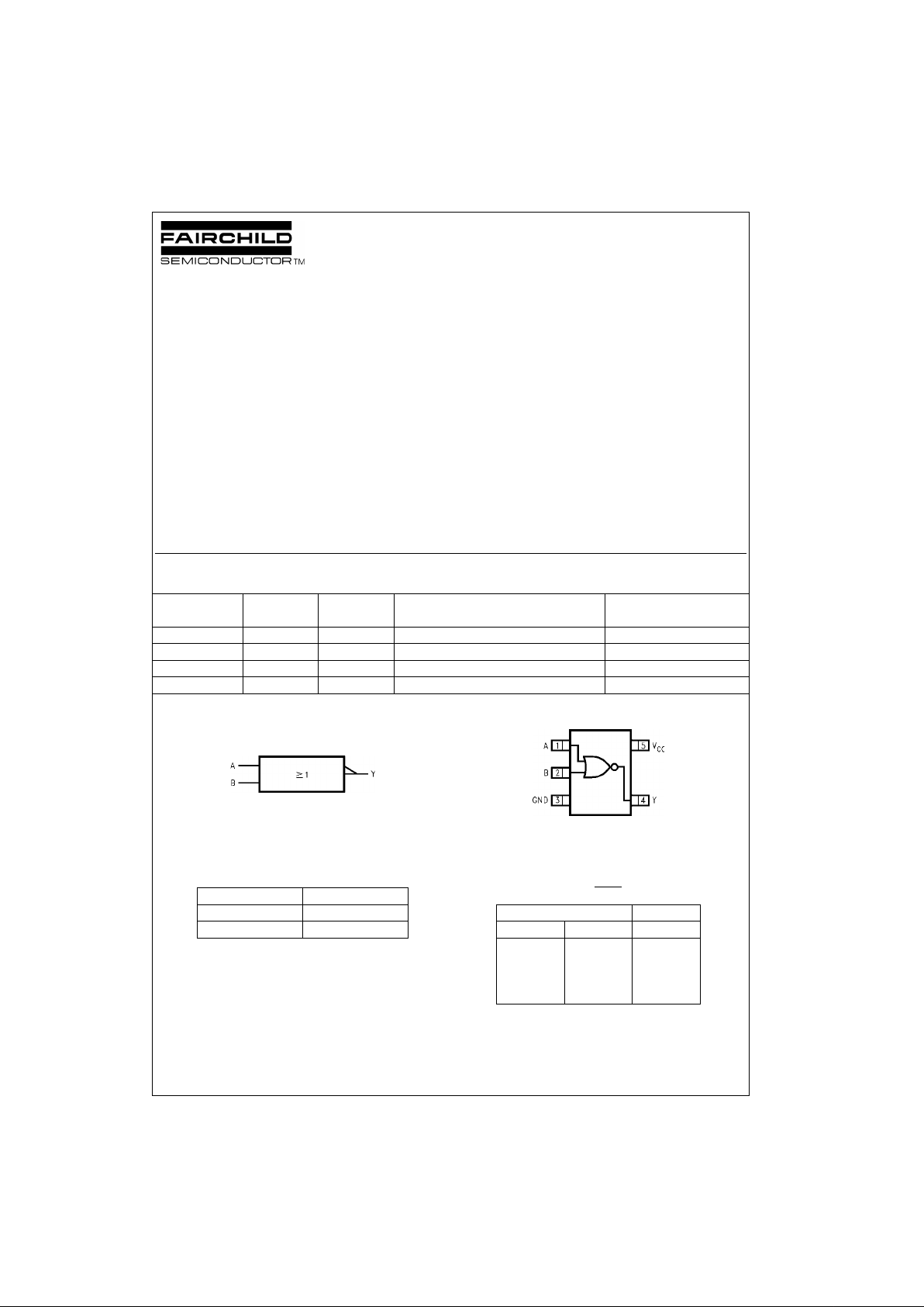
Logic Symbol
IEEE/IEC
Connection Diagram
(Top View)
Pin Descriptions Function Table
H = HIGH Logic Level
L = LOW Logic Level
TinyLogic is a trademark of Fairchild Semiconductor Co rporation.
Order Package Product Code
Package Descript ion Supplied As
Number Number Top Mark
NC7SZ02M5 MA05B 7Z02 5-Lead SOT23, JEDEC MO-178, 1.6mm 250 Units on Tape and Reel
NC7SZ02M5X MA05B 7Z02 5-Lead SOT23, JEDEC MO-178, 1.6mm 3k Units on Tape and Reel
NC7SZ02P5 MAA05A Z02 5-Lead SC70, EIAJ SC-88a, 1.25mm Wide 250 Units on Tape and Reel
NC7SZ02P5X MAA05A Z02 5-Lead SC70, EIAJ SC-88a, 1.25mm Wide 3k Units on Tape and Reel
Pin Names Description
A, B Inputs
Y Output
Y = A + B
Inputs Output
ABY
LLH
LHL
HLL
HHL
www.fairchildsemi.com 2
NC7SZ02
Absolute Maximum Ratings(Note 1) Recommended Operating
Conditions
(Note 2)
Note 1: Absolute maximum ratings are DC values beyond which the device
may be damage d or h ave its us eful life im paired . T he data shee t s pec ific ations should be met, without exception, to ensure that the system design is
reliable over its power supply, temperature, and output/input loading variables. Fairchild does no t recommend operation outsid e datasheet spec ifications.
Note 2: Unused inputs must be held HIGH or LOW. They ma y not float.
DC Electrical Characteristics
Supply Voltage (VCC) −0.5V to +6V
DC Input Voltage (V
IN
) −0.5V to +6V
DC Output Voltage (V
OUT
) −0.5V to +6V
DC Input Diode Current (I
IK
)
@ V
IN
< −0.5V −50 mA
@ V
IN
> 6V +20 mA
DC Output Diode Current (I
OK
)
@ V
OUT
< −0.5V −50 mA
@ V
OUT
> 6V, VCC = GND +20 mA
DC Output Current (I
OUT
) ± 50 mA
DC V
CC
/GND Current (ICC/I
GND
) ± 50 mA
Storage Temperature (T
STG
) −65°C to +150°C
Junction Temperature under Bias (T
J
) 150°C
Junction Lead Temperature (T
L
);
(Soldering, 10 seconds) 260
°C
Power Dissipation (P
D
) @ +85°C
SOT23-5 200 mW
SC70-5 150 mW
Supply Voltage Operating (V
CC
) 1.8V to 5.5V
Supply Voltage Data Retention (V
CC
) 1.5V to 5.5V
Input Voltage (V
IN
)0V to 5.5V
Output Voltage (V
OUT
) 0V to V
CC
Operating Temperature (TA) −40°C to +85°C
Input Rise and Fall Time (t
r
, tf)
V
CC
@ 1.8V, 2.5V ±0.2V 0 ns/V to 20 ns/V
V
CC
@ 3.3V ± 0.3V 0 ns/V to 10 ns/V
V
CC
@ 5.0V ± 0.5V 0 ns to 5 ns/V
Thermal Resistance (
θ
JA
)
SOT23-5 300
°C/W
SC70-5 425
°C/W
Symbol Parameter
V
CC
TA = +25°CT
A
= −40°C to +85°C
Units Conditions
(V) Min Typ Max Min Max
V
IH
HIGH Level Input Voltage 1.8 0.75V
CC
0.75V
CC
V
2.3–5.5 0.7 V
CC
0.7 V
CC
V
IL
LOW Level Input Voltage 1.8 0.25V
CC
0.25V
CC
V
2.3–5.5 0.3 V
CC
0.3 V
CC
V
OH
HIGH Level Output Voltage 1.8 1.7 1.8 1.7
VVIN = VILIOH=−100µA
2.3 2.2 2.3 2.2
3.0 2.9 3.0 2.9
4.5 4.4 4.5 4.4
2.3 1.9 2.15 1.9
V
IOH=−8mA
3.0 2.4 2.80 2.4 I
OH
=−16mA
3.0 2.3 2.68 2.3 I
OH
=−24mA
4.5 3.8 4.20 3.8 IOH=−32mA
V
OL
LOW Level Output Voltage 1.8 0.0 0.1 0.1
VVIN=VIHIOL=100µA
2.3 0.0 0.1 0.1
3.0 0.0 0.1 0.1
4.5 0.0 0.1 0.1
2.3 0.10 0.3 0.3
V
IOL= 8mA
3.0 0.15 0.4 0.4 IOL=16mA
3.0 0.22 0.55 0.55 IOL=24mA
4.5 0.22 0.55 0.55 IOL=32mA
I
IN
Input Leakage Current 0-5.5 ±1 ±10 µAVIN = 5.5V, GND
I
OFF
Power Off Leakage Current 0.0 1 10 µAVIN or V
OUT
= 5.5V
I
CC
Quiescent Supply Current 1.8-5.5 2.0 20 µAVIN = 5.5V, GND
3 www.fairchildsemi.com
NC7SZ02
AC Electrical Characteristics
Note 3: CPD is defined as the value of the internal equivalent capacitance which is derived from dynamic operating current consumption (I
CCD
) at no output
loading and operating at 50% duty cycle. (See Figure 2.) C
PD
is related to I
CCD
dynamic operating cu rrent by the expression:
I
CCD
= (CPD)(VCC)(fIN) + (ICCstatic).
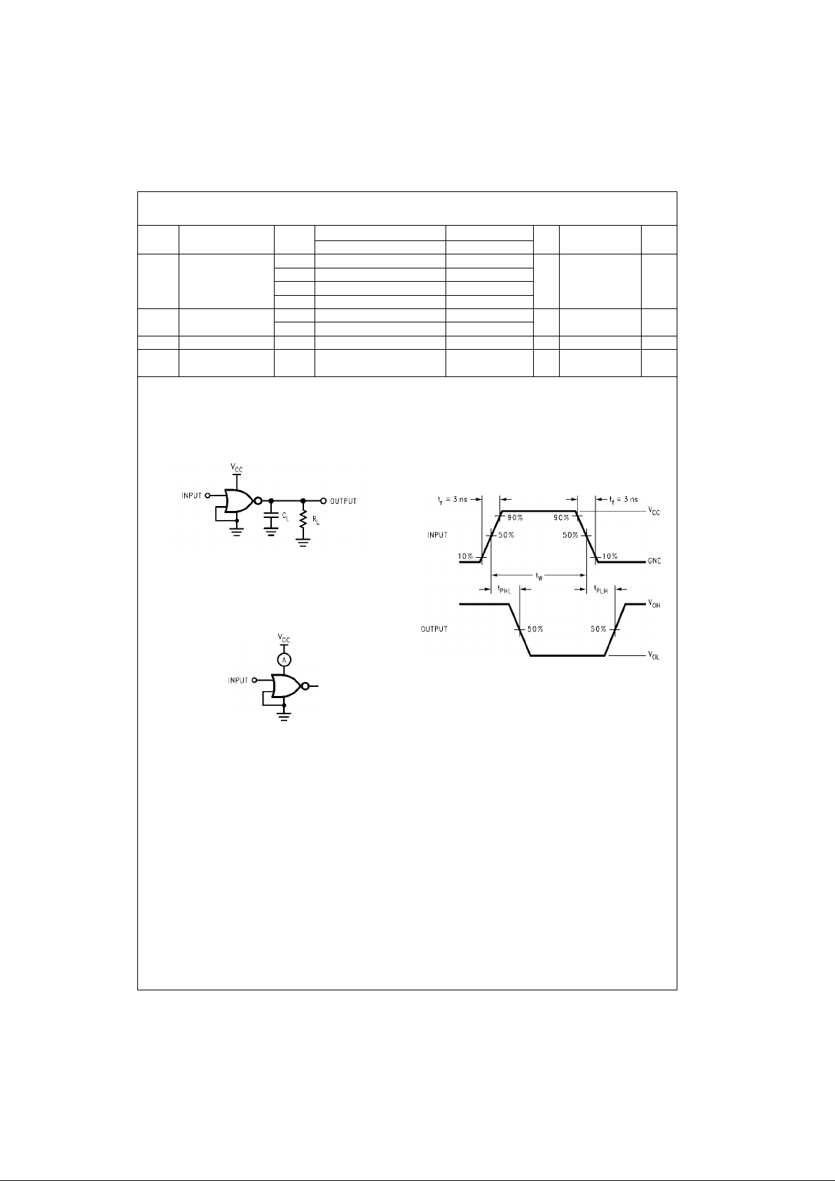
AC Loading and Waveforms
CL includes load and str ay capacitance
Input PR R = 1.0 MHz; t
w
= 500 ns
FIGURE 1. AC Test Circuit
Input = AC Waveform ; tr = tf = 1.8 ns;
PRR = 10 MHz; Duty Cycle = 50%
FIGURE 2. I
CCD
Test Circuit
FIGURE 3. AC Waveforms
Symbol Parameter
V
CC
TA = +25°CT
A
= −40°C to +85°C
Units Conditions Fig. No.
(V) Min Typ Max Min Max
t
PLH
, Propagation Delay 1.8 2.0 4.4 9.5 2.0 10
ns
Figures
1, 3
t
PHL
2.5 ± 0.2 0.8 2.9 6.5 0.8 7.0 CL = 15 pF,
3.3 ± 0.3 0.5 2.3 4.5 0.5 4.7 R
L
= 1 MΩ
5.0 ± 0.5 0.5 1.9 3.9 0.5 4.1
t
PLH,
Propagation Delay 3.3 ± 0.3 1.5 2.9 5.0 1.5 5.2
ns
CL = 50 pF,
Figures
1, 3
t
PHL
5.0 ± 0.5 0.8 2.4 4.3 0.8 4.5 RL = 500Ω
C
IN
Input Capacitance 0 4 pF
C
PD
Power Dissipation 3.3 23
pF (Note 3) Figure 2
Capacitance 5.0 30
 Loading...