


Service Manual
Service Manual
LCD Monitor 1907FPf
- 0 -
1
Service Manual Versions and Revision
No. |
Version |
Release Date |
Revision |
1 |
1.0 |
2006/6/03 |
Initial Release |
|
|
|
|
Copyright
Copyright 2006 InnoLux Display. Corp. Ltd
All Rights Reserved
This manual may not, in whole or in part, be copied, Photocopied, reproduced, translated, or converted to any electronic or machine readable form without prior written permission of Foxconn Tech. Corp. Ltd.
Dell 1907FFPf Service Manual

|
Service Manual |
|
|
|
Table of Contents |
|
|
CHAPTER 1- PRECAUTIONS & SAFETY NOTICES .................................................................................................................................... |
|
3 |
|
1. |
SAFETYPRECAUTIONS....................................................................................................................................................................... |
|
3 |
2. |
PRODUCT SAFETY NOTICE ............................................................................................................................................................... |
|
3 |
3. |
SERVICE NOTES ..................................................................................................................................................................................... |
|
3 |
CHAPTER 2- SERVICE TOOLS & EQUIPMENT REQUIRED .................................................................................................................. |
|
4 |
|
CHAPTER 3- CIRCUIT THEORY......................................................................................................................................................................... |
|
5 |
|
1. |
BLOCK DIAGRAM ....................................................................................................................................................................................... |
|
5 |
2. |
ELECTRONIC CIRCUIT THEORY................................................................................................................................................................. |
|
6 |
3. |
FACTORY PRESET TIMING TABLE .................................................................................................................................................. |
|
8 |
4. |
POWER ON/OFF SEQUENCY...................................................................................................................................................................... |
|
9 |
5. |
D-SUB CONNECTOR PIN ASSIGNMENT................................................................................................................................................... |
|
7 |
6. |
AC OUTLET PIN ASSIGNMENT................................................................................................................................................................ |
|
10 |
7. |
INNER CONNECTOR PIN ASSIGNMENT ................................................................................................................................................... |
|
11 |
8. |
KEY PARTS PIN ASSIGNMENTS................................................................................................................................................................ |
|
13 |
CHAPTER 4- DISASSEMBLY & ASSEMBLY ................................................................................................................................................. |
|
19 |
|
1. |
EXPLODED DIAGRAM............................................................................................................................................................................... |
|
19 |
2. |
1707FPF DISASSEMBLY BLOCK.............................................................................................................................................................. |
|
20 |
3. |
ASSEMBLY BLOCK.................................................................................................................................................................................... |
|
21 |
CHAPTER 5- TEST AND ADJUSTMENT ......................................................................................................................................................... |
|
21 |
|
1. |
FUNCTION KEY DEFINITIONS.................................................................................................................................................................. |
|
22 |
2. |
OSD CONTROL .................................................................................................................................................. |
! |
|
3. |
FACTORY MODE INTRODUCTION............................................................................................................................................................ |
|
22 |
4. |
BURN-IN PATTERN..................................................................................................................................................................................... |
|
23 |
5. |
AUTO COLOR BALANCE (AUTOMATICALLY CALIBRATE CHIPADC PARAMETER BY USING CHIP INTERNAL DAC.) .................. |
23 |
|
6. |
EDID (REWRITE EDID DATA TO EEPROM)........................................................................................................................................ |
|
23 |
7. |
UPLOAD FIRMWARE VIA VGA CABLE.................................................................................................................................................... |
|
30 |
8. |
AFTER REPAIR, TO ENSURE THE QUALITY YOU SHOULD DO THE FOLLOWING TEST AND ADJUSTMENT......................................... |
|
32 |
CHAPTER 6- TROUBLE SHOOTING ............................................................................................................................................................... |
|
35 |
|
1. |
COMMON ACKNOWLEDGE................................................................................................................................ |
! |
|
2. |
NO POWER & POWER LED OFF ............................................................................................................................................................. |
|
35 |
3. |
POWER LED AMBER................................................................................................................................................................................ |
|
38 |
4. |
BACKLIGHT CAN’T BE TURNED ON......................................................................................................................................................... |
|
39 |
5. |
NO PICTURE & BACKLIGHT ON............................................................................................................................................................... |
|
40 |
6. |
AT 32-GRAY SCALE PATTERN, COLOR LOST IN SOME SCALE................................................................................................................ |
|
41 |
ATTACHMENT 1- BILL OF MATERIAL................................................................................................................... |
! |
||
ATTACHMENT 2- SCHEMATIC ......................................................................................................................................................................... |
|
55 |
|
ATTACHMENT 3- PCB LAYOUT ........................................................................................................................................................................ |
|
70 |
|
2

Service Manual
Chapter 1- PRECAUTIONS & SAFETY NOTICES
SAFETY PRECAUTIONS
This monitor is manufactured and tested on a ground principle that a user’s safety comes first. However, improper used or installation may cause damage to the monitor as well as to the user.
WARNINGS:
•This monitor should be operated only at the correct power sources indicated on the rating label on the rear cover of the monitor. If yo u’re unsure the power supply in your residence, consult your local dealer or Power Company.
•Use only the specified power cord that comes with this monitor.
•Do not try to repair the monitor by yourself, as it contains no user-serviceable parts. This monitor should only be repaired by a qualified technician.
•Do not remove the monitor cabinet. There is highvoltage parts inside that may cause electric shock to human bodies.
•Stop using the monitor if the cabinet is damaged. Have it checked by a service technician.
•Put your monitor only in a lean, cool, dry environment. If it gets wet, unplug the power cable immediately and consult your closed dealer.
•Always unplug the monitor before cleaning it. Clean the cabinet with a clean, dry cloth. Apply non-ammonia based cleaner onto the cloth, not directly onto the class screen.
•Do not place heavy objects on the monitor or power cord.
PRODUCT SAFETY NOTICE
Many electrical and mechanical parts in this chassis have special safety visual inspections and the protection afforded by them cannot necessarily be obtained by using replacement components rated for higher voltage, wattage, etc. Before replacing any of these components read the parts list in this manual carefully. The use of substitute replacement parts, which do not have the same safety characteristics as specified in the parts list, may create shock, fire, or other hazards.
SERVICE NOTES
•When replacing parts on circuit boards, clamp the solder wires around terminals before soldering.
•Keep wires away from high voltage, high temperature components and sharp edges.
•Keep wires in their original position so as to reduce interference.
•Adjustment of this product please refers to the user’manual.
•Use Pb free solder wire for circuit board preparation.
3

Service Manual
Chapter 2- SERVICE TOOLS & EQUIPMENT REQUIRED
1.SIGNAL GENERATOR
2.MULTIMETER
3.SCREW DRIVER
4.OSCILLOSCOPE
5.Soldering IRON
6.SOLDER (Lead free, RoHS compliance)
7.Color Analyzer
8.Fox_VISP_Programmer
9.Fox_VEDID_Programmer
4

Service Manual
Chapter 3- CIRCUIT THEORY
1. Block Diagram
There are 4 pieces PCBA in monitor, one is power/inverter board which is single layer board, one is Interface board with USB HUB (1up/2down) which is two layers board, one is keypad board, one is USB transfer board located on side of monitor.
TFT LCD Panel 17
M170EG01 (AUO)
|
|
|
|
|
|
|
|
LM170E01-TLB3/B4 (LPL) |
|
|
|
|
|
|
|
|
|
|||
|
|
|
|
Backlight ON-OFF/Brightness CTRL |
|
|
|
CN501 |
|
|
|
|
||||||||
CN3 |
|
|
|
+5V |
|
|
|
|
|
|
|
|
|
|
|
|
|
|||
|
|
|
|
|
|
|
|
|
|
|
|
|
|
|
|
|
|
|||
|
|
|
+16V |
|
|
|
|
|
|
|
|
|
|
|
|
|
|
|
||
|
|
|
|
|
|
|
|
|
|
|
|
|
|
|
|
|
|
|
||
CN4 |
|
|
|
|
|
|
|
|
|
|
|
|
DC-DC |
|
|
Power 5V |
|
|
|
|
|
T2 |
|
|
SNUBBER |
|
|
|
D854 |
|
5V |
|
|
for Panel |
|
|
|
|
|||
|
|
|
|
|
|
|
|
|
5V-3.3V |
|
|
|
|
|
|
|||||
|
|
|
|
|
|
|
|
|
|
|
|
|
|
|
|
|
||||
|
|
|
|
Charge |
4 . |
|
|
|
|
3.3V-1.8V |
|
|
|
U403 |
|
|
|
|||
|
|
|
|
Q850 |
pump |
|
|
|
|
|
|
|
|
|
|
|||||
AP9971G AP9971G |
|
|
|
|
|
|
|
|
|
|
|
|
|
|
|
|
||||
|
|
|
|
|
|
|
|
|
|
|
|
24C16 |
|
|
|
|||||
|
|
|
AP2761 |
6 |
|
8 |
|
DC-DC |
|
|
|
|
|
|
|
|||||
|
|
|
|
|
+16V |
|
|
|
|
|
|
|
||||||||
Q6 Q7 |
|
|
|
|
|
9 |
16V-5 V |
|
|
|
|
|
|
|
318MHz.14 |
|
||||
|
|
|
|
|
|
|
|
|
|
|
|
|
|
|
|
|
||||
OZ9936G |
|
|
|
Current |
|
. |
11 |
|
|
|
|
|
U401 |
|
|
|
XTAL |
|||
|
|
sense |
1 |
12 |
|
|
|
|
|
|
|
|
||||||||
|
|
|
|
|
|
|
|
|
|
|
|
|||||||||
|
|
|
|
|
|
|
|
|
|
|
|
|
||||||||
U1 |
U850 |
2 |
. |
|
1 |
|
|
|
|
Gm5621-LF |
|
|
||||||||
|
2 |
|
|
|
|
|
|
|||||||||||||
|
|
|
|
|
|
|
|
|||||||||||||
SG6841 |
|
|
3 |
|
|
|
|
|
|
|
|
|||||||||
|
|
T850 |
|
|
|
|
U402 |
|
R. G. B. H. V |
|
||||||||||
|
|
|
|
|
|
|
Serial flash |
|
|
|||||||||||
|
|
|
|
|
OVP |
|
|
|
|
|
|
|
24MHz |
XTAL |
|
|||||
|
|
|
|
|
|
|
|
|
|
|
|
|
|
|
|
|
||||
|
|
|
|
|
|
|
|
I850 |
|
|
|
|
|
|
|
|
|
|||
|
|
|
|
4 |
1 |
|
|
817B |
|
|
|
|
U301 |
|
|
|
|
|||
|
|
|
|
- |
+ |
|
|
|
|
|
|
|
|
|
|
|||||
|
|
T1 |
|
3 2 |
|
|
|
|
CN401 |
|
|
ESD |
|
|
|
|||||
|
|
|
|
|
|
|
|
|
|
|
24C02 |
|
|
P001, |
||||||
CN2 |
|
|
|
D850 |
|
|
|
|
|
|
|
Protection |
U901 |
|||||||
|
|
|
|
|
|
|
|
U302 |
|
|
|
|||||||||
|
|
|
|
|
|
AC Line-in |
DC-DC |
|
|
DDC_CLK |
|
SMSC |
|
|
P002 |
|||||
|
|
|
|
|
|
16V-12V |
|
|
24C02 |
|
|
|
||||||||
CN1 |
|
|
|
|
|
|
filter |
|
|
|
DDC_DATA |
|
|
|
|
|||||
|
|
|
|
|
|
|
|
|
|
|
|
|
|
|
||||||
|
|
|
|
|
|
|
|
|
|
|
|
|
|
|
|
|
|
|
||
|
|
|
|
|
CN850 |
|
|
|
|
|
|
CN302 |
|
CN301 |
USB Hub |
|
|
|
|
|
|
|
|
|
|
AC Socket |
|
|
|
|
|
|
|
P902 |
|
|
|||||
|
|
|
|
|
|
|
|
|
|
CN853 |
|
|
DVI |
|
D-SUB |
P901 |
|
|
||
|
|
|
|
|
|
|
|
|
|
|
|
|
|
|
|
|||||
|
|
|
|
|
AC 90V-240V |
|
Audio |
|
|
Digital |
Analog |
PC Hub |
|
|
|
|
||||
|
|
|
|
|
Input |
|
|
|
Function Key |
|
Device |
|
||||||||
|
|
|
|
|
|
|
|
|
|
|
||||||||||
|
|
|
|
|
|
|
|
|
|
|
Board |
|
Video Input |
Video Input |
Input |
|
|
|
|
|
5

Service Manual
2. Electronic Circuit Theory
2.1Switching Mode Power Supply
2.1.1 AC Current Input Circuit
CN850 is a connector for connecting Ac Power. F850 is a fuse to protect all the circuit Ac. Input voltage is from 90v to 264V. R850 and R851 in serial to prevent man from shock. L851 is used to clear up low frequency wave. C850 and C851 are used to discharge the waves that L851 produced. High frequency waves are damped by C852 and C853. D850 is a rectifier in which there are 4 buildin diodes, inverting AC to DC.
2.1.2 High Voltage to Low Voltage Control Circuit
C854 is used to smooth the wave from rectifier. R852 is a fuse to protect the following circuit when current flow is too large. U850 is a highly integrated PWM controller. Typical start-up current for U850 is only 30 uA, R853 and R854 are serial circuit to limit current flow. When current flow through R853 and R854 gets to Pin 3 of U850, with VDD hold-up capacitor C857, U850 is enough for starting up.
When U850 begins to work Pin8 of U850 will output about 18v to drive Q850,and then the main current flow get to GND bypassing through T850, Q850. Because of the change of current flow, wires in the other side of T850 will induct current.At the same time, the current inducted by wires which connected T850 Pin 1 and Pin 2, with components of D852, R855, C857 and C856, will be supplied to U850 for normal operating.
When the sense voltage across the sense resistor R859, reaches the threshold voltage around 0.85v, the output GATE drive will be turned off. Every time when the output of power supply is shorted or over loaded, the FB voltage will increase, the buildin PWM output will then be turned off. Both will prevent the power supply from being overheated under over loading condition. The PWM duty cycle is determined by this current sense signal and VFB, the feedback voltage. When the voltage on sense pin reaches Vcomp =(VFB-1.0)/3, A switch cycle will be terminated immediately. Vcomp is internally clamped to a variable voltage around 0. 85 V for output power limit
When Q850 are turned off, the main current flow will be consumed through D851, C880 and R880. This will prevent Q850 from being damaged under large current impulse and voltage spike.
2.1.3 DC_12V Output Circuit
D854 is used to rectify the inducted current. R860 and C861 are used to store energy when current is reversed. The parts including C862, C864, C863 and L853 are used to smooth the current waves that are from D854, and then 12- v voltage is supplied
12-v supply voltage feed back to PWM controller U850 via R863, R868, and I850,I851.
2.1.4 Protect Circuit of U850
When Vdd or 12V output come out of SPEC , the voltage on D856 will be rised over 22 volts, the current via D856 is large enough to star up protect circuit internal U850, U850 will be in Auto Restart mode until the matter is got rid of .
2.2 Inverter Circuit
2.2.1 Low voltage to High voltage circuit
DC_5V through R2 will provide power for U1 on the pin6. EN-ON/OFF voltage signal coming from gm2621LF which is on IF BD will enable Q1 and Q2 to work. R5 and R30 are used to limit current. C5 is used to dump noise, C6 is used to soft start, and then the voltage on pin 1 will enable U1. The operating frequency is determined by the external resistor (R4) connected to Pin 2.
During start up, VSEN-DIM (pin7) senses the voltage on the transformer secondary. When VSEN reaches 3V, the output voltage is regulated. If no current is sensed approximately 2 seconds, U1 shuts off. DIM-ADJ duty cycle signal through R3 and C5 is on Pin 7(ISEN), which adjusted will can change the brightness of Panel.
DRV1 and DRV2 of U1 are used to drive Q6 and Q7 . DRV1 and DRV2 are controlled by buildin PWM IC. Q6 and Q7 are switches which has two build-in IGBTs. The working principle of circuit of T1 and T2, Q6 AND Q7 are the same to circuit of T850 and Q850 described ahead.
6

Service Manual
The voltage signal on Pin2 of ZD4 sensed through R14 comes to Pin8 of U1, ISEN (Lamp Current Detection & Control). C12 is used to dump noise. Once the CCFLs are ignited and current is sensed through resistor R14 ,capacitor C12 performs the loop compensation function. The voltage at pin 1 controls the drive duty cycle of the power MOSFETs to regulate the CCFL current.
2.2.2 Protection Circuit of U1
If a CCFL is removed, fails or damaged during normal operation, CCFL current is no longer sensed and the voltage on ISEN pin drops. Once the voltage at the ISEN pin is less than the lamp” on” threshold, the shutdown timer is activated. The IC maintains the output voltage for approximately 2-3seconds and once the timer expires, the IC will shutdown. To restart the IC, either toggle the ENA_SST_CMP pin or recycle the power on the VDDA pin.
The control logic protects the transformer from an abnormally high voltage at the secondary output.T1and T2 output voltage are sensed through Rectifier Diodes Q3.When the voltage at the emitter of Q3 is less than –Vbe DROP,Q3 will conduct and regulate the output voltage to T1and T2 secondary.
2.3 I/F Board Circuit
2.3.1 RGB CAPTURE
-Signal RED,GREEN,BLUE input through CN301 #1,#2,#3, Stop DC via C303, C302 and C301, and then enter into U401 (gm5621-LF) analog input terminal #99,#96,#93, and then gm5621-LF deals with signal internally. D315, D316, D317 are ESD protector to prevent U401 from ESD.
-Signal DDC_SCL (series clock) inputs via CN301#15, and then passes through ZD304 for ESD protection, goes into EDID EEPROM IC U301 #6.
-Signal DDC_SDA (series data) inputs via CN301#12, and then passes through ZD306 for ESD protection, goes into EDID EEPROM IC U301 #5.
-Signal TTL vertical sync. (Vsync) inputs via CN301 #14, and then clamped by ZD302 Zener, passes
through R311, and then goes into IC U401 (gm5621-LF) #90.
-Signal TTL horizontal sync. (Hsync) inputs via CN301 #13, and then clamped by ZD301 Zener, passes through R310, and then goes into IC U401 (gm5621-LF) #89.
-CN301#5 is defined as cable detect pin, this detector realize via R337 and U401#114, and ZD306 is ESD protector.
-U301 +5V is supplied by PC via CN301#9 with D328 and ZD303 for ESD protection, or supplied by Monitor self via D304.
-U301 is an EEPROM IC which is memory and VGA input EDID data saved in it.
2.3.2 DVI CAPTURE
- Differential Signal input RX0+,RX0-,RX1+,RX1-,RX2+,RX2-,RXC+,RXC- through CN302 #18,#17,#10,#9,#2,#1,#23,#24 via R330,R327,R318,R321,R317,R303,R331,R335 enter into U401 (gm5621) Digital input terminal #80,#81,#75,#76,#72,#73,#83,#84, and then gm5621 deals with signal internally.
-Signal DDC_SCL (series clock) inputs via CN302#6, and then passes through ZD307 Zener for ESD protection, via R328, goes into EDID EEPROM IC U302 #6.
-Signal DDC_SDA (series data) inputs via CN302#7, and then passes through ZD308 Zener for ESD protection, via R329, goes into EDID EEPROM IC U301 #5.
-CN302#15 is defined as cable detect pin, this detector realize passes through R339 ,go into U401#114, and ZD309 is ESD protector.
-U302 +5V is supplied by PC via CN302#15 through D330, or supplied by Monitor self via D329.
-U302 is an EEPROM IC which is memory and DVI input EDID data saved in it.
2.3.3 Buttons Control
-Button “Power” on front bezel connects to U401 (gm5621-LF) #125 through CN401 #1, U401 #125 is defined as power on/off.
-Button “+” on front bezel connects to U401 (gm5621-LF) #115 through CN401 #4 via R431
U401 #115 (LBADC control Pin ) is defined as “UP”.
- Button “-” on front bezel connects to U401 (gm5621-LF) #115 through CN401 #5 via R429
7

Service Manual
U401 #115 (LBADC control Pin ) is defined as “DOWN ”.
-Button “Menu” on front bezel connects to U401 (gm5621-LF) #113 through CN401 #6 via R427, U401 #113 ((LBADC control Pin ) is defined as “Menu”.
Button “Select” on front bezel connects to U401 (gm5621-LF) #113 through CN401 #7 via R428, U401 #113 (LBADC control Pin ) is defined as “S elect”.
-LED Indicator on Front Bezel
a.When press button “power”, U401(Scalar) #125 be send in low potential, make U401#51 sends out high potential through CN401 #3 via R406 to J1#3 on keypad, LED Green on.
b.When in “Suspend ” mode, U401 (Scalar) #57 sends out a high potential through CN401 #2 via R404 to J1#2 on keypad .LED Amber ON.
2.3.4 GENESIS CHIP U401 (gm2621-LF)
-U401 (gm5621-LF) #7~#16. #31~#40 output 8 bit even LVDS digital data to panel control circuit through CN501.
-U401 (gm5621-LF) #127 output PPWR ”H” potential to make Q502 conducted, and then make Q501 conducted, +5V flow to CN501#1~#3 as Panel Vdd .
-U401 (gm5621-LF) #49 output CCFL_ON/OFF ”H” potential to control Inverter on/off.
-U401 (gm5621-LF) #50 outputs Brightness “PWM” signals to control CCFL brightness.
-TCLK by Crystal 14.318MHz input to U401 (gm5621-LF) #109.
-U401 (gm5621-LF) #111 Bidirectional RESET signals
Please refer to gm5621-LF Pin Assignments table in page
2.3.5 Regulator Circuit
-- +5V is from power supply for U301, U302, U601,U902, U904, U905 and Panel used.
-+3.3V is from switching mode power supply for U401,U402, U404,U901,U903
-+1.8V generates from +3.3V through C603 filtering and U602 which is output +1.8V LDO, for U401 used.
2.3.6 USB circuit
-USB Signal input D+,D- through P901,#3,#2, then enter into U901 (SMSC2504) Signal input terminal #2,#3, and then SMSC2504 deals with signal internally.
-U901 (SMSC2504) #5,#6, #8,#9 output DD+[1],DD-[1], DD+[2],DD-[2] USB data through P902 #6,#7,#3,#2 . EP901, EP902,EP905,EP906 are ESD protector
-U901 (SMSC2504) #11,#12, #15,#14 output DD+[3],DD-[3], DD+[4],DD-[4] USB data through CN901 #3,#4, #8,#7 .
-In normal condition,U901(SMSC2504) #45,#43,#39,#37 output low signal to U904 (G556) #1,#4,
U905 (G556) #1,#4, then U904 and U905 #8,#5 output 5v to provide downstream power. When the loading is over current, U904 (G556) #2,#3, U905 (G556) #2,#3 output Activelow signal to U901 #46,#44, #40,#38,then U904,U905 output power will be cut off.
-Xin by Crystal 24MHz input to U901 (SMSC2504) #58.
3.FACTORY PRESET TIMING TABLE
3.1Analog
|
Standard |
|
Resolution |
Horizontal Frequency |
Vertical Frequency |
|
|
|
|
(KHz) |
(Hz) |
|
|
|
640 x 480 |
31.469 |
59.940 |
|
|
|
640 x 480 |
37.500 |
75.000 |
|
|
|
|
|
|
|
|
|
800 x 600 |
37.879 |
60.317 |
|
|
|
|
|
|
|
VESA |
|
800 x 600 |
46.875 |
75.000 |
|
|
1024 x 768 |
48.363 |
60.004 |
|
|
|
|
|||
|
|
|
|
|
|
|
|
|
1024 x 768 |
60.023 |
75.029 |
|
|
|
|
|
|
|
|
|
1280x1024 |
48.483 |
60.042 |
|
|
|
1280x1024 |
60.087 |
75.034 |
|
|
|
|
|
|
|
IBM DOS |
|
720 x 400 |
31.469 |
70.087 |
|
|
|
|
8 |
|

|
|
|
|
|
|
Service Manual |
|
|
3.2 Digital |
|
|
|
|
|
|
|
|
|
|
|
|
|
|
|
|
Standard |
|
Resolution |
Horizontal Frequency |
Vertical Frequency |
|
|
|
|
|
|
(KHz) |
(Hz) |
|
|
|
|
|
640 x 480 |
31.469 |
59.940 |
|
|
|
|
|
|
|
|
|
|
|
VESA |
|
800 x 600 |
37.879 |
60.317 |
|
|
|
|
1024 x 768 |
48.363 |
60.004 |
|
|
|
|
|
|
|
|||
|
|
|
|
|
|
|
|
|
|
|
|
1280x1024 |
48.483 |
60.042 |
|
4. Power On/Off Sequency
Hardware Power ON
When power cord plug into AC socket, Power provides 12V. DC_5V, DC_3.3V generate from DC_12V through LDO U851.DC_5V is voltage for panel and USB IC U901, DC_3.3v is main voltage for U401. When DC_3.3V input to U401, U401 reset circuit active, set U401 all registers to default,. That means finish hardware power on.
Software Power ON/OFF
When press power key, U401 #125 recieves low pulse, and then (gm5621-LF) U401 will be wake up and send high puls(at 127,49pin) to on CCFL and switch 5.0v to panel module. And make the VGA cable input signal source display normal on panel.
-If Power ON, U402 #51 (LED_Green) will send out High potential, and then LED green on.
-If Power OFF, U402 #57 (LED_Amber) will send out High potential, and then LED Amber on. The Panel_Vcc, Backlight_En, CLK/DATA output to panel will follow the following sequency.
Power supply for VDD |
|
|
|
|
|
|
|
|
|
|
|
|
|
|
|
|
|
|
|
|
|
|
|
|
|
|
0V |
10% |
|
|
|
|
|
|
90% |
90% |
|
|
|
|
|
|
10% |
|
|
|
|
|
|||||
|
|
|
|
|
|
|
|
|
|
|
|
|
|
|
|
|
||||||||||
|
|
|
|
|
|
|
|
|
|
|
|
|
|
|
|
|
|
|
|
|
|
|
||||
|
|
|
|
|
|
|
|
|
|
|
|
|
|
|
|
|
|
|
|
|
|
|
|
|||
|
|
|
|
|
|
|
|
|
|
|
|
|
|
|
|
|
|
|
|
|
|
|
|
|||
|
|
|
|
T1 |
|
|
T2 |
|
|
|
|
|
|
|
|
|
|
|
|
|
|
|
|
|
||
|
|
|
|
|
|
|
|
|
T5 |
|
T6 |
|
|
|
|
|
|
|
||||||||
Signals |
|
|
|
|
|
|
|
|
|
|
|
|
|
|
T7 |
|
|
|
|
|
||||||
|
|
|
|
|
|
|
|
|
|
|
|
|
|
|
|
|
|
|
|
|
|
|
|
|
||
|
|
|
|
|
|
|
|
|
|
|
|
|
|
|
|
|
|
|
|
|
|
|
|
|
||
|
|
|
|
|
|
|
|
|
|
|
|
|
|
|
|
|
|
|
|
|
|
|
|
|
||
|
|
|
|
|
|
|
|
|
Valid data |
|
|
|
|
|
|
|
|
|
|
|
|
|
||||
(Digital RGB, HS, VS, DE, CLOCK) |
|
|
|
|
|
|
|
|
|
|
|
|
|
|
|
|
|
|
|
|||||||
|
|
0V |
|
|
|
|
|
|
|
|
|
|
|
|
|
|
|
|
|
|
|
|||||
|
|
|
|
|
|
|
|
|
|
|
|
|
|
|
|
|
|
|
|
|
|
|
|
|
|
|
|
|
|
|
|
|
|
|
|
|
|
|
|
|
|
|
|
|
|
|
|
|
|
|
|
|
|
|
|
|
|
|
|
|
|
|
|
|
|
|
|
|
|
|
|
|
|
|
|
|
|
|
|
|
|
|
|
|
|
|
|
|
|
|
|
|
|
|
|
|
|
|
|
|
|
|
|
|
|
|
|
|
|
|
|
|
|
|
|
|
|
|
|
|
|
|
|
|
|
|
|
|
|
|
|
|
|
|
T3 T4
Power supply for back light
|
T1(ms) |
T2 (ms) |
T3 (ms) |
T4 (ms) |
T5 (ms) |
T6 (ms) |
T7(ms) |
SPEC(AU) |
0.0~10 |
0.5~50 |
>200 |
>200 |
0.5~50 |
0.5~10 |
>1000 |
SPEC(LPL) |
0.5~10 |
0~50 |
>200 |
>200 |
0.0~50 |
0.5~10 |
>1000 |
9
Service Manual
5. D-SUB Connector Pin Assignment
Pin |
Symbol |
Pin |
Symbol |
Pin |
Symbol |
1 |
Red |
6 |
Red_GND |
11 |
GND |
2 |
Green |
7 |
Green_GND |
12 |
DDC_SDA |
3 |
Blue |
8 |
Blue_GND |
13 |
Hsync |
4 |
GND |
9 |
PC+5V |
14 |
Vsync |
5 |
Cable Detect |
10 |
GND |
15 |
DDC_SCL |
6. AC Outlet Pin Assignment
|
2 |
|
|
|
|
|
|
|
|
|
|
|||||
|
|
|
|
|
|
|
|
|
|
|
|
|
|
|
Pin |
Symbol |
|
|
|
|
|
|
|
|
|
|
|
|
|
|
|
||
1 |
|
|
|
|
|
|
|
|
|
|
|
|
3 |
|
1 |
Line |
|
|
|
|
|
|
|
|
|
|
|
|
|
|
|
2 |
GND |
|
CN850 |
3 |
Neutral |
|||||||||||||
7. DVI Connector Pin Assignment
Pin# |
Symbol |
Description |
1 |
TX 2 - |
TMDS Negative differential input, channel 2 |
2 |
TX 2 + |
TMDS Positive differential input, channel 2 |
3 |
SHLD 2 / 4 |
Shield for TMDS channels 2 / 4 |
4 |
TX 4 - |
TMDS Data 4 - |
5 |
TX 4 + |
TMDS Data 4 + |
6 |
DDC Clk |
DDC Clock |
7 |
DDC Data |
DDC Data |
8 |
AVS |
Analog Vertical Sync |
9 |
TX 1 - |
TMDS Data 1 - |
10 |
TX 1 + |
TMDS Data 1 + |
11 |
SHLD 1 / 3 |
TMDS Data 1 / 3 Shield |
12 |
TX 3 - |
TMDS Data 3 - |
13 |
TX 3 + |
TMDS Data 3 + |
14 |
+5V |
+5V Power |
15 |
GND |
Ground (Return for +5V, Hsync, and V Sync) |
16 |
HPD |
Hot Plug Detect |
17 |
TX 0 - |
TMDS Data 0 - |
18 |
TX 0 + |
TMDS Data 0 + |
19 |
SHLD 0 / 5 |
TMDS Data 0 / 5 Shield |
20 |
TX 5 - |
TMDS Data 5 - |
21 |
TX 5 + |
TMDS Data 5 + |
22 |
TX CLK SHLD |
TMDS Clock Shield |
23 |
TX CLK + |
TMDS Clock + |
24 |
TX CLK - |
TMDS Clock - |
10

Service Manual
8. USB Up stream Connector pin assignment (B type)
Pin# |
Symbol |
Description |
1 |
VBUSPWR |
USB Cable detect, PC_+5V |
2 |
DM |
|
3 |
DP |
|
4 |
GN |
Ground |
5 |
SHELL |
Ground |
9. USB Down stream connector pin assignment (A type) P902
Pin# |
Symbol |
Description |
1 |
PWR2 |
|
2 |
DD2M |
|
3 |
DD2P |
|
4 |
GND |
|
5 |
PWR1 |
|
6 |
DD1M |
|
7 |
DD1P |
|
8 |
GND |
Ground |
9 |
SHELL |
Ground |
10. USB Down stream connector pin assignment (A type) P001, P002
Pin# |
Symbol |
Description |
1 |
GND |
|
2 |
DD4P/DD3P |
|
3 |
DD4M/DD3M |
|
4 |
PWR4/PWR3 |
|
11.Inner Connector Pin Assignment
11.1CN501 (Connect M/B to Panel, AL2309-A0K0D-P or compatible connector)
Pin |
Symbol |
Description |
1 |
Panel_Vcc |
Panel power supply (typ.5.0V) |
2 |
Panel_Vcc |
Panel power supply (typ. 5.0V) |
3 |
Panel_Vcc |
Panel power supply (typ. 5.0V) |
4 |
NC |
|
5 |
NC |
|
6 |
NC |
|
7 |
GND_LVDS |
LVDS Ground |
8 |
RXE3+ |
LVDS signal of even channel 3(-) |
9 |
RXE3- |
LVDS signal of even channel 3(+) |
10 |
RXEC+ |
LVDS signal of even channel clock (+) |
11 |
RXEC- |
LVDS signal of even channel clock (-) |
12 |
RXE2+ |
LVDS signal of even channel 2(+) |
13 |
RXE2- |
LVDS signal of even channel 2(-) |
14 |
GND_LVDS |
LVDS Ground |
15 |
RXE1+ |
LVDS signal of even channel 1(+) |
16 |
RXE1- |
LVDS signal of even channel 1(-) |
17 |
GND_LVDS |
LVDS Ground |
18 |
RXE0+ |
LVDS signal of odd channel 0(+) |
19 |
RXE0- |
LVDS signal of odd channel 0(-) |
20 |
RXO3+ |
LVDS signal of odd channel 3(+) |
21 |
RXO3- |
LVDS signal of odd channel 3(-) |
22 |
RXOC+ |
LVDS signal of even channel clock (+) |
23 |
RXOC- |
LVDS signal of even channel clock (-) |
|
|
11 |

Service Manual
24 |
GND_LVDS |
LVDS Ground |
25 |
RXO2+ |
LVDS signal of even channel 2(+) |
26 |
RXO2- |
LVDS signal of even channel 2(-) |
27 |
RXO1+ |
LVDS signal of even channel 1(+) |
28 |
RXO1- |
LVDS signal of even channel 1(-) |
29 |
RXO0+ |
LVDS signal of odd channel 0(+) |
30 |
RXO0- |
LVDS signal of odd channel 0(-) |
11.2 CN1, CN2, CN3, CN4 (Connect to Panel Backlight, SM02B-BHSS-1-TB or compatible connector)
Pin |
Symbol |
Description |
1 |
HV |
High voltage for lamp |
2 |
LV |
Low voltage for lamp |
11.3 CN401 (Connect IF to keypad S8B-PH-K or compatible connector)
Pin |
Symbol |
Description |
1 |
Audio Detect |
Sound bar detect pin |
2 |
LED Amber |
LED Green on/off control |
3 |
LED Green |
LED amber on/off control |
4 |
UP |
keypad “+” control |
5 |
DOWN |
Keypad “-” control |
6 |
MENU |
Keypad “MENU” control |
7 |
Select |
Input signal Select |
8 |
GND |
GND |
11.4 CN601 (Connect Power/Inverter with IF board)
|
Pin |
Symbol |
|
|
Description |
|
|
1 |
GND |
GND |
|
|
|
|
2 |
GND |
GND |
|
|
|
|
3 |
GND |
GND |
|
|
|
|
4 |
Audio Detect |
Sound bar detect |
|||
|
5 |
SUB_DC_ON/OFF |
+5V on/off control |
|||
|
6 |
+5V |
DC_+5V |
|
|
|
|
7 |
+5V |
DC_+5V |
|
|
|
|
8 |
+5V |
DC_+5V |
|
|
|
|
9 |
Brightness |
Brightness control |
|||
|
10 |
CCFL_ON/OFF |
CCFL ON/OFF control |
|||
11.5 CN901 (Connect I/F with transfer USB Board) & CN102 |
||||||
|
Pin |
Symbol |
|
Pin |
Symbol |
|
|
1 |
GND |
|
1 |
GND |
|
|
2 |
PWR3 |
|
2 |
PWR4 |
|
|
3 |
DD3M |
|
3 |
DD4M |
|
|
4 |
DD3P |
|
4 |
DD4P |
|
|
5 |
GND |
|
5 |
GND |
|
|
6 |
GND |
|
6 |
GND |
|
|
7 |
DD4P |
|
7 |
DD3P |
|
|
8 |
DD4M |
|
8 |
DD3M |
|
|
9 |
PWR4 |
|
9 |
PWR3 |
|
|
10 |
GND |
|
10 |
GND |
|
12

|
|
|
|
|
Service Manual |
|
12. Key Parts Pin Assignments |
||||||
12.1 U401 (gm5621-LF) |
I/O Legend: P=Power, G=Ground, O=Output, I=Input, A=Analog |
|||||
|
Pin |
Symbol |
|
I/O |
Description |
|
|
1 |
AVSS_BIAS |
|
G |
Analog ground for LVDS PLL and Bandgap |
|
|
2 |
VDD_OUT_33 |
|
P |
Digital 3.3V supply for LVDS output |
|
|
3 |
RESERVED |
|
O |
Reserved; Do not connect |
|
|
4 |
RESERVED |
|
O |
Reserved; Do not connect |
|
|
5 |
RESERVED |
|
O |
Reserved; Do not connect |
|
|
6 |
RESERVED |
|
O |
Reserved; Do not connect |
|
|
7 |
E_CH3P_LV |
|
O |
LVDS signal of even channel 3(+) |
|
|
8 |
E_CH3N_LV |
|
O |
LVDS signal of even channel 3(-) |
|
|
9 |
E_CLKP_LV |
|
O |
LVDS signal of even channel clock (+) |
|
|
10 |
E_CLKN_LV |
|
O |
LVDS signal of even channel clock (-) |
|
|
11 |
E_CH2P_LV |
|
O |
LVDS signal of even channel 2(+) |
|
|
12 |
E_CH2N_LV |
|
O |
LVDS signal of even channel 2(-) |
|
|
13 |
E_CH1P_LV |
|
O |
LVDS signal of even channel 1(+) |
|
|
14 |
E_CH1N_LV |
|
O |
LVDS signal of even channel 1(-) |
|
|
15 |
E_CH0P_LV |
|
O |
LVDS signal of even channel 0(-) |
|
|
16 |
E_CH0N_LV |
|
O |
LVDS signal of even channel 0(-) |
|
|
17 |
CVDD_18 |
|
P |
Core VDD connect to digital 1.8V |
|
|
18 |
CRVSS |
|
O |
Chip digital ground |
|
|
19 |
RESERVED |
|
O |
Reserved; Do not connect |
|
|
20 |
RESERVED |
|
O |
Reserved; Do not connect |
|
|
21 |
RESERVED |
|
O |
Reserved; Do not connect |
|
|
22 |
RESERVED |
|
O |
Reserved; Do not connect |
|
|
23 |
RESERVED |
|
O |
Reserved; Do not connect |
|
|
24 |
RESERVED |
|
O |
Reserved; Do not connect |
|
|
25 |
Vdd_out_33 |
|
P |
Digital 3.3V supply for LVDS output |
|
|
26 |
VSS_OUT |
|
G |
Digital ground for LVDS output |
|
|
27 |
RESERVED |
|
O |
Reserved; Do not connect |
|
|
28 |
RESERVED |
|
O |
Reserved; Do not connect |
|
|
29 |
RESERVED |
|
O |
Reserved; Do not connect |
|
|
30 |
RESERVED |
|
O |
Reserved; Do not connect |
|
|
31 |
O_CH3P_LV |
|
O |
LVDS odd channel 3 positive. Reserved for gm5611 and gm2621 |
|
|
32 |
O_CH3N_LV |
|
O |
LVDS odd channel 3 negative. Reserved for gm5611 and |
|
|
|
|
|
|
gm2621 |
|
|
33 |
O_CLKP_LV |
|
O |
LVDS odd channel clock positive. Reserved for gm5611 and |
|
|
|
|
|
|
gm2621 |
|
|
34 |
O_CLKN_LV |
|
O |
LVDS odd channel clock negative. Reserved for gm5611 and |
|
|
|
|
|
|
gm2621 |
|
|
35 |
O_CH2P_LV |
|
O |
LVDS odd channel 2 positive. Reserved for gm5611 and gm2621 |
|
|
36 |
O_CH2N_LV |
|
O |
LVDS odd channel 2 negative. Reserved for gm5611 and |
|
|
|
|
|
|
gm2621 |
|
|
37 |
O_CH1P_LV |
|
O |
LVDS odd channel 1 positive. Reserved for gm5611 and gm2621 |
|
|
38 |
O_CH1N_LV |
|
O |
LVDS odd channel 1 negative. Reserved for gm5611 and |
|
|
|
|
|
|
gm2621 |
|
|
39 |
O_CH0P_LV |
|
O |
LVDS odd channel 0 positive. Reserved for gm5611 and gm2621 |
|
|
40 |
O_CH0N_LV |
|
O |
LVDS odd channel 0 negative. Reserved for gm5611 and |
|
|
|
|
|
|
gm2621 |
|
|
41 |
RESERVED |
|
O |
Reserved; Do not connect |
|
|
42 |
RESERVED |
|
O |
Reserved; Do not connect |
|
|
43 |
RESERVED |
|
O |
Reserved; Do not connect |
|
|
|
|
|
|
13 |
|

Service Manual
44 |
RESERVED |
O |
Reserved; Do not connect |
45 |
RESERVED |
O |
Reserved; Do not connect |
46 |
RESERVED |
O |
Reserved; Do not connect |
47 |
VDD_OUT_33 |
P |
Digital 3.3V supply for LVDS output |
48 |
VSS_OUT |
G |
Digital ground for LVDS output |
49 |
PBIAS |
O |
Panel backlight enable |
50 |
PWM0/GPO_4 |
I/O |
PWM0 output or optional general-purpose output GPO_4. |
|
|
|
Also used for bootstrap control |
51 |
GPIO_0 |
I/O |
General-purpose output GPO_0. Also used for bootstrap control |
52 |
CRVSS |
G |
Chip digital ground |
53 |
RVDD_33V |
P |
Digital Output VDD. Connect to digital 3.3V |
54 |
CRVSS |
G |
Chip digital ground |
55 |
CVDD_18 |
P |
Core VDD connect to digital 1.8V |
56 |
GPIO_1 |
I/O |
General-purpose output GPO_1. Also used for bootstrap control |
57 |
GPIO_2 |
I/O |
General-purpose output GPO_2. Also used for bootstrap control |
58 |
GPIO_3 |
I/O |
General-purpose output GPO_3. Also used for bootstrap control |
59 |
SPI_CSn |
I/O |
SPI ROM chip select. Also used for bootstrap control. |
60 |
SPI_CLK |
I/O |
SPI ROM Clock output. |
61 |
SPI_DI |
I/O |
SPI ROM Data input. Connect this pin to the data output of |
|
|
|
Serial FLASH |
62 |
SPI_DO |
I/O |
SPI ROM Data input. Connect this pin to the data input of Serial |
|
|
|
FLASH |
63 |
RVDD_33V |
P |
Chip digital ground |
64 |
DDC_SCL_VGA |
I |
DDC2Bi clock for Analog Port |
65 |
DDC_SDA_VGA |
I/O |
DDC2Bi clock for Analog Port, internal pull up of 10K ohms |
66 |
DDC_SCL_DVI/ |
I |
DDC2Bi clock for DVI Port or host I2C clock signal for |
|
HOST_SCA |
|
debugging |
67 |
DDC_SDL_DVI/ |
I/O |
DDC2Bi clock for DVI Port or host I2C data signal for |
|
HOST_SDA |
|
debugging, internal pull up of 10k ohms |
68 |
AVSS_DVI |
G |
Analog GND for DVI input. Reserved for gm2621 and gm2621; |
|
|
|
Do not connect |
69 |
REXT |
I |
External reference resistor. |
|
|
|
A 1%, 250? resistor should be connected from this pin to pin 74. |
|
|
|
Reserved for gm2621 and gm2621; Do not connect. |
70 |
AVDD_DVI_18 |
P |
Analog VDD (1.8V) for DVI input. |
|
|
|
Must be bypassed with external capacitor(s) to AVSS_DVI. |
|
|
|
Reserved for gm2621 and gm2621; Do not connect. |
71 |
AVSS_DVI |
G |
Analog GND for DVI input. Reserved for gm2621 and gm2621; |
|
|
|
Do not connect. |
72 |
RX2+ |
I |
Do not connect. |
73 |
RX2- |
I |
Do not connect. |
74 |
AVDD_DVI_33 |
P |
Analog VDD (3.3V) for DVI input. Reserved for gm2621 and |
|
|
|
gm2621; Do not connect. |
75 |
RX1+ |
I |
Do not connect. |
76 |
RX1- |
I |
Do not connect. |
77 |
AVSS_DVI |
G |
Analog GND for DVI input. Reserved for gm2621 and gm2621; |
|
|
|
Do not connect. |
78 |
AVDD_DVI_18 |
P |
Analog VDD (1.8V) for DVI input. |
|
|
|
Must be bypassed with externa l capacitor(s) to AVSS_DVI. |
|
|
|
Reserved for gm2621 and gm2621; Do not connect. |
79 |
AVSS_DVI |
G |
Analog GND for DVI input. Reserved for gm2621 and gm2621; |
|
|
|
Do not connect. |
80 |
RX0+ |
I |
Do not connect. |
14

|
|
|
|
Service Manual |
|
|
|
|
|
|
|
81 |
RX0- |
I |
Do not connect. |
||
|
82 |
AVDD_DVI_33 |
P |
Analog VDD (3.3V) for DVI input. Reserved for gm2621 and |
|
|
|
|
|
gm2621; Do not connect. |
|
|
83 |
RXC+ |
I |
Do not connect. |
|
|
84 |
RXC- |
I |
Do not connect. |
|
|
85 |
AVSS_DVI |
G |
Analog GND for DVI input. Reserved for gm2621 and gm2621; |
|
|
|
|
|
Do not connect. |
|
|
86 |
AVDD_DVI_18 |
P |
Analog VDD (1.8V) for DVI input. |
|
|
|
|
|
Must be bypassed with external capacitor(s) to AVSS_DVI. |
|
|
|
|
|
Reserved for gm2621 and gm2621; Do not connect. |
|
|
87 |
CVDD_18 |
P |
Core VDD connect to digital 1.8V |
|
|
88 |
CRVSS |
G |
Chip digital ground |
|
|
89 |
HSYNC |
I |
ADC input horizontal sync or composite sync input. |
|
|
90 |
VSYNC |
I |
ADC input vertical sync |
|
|
91 |
RVDD_33V |
P |
Digital Output VDD. Connect to digital 3.3V |
|
|
92 |
AVDD_ADC_33 |
I |
1.8V for gmZAN3SL core |
|
|
93 |
BLUE+ |
I |
Positive analog input for Blue channel |
|
|
94 |
BLUE- |
I |
Negative analog input for Blue channel |
|
|
95 |
AVSS_ADC |
G |
Analog ground for ADC |
|
|
96 |
GREEN+ |
I |
Positive analog input for Green channel |
|
|
97 |
GREEN- |
I |
Negative analog input for Green channel |
|
|
98 |
AVSS_ADC |
G |
Analog ground for ADC |
|
|
99 |
RED+ |
I |
Positive analog input for Red channel |
|
|
100 |
RED- |
I |
Negative analog input for Red channel |
|
|
101 |
AVDD_ADC_33 |
P |
Analog power (3.3V) for ADC. Must be bypassed with capacitor |
|
|
|
|
|
to AVSS_ADC pin. |
|
|
102 |
AVSS_ADC |
G |
Analog ground for ADC |
|
|
103 |
AVSS_ADC |
G |
Analog ground for ADC |
|
|
104 |
AVDD_ADC_18 |
P |
Analog power (1.8V) for ADC. Must be bypassed with capacitor |
|
|
|
|
|
to AVSS_ADC pin. |
|
|
105 |
VBUFC_RPLL |
O |
Reserved; Do not connect |
|
|
106 |
VDD_RPLL_18 |
P |
Digital 1.8V Power for PLL |
|
|
107 |
VSS_RPLL |
G |
Ground for PLL |
|
|
108 |
XTAL |
O |
Connect to 14.3MHz crystal. Should be bypassed with capacitor |
|
|
|
|
|
to AVDD_RPLL_33. |
|
|
109 |
TCLK |
I |
Connect to 14.3MHz crystal. Should be bypassed with capacitor |
|
|
|
|
|
to AVDD_RPLL_33. |
|
|
110 |
AVDD_RPLL_33 |
P |
Analog power (3.3V) for PLL |
|
|
111 |
RESETn |
I/O |
Bypass with 0.01uF capacitor GND |
|
|
112 |
LBADC_VSS |
G |
Ground for general-purpose LBADC |
|
|
113 |
LBADC_IN3 |
I |
Ground-purpose LBADC input 3. |
|
|
114 |
LBADC_IN2 |
I |
Ground-purpose LBADC input 2. |
|
|
115 |
LBADC_IN1 |
I |
Ground-purpose LBADC input 1. |
|
|
116 |
LBADC_VDD_33 |
P |
3.3V supply for general-purpose LBADC. |
|
|
117 |
CRVSS |
G |
Chip digital ground |
|
|
118 |
CVDD_18 |
P |
Core VDD connect to digital 1.8V |
|
|
119 |
PWM0/GPO_5 |
I/O |
PWM0 output or optional general-purpose output GPO_5. |
|
|
|
|
|
Also used for bootstrap control |
|
|
120 |
GPIO_8 |
I/O |
General-purpose input/output 8 |
|
|
121 |
GPIO_9 |
I/O |
General-purpose input/output 9 |
|
|
122 |
GPIO_10 |
I/O |
General-purpose input/output 10 |
|
|
123 |
GPIO_11 |
I/O |
General-purpose input/output 11 |
|
|
124 |
GPIO_12 |
I/O |
General-purpose input/output 12 |
|
15

Service Manual
|
125 |
|
GPIO_13 |
|
I/O |
|
|
General-purpose input/output 13 |
|
|
|||
|
126 |
|
GPIO_14 |
|
I/O |
|
|
General-purpose input/output 14 |
|
|
|||
|
127 |
|
PPWR |
|
O |
|
|
Panel power enable |
|
|
|||
|
128 |
|
AVDD_BIAS_33 |
|
P |
|
Analog 3.3V supply for LVDS PLL and Bandgap |
|
|
||||
|
12.2 U402 (Serial Flash) |
|
|
|
|
|
|
|
|
||||
|
Pin |
|
Symbol |
|
I/O |
|
|
|
Description |
|
|||
|
1 |
|
|
CE# |
|
|
I |
|
|
The device is enabled by a high to low transition on CE#. CE# |
|
||
|
|
|
|
|
|
|
|
|
|
must remain low for the duration of any command sequence. |
|
||
|
2 |
|
|
SO |
|
I/O |
|
|
To transfer commands, addresses, or data serially into the device. |
|
|||
|
3 |
|
|
WP# |
|
I/O |
|
|
The write protect (WP#) pin is used to enable/disable BPL bit in |
|
|||
|
|
|
|
|
|
|
|
|
|
the status register. |
|
||
|
4 |
|
|
VSS |
|
|
G |
|
|
Connect ground |
|
||
|
5 |
|
|
SI |
|
I/O |
|
|
To transfer commands, addresses, or data serially into the device |
|
|||
|
|
|
|
|
|
|
|
|
|
input are latched on the rising edge of the serial clock. |
|
||
|
6 |
|
|
SCK |
|
I/O |
|
|
To provide the timing of serial interface. |
|
|||
|
|
|
|
|
|
|
|
|
|
Commands, addresses, or input data are latched on the rising |
|
||
|
|
|
|
|
|
|
|
|
|
edge of the clock input, while output data is shifted out on the |
|
||
|
|
|
|
|
|
|
|
|
|
Falling edge of the clock input. |
|
||
|
7 |
|
|
HOLD |
|
I/O |
|
|
To temporarily stop serial communication with SPI flash |
|
|||
|
|
|
|
|
|
|
|
|
|
memory without resetting the device. |
|
||
|
8 |
|
|
VDD |
|
|
P |
|
|
To provide power supply. |
|
||
12.3 U901 (USB HUB IC) |
|
|
|
|
|
|
|||||||
|
|
|
|
|
|
|
|||||||
|
Pin |
|
|
Symbol |
|
I/O |
Description |
||||||
|
1 |
|
VDDA33 |
|
|
|
|
|
+3.3V Filtered analog power |
||||
|
2 |
|
USBDP0 |
|
|
I/O |
This pin connect to the upstream USB bus data signal |
||||||
|
3 |
|
USBDN0 |
|
|
I/O |
This pin connect to the upstream USB bus data signal |
||||||
|
4 |
|
VSS |
|
|
|
|
|
Ground |
||||
|
5 |
|
USBDN1 |
|
|
I/O |
This pin connect to the downstream USB peripheral device |
||||||
|
|
|
|
|
|
|
|
|
|
|
attached to the HUB ports |
||
|
6 |
|
USBDP1 |
|
|
I/O |
This pin connect to the downstream USB peripheral device |
||||||
|
|
|
|
|
|
|
|
|
|
|
attached to the HUB ports |
||
|
7 |
|
VDDA33 |
|
|
|
|
|
+3.3V Filtered analog power |
||||
|
8 |
|
USBDP2 |
|
|
I/O |
This pin connect to the downstream USB peripheral device |
||||||
|
|
|
|
|
|
|
|
|
|
|
attached to the HUB ports |
||
|
9 |
|
USBDN2 |
|
|
I/O |
This pin connect to the downstream USB peripheral device |
||||||
|
|
|
|
|
|
|
|
|
|
|
attached to the HUB ports |
||
|
10 |
|
VSS |
|
|
|
|
|
Ground |
||||
|
11 |
|
USBDN3 |
|
|
I/O |
This pin connect to the downstream USB peripheral device |
||||||
|
|
|
|
|
|
|
|
|
|
|
attached to the HUB ports |
||
|
12 |
|
USBDP3 |
|
|
I/O |
This pin connect to the downstream USB peripheral device |
||||||
|
|
|
|
|
|
|
|
|
|
|
attached to the HUB ports |
||
|
13 |
|
VDDA33 |
|
|
|
|
|
+3.3V Filtered analog power |
||||
|
14 |
|
USBDP4 |
|
|
I/O |
This pin connect to the downstream USB peripheral device |
||||||
|
|
|
|
|
|
|
|
|
|
|
attached to the HUB ports |
||
|
15 |
|
USBDN4 |
|
|
I/O |
This pin connect to the downstream USB peripheral device |
||||||
|
|
|
|
|
|
|
|
|
|
|
attached to the HUB ports |
||
|
16 |
|
VSS |
|
|
|
|
|
Ground |
||||
|
17 |
|
NC |
|
|
|
|
|
Not Connect |
||||
|
18 |
|
NC |
|
|
|
|
|
Not Connect |
||||
|
19 |
|
AM4/LED-EN |
|
|
I/O |
Amber indicator LED for port 4. Will be active low when LED |
||||||
|
|
|
|
|
|
|
|
|
|
|
support is enabled via EEPROM or SMBus. |
||
|
|
|
|
|
|
|
|
|
|
|
16 |
|
|

|
|
|
|
Service Manual |
|
|
|
|
|
|
|
20 |
GR4/PAT_DIS1 |
I/O |
Green indicator LED for ports 4 and 3. will be active low when |
||
|
|
|
|
LED support is enable via EEPROM or SMBus |
|
|
21 |
AM3 |
I/O |
Amber indicator LED for port 3. signal will be active low. |
|
|
22 |
GR3/PRT_DIS0 |
|
Green indicator LED for ports 4 and 3. will be active low when |
|
|
|
|
|
LED support is enable via EEPROM or SMBus |
|
|
23 |
PARPWR_POL |
I/O |
Port power polarity strapping determination for the active signal |
|
|
|
|
|
polarity of the [4:1]PRTPWR pins. |
|
|
24 |
AM2/MTT_EN |
I/O |
Amber indicator LED for port 2. will be active low when LED |
|
|
|
|
|
support is enable via EEPROM or SMBus |
|
|
25 |
GR2/NON_REM1 |
I/O |
Green indicator LED for ports 2 and 1. will be active low when |
|
|
|
|
|
LED support is enable via EEPROM or SMBus. |
|
|
26 |
AM1/GANG_EN |
|
Amber indicator LED for port 1, Will be active lowwhen LED |
|
|
|
|
|
support is enabled via EEPROM or SMBus. |
|
|
27 |
GR1/NON_REM0 |
I/O |
Green indicator LED for ports 2 and 1. will be active low when |
|
|
|
|
|
LED support is enable via EEPROM or SMBus. |
|
|
28 |
VDD33 |
|
+3.3V I/O Power |
|
|
29 |
VSS |
|
Ground |
|
|
30 |
VDD18 |
|
+1.8V core power |
|
|
31 |
TEST0 |
IPD |
Used for testing the chip. User must treat as a no-connect or |
|
|
|
|
|
connect to ground. |
|
|
32 |
NC |
|
Not connect |
|
|
33 |
NC |
|
Not connect |
|
|
34 |
SDA/SMBDATA |
IOSD12 |
Serial data/SMB data signal |
|
|
35 |
SCL/SMBCLK |
IOSD12 |
Serial clock/SMB clock signal |
|
|
36 |
PRTPWR4 |
O |
Enables power to USB peripheral devices (downstream) |
|
|
37 |
OCS4-N |
IPU |
Input from external current monitor indicating an over-current |
|
|
|
|
|
condition. |
|
|
38 |
CFG_SEL0 |
IOSD12 |
This multifunction pin is read on the rising edge of RESET_N |
|
|
|
|
|
negation and will determine the hub configuration. |
|
|
39 |
PRTPWR3 |
O |
Enables power to USB peripheral devices (downstream) |
|
|
40 |
OCS3-N |
|
Input from external current monitor indicating an over-current |
|
|
|
|
|
condition. |
|
|
41 |
VSS |
|
Ground |
|
|
42 |
VDD18 |
|
+1.8V core power |
|
|
43 |
PRTPWR2 |
O |
Enables power to USB peripheral devices (downstream) |
|
|
44 |
OCS2-N |
|
Input from external current monitor indicating an over-current |
|
|
|
|
|
condition. |
|
|
45 |
PRTPWR1 |
O |
Enables power to USB peripheral devices (downstream) |
|
|
46 |
OCS1-N |
|
Input from external current monitor indicating an over-current |
|
|
|
|
|
condition. |
|
|
47 |
CLKIN_EN |
I |
Clock in enable |
|
|
|
|
|
High=XTAL1 pin configured as CLKIN, and must be driven by |
|
|
|
|
|
an external CMOS clock. |
|
|
48 |
TEST1 |
IPD |
Used for testing the chip. User must treat as a no-connect or |
|
|
|
|
|
connect to ground. |
|
|
49 |
RESET_N |
IS |
This active low signal is used by the system to reset the chip. The |
|
|
|
|
|
minimum active low pulse is 1Us. |
|
|
50 |
CFG_SEL1 |
I |
This pin is read on the rising edge of RESET_N negation and |
|
|
|
|
|
will determine the hub configuration method. |
|
|
51 |
SELF_PWR |
I |
Detects availability of local self-power source. |
|
|
|
|
|
Low=Self/local power source is NOT available. |
|
|
|
|
|
High= Self/local power source is available. |
|
|
52 |
VBUS_DET |
I/O |
Detects state of upstream VBUS power. The SMSC Hub |
|
17

Service Manual
|
|
|
|
|
|
|
|
monitors VBUS_DET to determine when to assert the internal |
||
|
|
|
|
|
|
|
|
D+ pullup resistor. |
||
53 |
|
|
VSS |
|
|
|
Ground |
|
|
|
54 |
|
|
VDD18 |
|
|
|
+1.8V core power |
|||
55 |
|
|
VSS |
|
|
|
Ground |
|
|
|
56 |
|
|
NC |
|
|
|
Not connected |
|||
57 |
|
|
XTAL2 |
OCLKx |
|
24MHz crystal |
||||
|
|
|
|
|
|
|
|
This is the other terminal of the crystal, or left unconnected when |
||
|
|
|
|
|
|
|
|
an external clock source is used to drive XTAL1/CLKIN. |
||
58 |
|
|
XTAL/CLKIN |
|
|
|
24MHz crystal or external clock input. |
|||
59 |
|
|
CFG/-SEL2 |
|
I |
|
This pin is read on the rising edge of RESET_N negation and |
|||
|
|
|
|
|
|
|
|
will determine the hub configuration method. |
||
60 |
|
|
VDDA18PLL |
|
|
|
+1.8V Filtered analog power for internal PLL. |
|||
61 |
|
|
VDDA33PLL |
|
|
|
+3.3V Filtered analog power for the internal PLL |
|||
62 |
|
|
ATEST/REG_EN |
AIO |
|
This signal is used for testing. The analog section of the chip, |
||||
|
|
|
|
|
|
|
|
and to enable or disable the internal 1.8v regulator. |
||
63 |
|
|
RBLAS |
I-R |
|
A 12.0kohm (+/-1%) resistor is attached from ground to this pin |
||||
|
|
|
|
|
|
|
|
to set the transceiver’s internal bias settings. |
||
64 |
|
|
VSS |
|
|
|
Ground |
|
|
|
12.3 |
U850 (SG6841, PWM Power Controller) |
|
|
|||||||
Pin |
|
Symbol |
|
|
I/O |
Description |
|
|||
1 |
|
|
|
GND |
|
|
|
|
Ground |
|
2 |
|
|
|
FB |
|
|
|
I |
Feedback, the FB pin provides the info rmation of |
|
|
|
|
|
|
|
|
|
|
the regulation. The PWM duty cycle is controlled by |
|
|
|
|
|
|
|
|
|
|
FB |
|
3 |
|
|
|
VIN |
|
|
|
I |
Start-up current input |
|
4 |
|
|
|
RI |
|
|
|
I |
Reference setting, typical voltage 1.3V |
|
5 |
|
|
|
RT |
|
|
|
|
N.C.(not connected) |
|
6 |
|
|
|
SENSE |
|
|
|
I |
Current sense for over current protection |
|
7 |
|
|
|
VDD |
|
|
|
I |
Power supply |
|
8 |
|
|
|
GATE |
|
|
|
O |
PWM output |
|
12.4 U1 (OZ9936G, CCFL Inverter controller IC) |
||||||||||
|
|
|
|
|
|
|
|
|||
Pin |
|
Symbol |
|
|
I/O |
Description |
||||
1 |
|
|
|
SST_CMP |
|
|
|
I |
Enable, soft start time and compensation of current |
|
|
|
|
|
|
|
|
|
|
error amplifier |
|
2 |
|
|
|
CT |
|
|
|
I |
Timing capacitor to set operating frequency |
|
3 |
|
|
|
GNDA |
|
|
|
|
Ground |
|
4 |
|
|
|
DRV2 |
|
|
|
O |
N MOSFET Driver output |
|
5 |
|
|
|
DRV1 |
|
|
|
O |
N MOSFET Driver output |
|
6 |
|
|
|
VDDA |
|
|
|
I |
Supply voltage input |
|
7 |
|
|
|
VSEN_DIM |
|
|
|
I |
Voltage sense, input analog signal for PWM driving |
|
|
|
|
|
|
|
|
|
|
control |
|
8 |
|
|
|
ISEN |
|
|
|
I |
Lamp current detection & control |
|
18

1
13
9 |
17 |
12 |
14 11 |
15 |
8 |
3 |
5 |
2 |
|
|
7 |
S-1 x6 |
|
|
1 |
S-1 |
|
|
|
|
|
10 |
S-5 x4 |
S-6 x4 |
|
|
S-3 x2 |
|
|
16 |
S-4 |
|
|
|
|
6 |
|
|
19 |
|
|
S-3 x4 |
4 |
|
NO. |
Designation |
Identification NO. |
Q't |
Remark |
NO. |
Designation |
Identification NO. |
Q't |
Remark |
|
|
ASSY,BEZEL,FRONT,LP1903 |
714030004800R |
1 |
714030004810R (TCO 03) |
|
INSULATOR(for CHASSIS) |
505040202400R |
1 |
|
|
|
1907FP-BEZEL_FRONT |
501010204800R |
1 |
501010204810R (TCO 03) |
|
INSULATOR(for PANEL) |
505040202600R |
1 |
|
|
|
1707FP-BUTTON |
501030100600R |
1 |
|
|
SPACER,RCM19 |
512004000100R |
1 |
|
|
|
DELL Badge |
506102000600R |
1 |
506102000610R (TCO 03) |
|
FOAM, FORON, ADHESIVE, L18*W2.5*H1.5mm |
511501000200R |
1 |
|
|
|
Foam (Black) |
511501000100R |
1 |
|
|
TAPE,ACE,85x28mm,LE1911 |
506381001100R |
1 |
|
|
|
ASSY,COVER,BACK,LP1903 |
714050004800R |
1 |
|
|
|
|
|
|
|
|
1907FP-BACK_COVER |
501020206400R |
1 |
|
|
LCD PANEL 19"(LPL,AUO,Samsung) |
|
1 |
|
|
|
1907FP-REAR_VENT(L) |
501280200200R |
1 |
|
|
PCBA,PWR_BOARD Ass'y |
|
1 |
|
|
|
1907FP-REAR_VENT(R) |
501280200210R |
1 |
|
|
PCBA,IF_BOARD Ass'y 19" |
|
1 |
|
|
|
VESA Release Button |
501030202320R |
1 |
|
|
PCBA,KEY_PAD |
|
1 |
|
|
|
KENSINGTON_LOCK |
502210100300R |
1 |
|
|
LVDS,FFC |
|
1 |
|
|
|
ASSY,CHASSIS,LP1903 |
701000001100R |
1 |
|
|
|
|
|
|
|
|
1907FP-CHASSIS |
502090302600R |
1 |
|
|
|
|
|
|
|
|
BRACKET_VESA(L),LE1X13 |
502020300800R |
1 |
|
|
|
|
|
|
|
|
BRACKET_VESA(R),LE1X13 |
502020300810R |
1 |
|
|
|
|
|
|
|
|
SHIELD_SLIDE |
502040000310R |
1 |
|
|
|
|
|
|
|
|
SPRING,Φ0.5*D5*H17 |
504010000300R |
2 |
|
|
|
|
|
|
|
|
SCREW,P,CROSS,T.T-3*4,Zn |
509112304100R |
2 |
|
|
|
|
|
|
|
|
KEYPAD_SUPPORT |
502080100100R |
1 |
|
|
Screw,P,Cross,W/WAS(7.8),M3*6,Zn-Cc |
509146306202R |
7 |
|
|
|
SHIELD_USB |
502040604700R |
1 |
|
|
Screw,B,Cross,W/W(T),M4*6,Zn |
509476606100R |
1 |
|
|
|
SHIELD_LIGHT |
502040604800R |
2 |
|
|
Screw,I,Cross,M3*6,Zn-Cc |
509016306200R |
6(2) use 2 pcs if Samsung panel |
LP1903 Exploded Drawing |
|
|
|
714010004800R |
1 |
|
|
Screw,I,Cross,M3*4,Zn-Cc |
509016304200R |
1(5) use 5 pcs if Samsung panel |
||
|
|
|
|
|
||||||
|
|
|
|
|
|
Screw,P,Cross,M4*10,Black-NL |
509116610510R |
4 |
Nick Cheng |
2006.04.08 |
|
|
|
|
|
|
Bolt,#4-40*12.5,Ni |
509000001000R |
4 |
||
|
|
|
|
|
|
|
|
|||
|
|
|
|
|
|
|
|
|
GC Lin |
LP1903 |
Manual Service
Assembly & Disassembly -4 Chapter
Diagram Exploded
Service Manual
1907FPf Disassembly Block
LP1903 DISASSEMBLY BLOCK
foam,poron,adhesive*1 |
button fuction key*1 |
front bezel*1 |
logo plate*1 |
vent left*1 |
vent right*1 |
kensington lock*1 |
back cover*1 |
vesa release button*1 |
fix-plate2*1 |
(P,cross,T.T-3*4,Zn)*1 |
fix-plate2*1 |
(P,cross,T.T-3*4,Zn)*1 |
spring*2 |
slide*1 |
chassis*1 |
EMI clip*4 |
|
keypad board*1 |
FINAL ASSY*1 |
keypad support*1 |
|
(I,Cross,M3*4,Zn-Cc)*1 |
|
usb cover*1 |
STAND ASSY*1
usb board*1
(P,Cross,W/WAS,M3*6,Zn-Cc)*1
|
light cover*2 |
|
FRONT BEZEL ASSY*1 |
panel*1 |
|
mylar for panel*1 |
||
|
||
|
Tape ACE*3(LPL) or 2(AUO) |
|
|
(I,Cross,M3*6,Zn-Cc)*4 (LPL,AUO) |
|
|
or |
|
|
(I,Cross,M3*4,Zn-Cc)*4 (Samsung) |
|
BACK COVER ASSY*1 |
power board*1 |
rubber silicon thermal conduct*2
(P,Cross,W/WAS,M3*6,Zn-Cc)*3 |
(B,Cross,W/W(T)M4*6,Zn)*1 |
(I,Cross,M3*6,Zn-Cc)*2 |
I/F board*1 |
FFC-CABLE*1 |
TAPE, ACE*1 (85x28mm) |
(P,Cross,W/WAS,M3*6,Zn-Cc)*3 |
(BOLT,#4-40,NI)*4 |
RCM 19*1 |
PANEL ASSY*1 |
(P,Cross,M4*10,BLACK-NL)*4 |
mylar for chassis*1 |
CHASSIS ASSY*1 |
20

Service Manual
Assembly Block
LP1903 ASSEMBLY BLOCK
CHASSIS ASSY*1
mylar for chassis*1
RCM19*1
I/F board*1
FFC-CABLE*1
TAPE, ACE*1 (85x28mm) (P,Cross,W/WAS,M3*6,Zn-Cc)*3 (BOLT,#4-40,NI)*4
power board*1
rubber silicon thermal conduct*2 (P,Cross,W/WAS,M3*6,Zn-Cc)*3 (B,Cross,W/W(T)M4*6,Zn)*1 (I,Cross,M3*6,Zn-Cc)*2
chassis*1 |
slide*1 |
spring*2 |
fix-plate1*1 |
(P,cross,T.T-3*4,Zn)*1 |
fix-plate2*1 |
(P,cross,T.T-3*4,Zn)*1 |
EMI clip*4 |
|
panel*1 |
foam,poron, |
|
|
adhesive*1 |
||
back cover*1 |
mylar for panel*1 |
||
|
|||
|
Tape ACE*3(LPL) or 2(AUO) |
button fuction key*1 |
|
|
(I,Cross,M3*6,Zn-Cc)*4 (LPL,AUO) |
||
|
(I,Cross,M3*4,Zn-Cc)*4 (Samsung) |
|
|
vent right*1 |
|
front bezel*1 |
|
|
light cover*2 |
|
|
|
|
logo plate*1 |
|
vent left*1 |
usb board*1 |
|
|
|
(P,Cross,W/WAS,M3*6,Zn-Cc)*1 |
|
|
|
usb cover*1 |
FRONT BEZEL ASSY*1 |
|
kensington lock*1 |
|
||
|
|
||
|
keypad support*1 |
|
|
vesa release button*1 |
(I,Cross,M3*4,Zn-Cc)*1 |
STAND ASSY*1 |
|
|
|
keypad board*1
BACK COVER ASSY*1 |
PANEL ASSY*1 |
FINALASSY*1 |
|
(P,Cross,M4*10,BLACK-NL)*4 |
|||
|
|
21
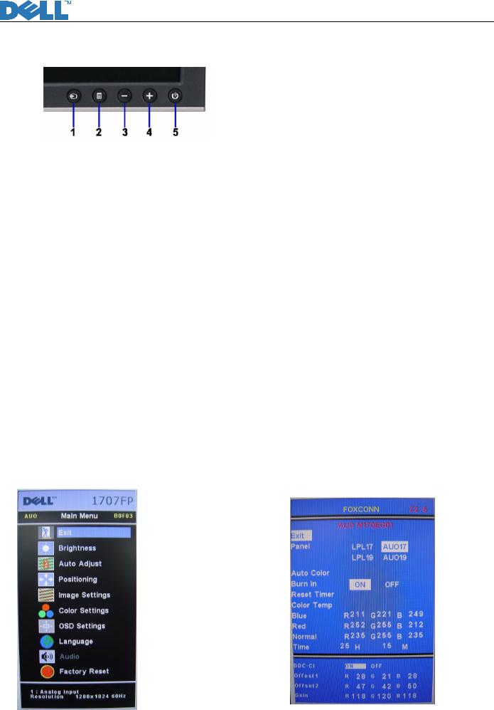
Service Manual
Chapter 5- TEST AND ADJUSTMENT
Function key Definitions
Power Switch with power LED |
Power: On/Off, includes power indicator and Power ICON |
|
indicator |
GreenActive On |
|
|
AmberDPMS |
|
Front Panel Controls |
1- Input select: Select input signal |
|
|
2- Menu: Call out OSD Menu and choose |
|
|
3- (-): symbol molded into button, calls out brightness/Contrast, move |
|
|
down the highlight bar. |
|
|
4-(+)symbol molded into button, move up the highlight bar |
|
|
|
|
Factory Modes Keys Function |
Auto Color Balance |
|
|
Purpose: Automatically calibrate chip ADC parameter by using chip |
|
|
internal DAC. |
|
|
Process: If we want to do “Auto Color Balance” again, please confirm |
|
|
the following steps. |
|
|
1) |
Connect the VGA cable with the standard video pattern generator |
|
|
and display the pattern with blackest and whitest colors. |
|
2) |
Press “Power Key”, to power off the monitor. |
|
3) |
Press “Menu Key” and “Up Key” simultaneously, and then press |
|
|
“Power Key” to power on the monitor. |
|
4) |
Press “Menu Key”, choose “Factory Reset”, then “Factory”. |
|
5) |
Set Burn In Mode item to ON, then execute Auto Color item. |
|
6) |
After the “Auto Color Balance” process finished, go back to |
|
|
“Factory Reset” of Main Menu, and press “All Setting” to exit |
|
|
Factory Menu. |
|
|
|
Factory Mode Introduction
Fig.1 |
Fig.2 |
|
22 |

Service Manual
With signal input, press “Power” button to turn off the monitor. Press “Menu” and “Auto/Plus” buttons together, and then press “Power” button to turn on the monitor. After power on, press “Menu” button to call out Main Menu (Fig.1). Pull down to Factory Reset and enter Factory mode (Fig.2).
AUO M170EG01: Current using panel
Exit : Exit from Factory mode and back to Reset to Factory Settings.
Panel: The current-setting panel is highlighted. “Restart the panel” will be shown with changing to another panel. Auto Color: Automatically calibrate chip ADC parameters by using internal DAC. (Only with Burnin ON) Burn In: Enable or disable the Burn-in mode by choosing ON or OFF.
Reset Timer: Reset the “Turn-on time” of the panel to 0H0M.
Color Temp : The R, G, B of Blue Preset (9300K), Red Preset (5700K) and Normal Preset (6500K) are generated from scaling chip’s back-end white-balance program.
Time : Turn-on time of the panel.
DDC-CI: DDC/CI ON/OFF setting. The DDC/CI shall be defaulted as “ON”.
Please do not change the value of Offset1, Offset2, and Gain; which will be changed with the auto color balance.
Burn-in pattern
If it is a new monitor without VGA cable plugged in, burn-in pattern will selfgenerate automatically. Burnin pattern will not be stopped until plugging in the VGA cable. Then, press “Menu” button to call out OSD Main Menu; pulling down to Factory Reset item and execute All Resetting to disable Bunin ON.
Auto Color Balance (Automatically calibrate chip ADC parameter by using
chip internal DAC.)
5.1If it is a new-built set, press “Auto/Plus” button to execute “Auto Color” at 32gray scale pattern.
5.2Please confirm the following steps to perform “Auto Color Balance”:
-Connect the VGA cable with the standard video pattern generator and display 32gray scale pattern on the monitor.
-Press “Power” button to power off the monitor.
-Press “Menu” and “Auto/Plus” buttons simultaneously; then press “Power” button to power on the monitor.
-Press “Menu” button, pull down to Factory Reset and choose “Factory” item.
-Set Burn In to ON, then execute Auto Color.
-With “Auto Color” finished, return to Reset to Factory Settings OSD and execute All Settings to enable burnin OFF.
23
 Loading...