


R
(with price)
CTK-500
CTK-500
ELECTRONIC KEYBOARD
CONTENTS
Specifications . . . . . . . . . . . . . . . . . . . . . . . . . . . . . . . . . . . . . . . . . . 1
Block Diagram . . . . . . . . . . . . . . . . . . . . . . . . . . . . . . . . . . . . . . . . . 2
Circuit Description . . . . . . . . . . . . . . . . . . . . . . . . . . . . . . . . . . . . . 3
Major Waveforms . . . . . . . . . . . . . . . . . . . . . . . . . . . . . . . . . . . . . . . 7
PCB Views and Major Check Points . . . . . . . . . . . . . . . . . . . . . . . . 8
Schematic Diagrams . . . . . . . . . . . . . . . . . . . . . . . . . . . . . . . . . . . . 9
Troubleshooting . . . . . . . . . . . . . . . . . . . . . . . . . . . . . . . . . . . . . . 11
IC and Transistor Lead Identification . . . . . . . . . . . . . . . . . . . . . 12
Exploded View . . . . . . . . . . . . . . . . . . . . . . . . . . . . . . . . . . . . . . . . 14
Parts List . . . . . . . . . . . . . . . . . . . . . . . . . . . . . . . . . . . . . . . . . . . . . 15
- 2 -
SPECIFICATIONS
General |
|
Number of Keys: |
61 |
Polyphonic: |
16-note |
Preset Tones: |
120 |
Auto-Rhythms: |
40 |
Auto-Accompaniment: |
CASIO Chord/Fingered |
Jukebox Tunes: |
40 |
Chord Memory: |
Real-Time Recording |
|
Memory Capacity: 128 chords (maximum) |
Built-In Speakers: |
12 cm dia. 1.1W Input Rating: 2 pcs. |
Terminals: |
Output Jack [Output Impedance: 50 Ω, Output Voltage: 1.4 V (rms)MAX], |
|
AC Adapter Jack (DC 9 V) |
Auto Power Off: |
Approximately 6 minutes after the last operation |
Power Source: |
2-way AC or DC source |
|
AC: AC adapter |
|
DC: 6 D size dry batteries |
Power Consumption: |
6.7 W |
Dimentions: |
110 x 939 x 337 mm (HWD) |
|
(4-5/16 x 36-15/16 x 13-1/4 inches) (HWD) |
Weight: |
4.5 kg (9.9 lbs) excluding batteries |
Electrical
Current Drain with 9V DC: |
125 mA ± 30% |
No Sound Output |
|
Maximum Volume |
530 mA ± 30% |
with keys C4 to D#5 pressed in Clarinet tone, |
|
Volume; Maximum, Rhythm; Samba, |
|
Tempo; Maximum |
|
Output Level (Vrms with 8 Ω load each channel): |
107 mV ± 30% |
with key C4 pressed in Clarinet tone, |
|
Volume; Maximum |
|
Sound Pressure Level: |
107 dB ± 10 dB |
at 10 cm away from the speaker with key G6 |
|
in Brass-1 tone |
|
Minimum Operating Voltage: |
6.0 V |
— 1 —
— 2 —
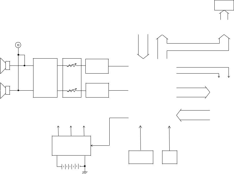
BLOCK DIAGRAM
Output
Main Volume
Control
Filter (R)
T5
Power Amp.
LA4127
IC2
Filter (L)
T6
Speakers
VDD AVDD VCC
Power IC |
|
|
CA5668 |
(APO) |
|
IC1 |
||
|
LEDs
|
|
|
|
|
LED Driver |
|
|
Keys and Switches |
|
|
|
|
|
|
|
IC3 |
|
|
|
|
|
|
|
|
|
|
|
|
|
KI1 ~ KI7 |
|
KO0 ~ KO16 |
|||
|
|
|
|
|
KO0 ~ KO5, KO17 |
|
|
|
|
|
|
ROUT |
|
|
|
CE |
|
|
|
|
|
||
|
|
|
|
OE |
|
|
|
CPU |
|
|
|
|
|
|
|
|
|
LOUT |
|
MSM6626-01 |
|
|
|
|
|
|
A0 ~ A16 |
|
|
|
|
|
|
ROM |
|
|
|
|
|
|
|
|
|
LSI1 |
|
|
MN232000CUQ |
|
|
|
|
|
|
KO18 |
|
|
|
D0 ~ D15 |
LSI2 |
|
|
|
|
||
|
|
|
|
|
|
|
|
|
|
|
|
43.45 MHz Clock
Reset IC
S8053ANO X1
IC4
CIRCUIT DESCRIPTION
Key and Switch Matrix
|
KI0 |
KI1 |
KI2 |
KI3 |
KI4 |
KI5 |
KI6 |
KI7 |
|
|
|
|
|
|
|
|
|
|
|
KO0 |
C2 |
C#2 |
D2 |
D#2 |
E2 |
F2 |
|
|
|
|
|
|
|
|
|
|
|
|
|
KO1 |
F#2 |
G2 |
G#2 |
A2 |
A#2 |
B2 |
|
|
|
|
|
|
|
|
|
|
|
|
|
KO2 |
C3 |
C#3 |
D3 |
D#3 |
E3 |
F3 |
|
|
|
|
|
|
|
|
|
|
|
|
|
KO3 |
F#3 |
G3 |
G#3 |
A3 |
A#3 |
B3 |
|
|
|
|
|
|
|
|
|
|
|
|
|
KO4 |
C4 |
C#4 |
D4 |
D#4 |
E4 |
F4 |
|
|
|
|
|
|
|
|
|
|
|
|
|
KO5 |
F#4 |
G4 |
G#4 |
A4 |
A#4 |
B4 |
|
|
|
|
|
|
|
|
|
|
|
|
|
KO6 |
C5 |
C#5 |
D5 |
D#5 |
E5 |
F5 |
|
|
|
|
|
|
|
|
|
|
|
|
|
KO7 |
F#5 |
G5 |
G#5 |
A5 |
A#5 |
B5 |
|
|
|
|
|
|
|
|
|
|
|
|
|
KO8 |
C6 |
C#6 |
D6 |
D#6 |
E6 |
F6 |
|
|
|
|
|
|
|
|
|
|
|
|
|
KO9 |
F#6 |
G6 |
G#6 |
A6 |
A#6 |
B6 |
|
|
|
|
|
|
|
|
|
|
|
|
|
KO10 |
C7 |
|
|
|
Tempo |
Tempo |
|
|
|
|
|
|
Up |
Down |
|
|
|||
|
|
|
|
|
|
|
|||
|
|
|
|
|
|
|
|
|
|
KO11 |
Power |
Normal |
Fingered |
CASIO |
|
|
|
|
|
Off |
Chord |
|
|
|
|
||||
|
|
|
|
|
|
|
|||
|
|
|
|
|
|
|
|
|
|
|
Accomp. |
Accomp. |
Accomp. |
Accomp. |
Accomp. |
|
|
|
|
KO12 |
Volume 1 |
Volume 5 |
|
|
|
||||
Volume 2 |
Volume 3 |
Volume 4 |
|
|
|
||||
|
(Min) |
(Max) |
|
|
|
||||
|
|
|
|
|
|
|
|||
|
|
|
|
|
|
|
|
|
|
KO13 |
Reverb Off |
Reverb 1 |
Reverb 2 |
|
|
|
|
|
|
|
|
|
|
|
|
|
|
|
|
|
Synchro |
|
Intro/ |
Chord |
Chord |
Ad-Lib |
Jukebox |
Beat |
|
KO14 |
Start/Stop |
Memory |
Memory |
||||||
/ Fill-In |
Ending |
Musician |
Start/Stop |
(Jukebox) |
|||||
|
|
Record |
Play |
||||||
|
|
|
|
|
|
|
|||
|
|
|
|
|
|
|
|
|
|
KO15 |
Bank A |
Bank B |
Bank C |
Bank D |
Bank E |
Bank F |
Bank G |
Bank H |
|
|
|
|
|
|
|
|
|
|
|
KO16 |
Number 1 |
Number 2 |
Number 3 |
Number 4 |
Number 5 |
Solo |
Duo |
Ensenble |
|
Sound |
Sound |
Sound |
|||||||
|
|
|
|
|
|
||||
|
|
|
|
|
|
|
|
|
— 3 —
Nomenclature of Keys
C#2 D#2 |
F#2 G#2 A#2 |
C#3 D#3 |
F#3 G#3 A#3 |
C#4 D#4 |
F#4 G#4 A#4 |
C#5 D#5 |
F#5 G#5 A#5 |
C#6 D#6 |
F#6 G#6 A#6 |
C2 |
D2 |
E2 |
F2 |
G2 |
A2 |
B2 |
C3 |
D3 |
E3 |
F3 |
G3 |
A3 |
B3 |
C4 |
D4 |
E4 |
F4 |
G4 |
A4 |
B4 |
C5 |
D5 |
E5 |
F5 |
G5 |
A5 |
B5 |
C6 |
D6 |
E6 |
F6 |
G6 |
A6 |
B6 |
C7 |
CPU (LSI1: MSM6626-01)
The CPU reads sound data from the ROM in accordance with the pressed key and the selected tone; the CPU can read rhythm data simultaneously when a rhythm pattern is selected. Then it provides the left and the right channels' waveforms separately, by converting the data into the waveforms with two built-in DACs. The CPU also controls keys, switches, and LEDs.
The following table shows the pin functions of LSI1.
Pin No. |
Terminal |
In/Out |
Function |
|||
|
|
|
|
|
|
|
1 ~ 10 |
KO0 ~ KO16 |
Out |
Using time sharing, the terminals provide key and switch |
|||
74 ~ 80 |
scan signals, and LED drive signals. |
|||||
|
|
|
|
|||
|
|
|
|
|
|
|
11 |
KO17 |
Out |
Clock output for the LED driver |
|||
|
|
|
|
|
|
|
12 |
KO18 (APO) |
Out |
APO (Auto Power Off) signal output. |
|||
|
|
|
|
|
|
|
13 |
KO20 |
Out |
Not used. |
|||
|
|
|
|
|
|
|
14 ~ 21 |
KI0 ~ KI7 |
|
In |
Input terminals from the keys and switches |
||
|
|
|
|
|
|
|
22 |
-MI |
|
In |
Power ON trigger pulse input. |
||
|
|
|
|
|
|
|
23 |
-RESET |
|
In |
CPU reset signal input. |
||
|
|
|
|
|
|
|
24 |
REFH |
|
In |
Low level reference voltage input for the built-in DAC |
||
|
|
|
|
|
|
|
25 |
AVDD |
|
In |
+5 V source for the built-in DAC |
||
|
|
|
|
|
|
|
26 |
ROUT |
Out |
Right channel sound signal output |
|||
|
|
|
|
|
|
|
27 |
LOUT |
Out |
Left channel sound signal output |
|||
|
|
|
|
|
|
|
28 |
AGND |
|
In |
Ground (0 V) source for the built-in DAC |
||
|
|
|
|
|
|
|
29 |
REFL |
|
In |
High level reference voltage for the built-in DAC |
||
|
|
|
|
|
|
|
30, 31 |
TEST1, TEST2 |
|
|
|
Not used. Connected to ground. |
|
|
|
|
||||
|
|
|
|
|
|
|
32 |
GND |
|
In |
Ground (0 V) source |
||
|
|
|
|
|
|
|
33, 34 |
COSI, COSO |
In/Out |
43.45 MHz clock input/output |
|||
|
|
|
|
|
|
|
35 |
VDD |
|
In |
+5 V DC source. Regardless of the power switch position, |
||
|
the terminal always receives +5 V DC. |
|||||
|
|
|
|
|
||
|
|
|
|
|
|
|
36 |
-CE |
Out |
Chip enable signal output. Low effective. |
|||
|
|
|
|
|
|
|
37 |
-OE |
Out |
Read enable signal output. Low effective. |
|||
|
|
|
|
|
|
|
38 ~ 40 |
ADR17 ~ ADR19 |
Out |
Not used. |
|||
|
|
|
|
|
|
|
41 ~ 57 |
ADR0 ~ ADR16 |
Out |
Address bus for the ROM |
|||
|
|
|
|
|
|
|
58 ~ 73 |
DIN0 ~ DIN15 |
|
In |
Data bus for the ROM |
||
|
|
|
|
|
|
|
— 4 —

FIlter Block
Since the sound signall from the CPU is a stepped waveform, the filter block is added to smooth the waveform.
To main volume
VDD
2SC3112B
10K 10K 6.2K
1K |
C331J |
C562(H) |
C222(H) |
|
|
|
|
AG |
AG |
|
AG |
From the CPU
Initial Reset Circuit
When batteries are set or an AC adapter is connected, the reset IC provides a low pulse to the CPU. The CPU then initializes its internal circuit.
|
Battery set |
|
|
VDD |
|
Reset IC |
CPU |
|
MSM6626-01 |
||
S8053ANO |
||
LSI1 |
||
IC4 |
||
RESET |
Power On/Off Circuit
When the power switch is turned on, a low level differential pulse is provided to terminal MI of the CPU. Upon receipt of the pulse, the CPU starts the power ON sequence and raises the APO signal to +5 V. When the switch is off, on receiving the KO11 signal at terminal KI0, the CPU drops the APO signal to ground level to shut down power.
VDD |
VDD |
ON |
|
|
|
|
|
||
|
Power Switch |
|
|
|
OFF |
|
MI |
|
|
|
|
|
||
ON |
|
CPU |
KO18 |
|
|
|
|
||
|
KI0 |
MSM6626-01 |
|
|
|
|
APO signal |
||
OFF |
|
|
||
KI1 |
LSI1 |
OFF: 0V |
||
ON |
||||
|
|
ON: +5 V |
||
|
|
|
||
|
KO11 |
|
|
— 5 —
 Loading...