


R
(with price)
CTK-650
CTK-650
ELECTRONIC KEYBOARD
CONTENTS |
|
SPECIFICATIONS .................................................................................................... |
1 |
BLOCK DIAGRAM ................................................................................................... |
2 |
CIRCUIT DESCRIPTION |
|
CPU (HD6433298A16P : H8/329) ..................................................................... |
3 |
DIGITAL SIGNAL PROCESSOR, LSI-S (HG51A115A01FD) .......................... |
4 |
KEY TOUCH LSI (HG52E35P) .......................................................................... |
5 |
POWER AMPLIFIER (LA4598) ......................................................................... |
6 |
BUTTON MATRIX ............................................................................................. |
7 |
KEY MATRIX ..................................................................................................... |
8 |
WIRING DIAGRAM ................................................................................................... |
9 |
IC LEAD IDENTIFICATION AND INTERNAL CIRCUIT .......................................... |
10 |
PCB VIEW AND MAJOR WAVEFORMS ................................................................. |
12 |
SCHEMATIC DIAGRAM ........................................................................................... |
13 |
PARTS LIST ............................................................................................................. |
15 |
EXPLODED VIEW .................................................................................................... |
19 |
SPECIFICATION
Number of keys: |
61 |
|
|
|
Polyphony: |
32-note(max.) |
|
|
|
Preset tones: |
128 |
|
|
|
Magical preset: |
BREAK BEAT |
16 |
MELODYCOMP |
8 |
|
SHADOW DRUM |
4 |
FREE SESSION |
32 |
|
TONE STACK |
40 |
KEY SPLIT |
12 |
|
HYPERACTIVE |
16 |
|
|
Auto-accompaniment: |
Rhythm patterns |
128 |
|
|
|
Tempo |
Adjustable(40 - 255) |
|
|
Chords |
Three system: CASIO CHORD, FINGERD, |
|
|
|
|
FULL-RANGE CHORD |
|
Other |
Variation pattern, fill-in pattern, intro/ending pattern for each |
|
|
|
rhythm. |
|
Song memory: |
song:one |
|
|
|
System:Real-time recording |
||
|
Memory capacity:Up to 1,300 notes |
||
Registration memory: |
4 setups |
|
|
Sound control pads: |
Phrases |
|
10 |
|
Drums |
|
10 |
|
SE/Percussion |
10 |
|
|
Controller |
2 |
|
Digital effects: |
REVERB 1, REVERB 2, REVERB 3, CHORUS, TREMOLO, PHASE |
||
|
SHIFTER, ORGAN SP, ENHANCER, FLANGER, EQLOUNDNESS |
||
DEMO tunes: |
3 tunes |
|
|
Other functions: |
Transpose (F# ~ C ~ F : half-note) |
||
|
Tuning adjustable A4 = 440KHz 50 cents increments |
||
|
Volume control (Main /Accompaniment) |
||
Speakers: |
12cm diameter X 2 (Output:2W+2W) |
||
I/O terminals: |
Power supply |
9V DC jack |
|
|
Headphones |
Stereo mini jack |
|
|
|
|
Output impedance:100 ohm |
|
|
|
Output voltage:4.5V(RMS. max) |
|
Assignable jack |
Standard jack |
|
|
MIDI |
|
IN, OUT |
Power supply: |
3-way AC/DC power sources; |
||
|
Batteries |
Six D-size |
|
|
Battry life |
Approximately 5 hours on R20P(SUM-1) |
|
|
AC |
|
Required optional AD-5 AC adaptor |
|
Car battery |
Required optional CA-5 car adaptor |
|
Auto power off: |
Approximately 6 minutes after the last operation |
||
Power consumption: |
7.7W |
|
|
Dimensions: |
942 X 367 X 135 mm(HWD) |
||
|
31 7/16" X 14 1/2" X 4 3/8" inches(HWD) |
||
Weight: |
5.2kg(11.7lbs) excluding batteries |
||
Accessory: |
Score stand |
|
|
— 1 —
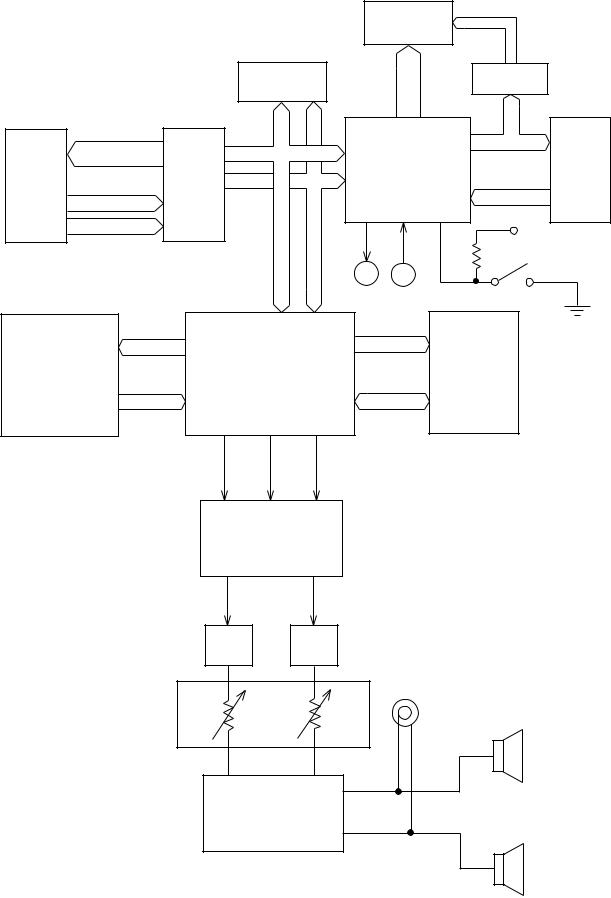
BLOCK DIAGRAM |
|
|
7-Segment |
LO0~LO4 |
|
||
|
|
|
|
LED |
|
|
|
|
|
|
|
|
|
|
|
|
|
RAM-1(64K) |
|
La |
|
LED driver |
|
|
|
MN4464-08L-1 |
|
~Lp |
|
BA612 |
|
|
|
|
|
|
|
KO0~4 |
|
KC0~KC7 |
Key Touch |
D0~D7 |
|
CPU |
|
KO0~KO5 |
|
|
|
|
|
||||
LSI |
|
|
|
|
|
||
|
|
HD6433298A16P |
Buttons |
||||
|
|
Address Bus |
|||||
Keyboard |
|
|
|||||
|
|
(H8/329) |
|
|
|
||
|
|
|
|
KI1~KI7 |
|
||
|
HG52E35P |
|
|
|
|
||
SI0~SI7 |
|
|
|
|
|
||
FI0~FI7 |
|
|
|
|
|
VDD |
|
|
|
|
|
|
|
|
|
|
|
|
MIDI |
|
100K |
|
|
|
|
|
OUT |
IN |
|
Power Switch |
|
RA0~RA19 |
LSI-S |
EA0~EA12 |
|
RAM-2(64K) |
|
||
ROM(16M) |
|
|
|
|
|
|
|
TC5316200CP-C079 |
|
HG51A115A01FD |
|
|
MN4464-08L-2 |
|
|
|
|
|
|
|
|
||
RD0~RD15 |
|
ED0~ED7 |
|
|
|
||
WCK1 SLOP BCK
D/A Converter
µPD6376CX
Filter Filter
Main |
Output |
|
Volume |
||
|
Power Amplifier
Speakers
LA4598
— 2 —
CIRCUIT DESCRIPTION
CPU(HD6433298A16P : H8/329)
The 16-bit CPU contains a 32K-byte ROM, a 1K-byte RAM, an 8-bit A/D converter, timers and I/O ports. The CPU accesses to the DSP, Key Touch LSI, RAM, buttons and LEDs. But the CPU directly receives MIDI and pedal signals.
Pin No. |
Terminal |
In/Out |
|
|
|
|
|
Function |
|
1 |
P40/IRQ2 |
In |
KO signal data. |
||||||
2 |
P41/IRQ1 |
In |
Timing signal for KO signal. |
||||||
3 |
P42/IRQ0 |
In |
APO signal output. |
||||||
4 |
P43/-RD |
Out |
Read signal outpt. |
||||||
5 |
P44/-WR |
Out |
Write signal output. |
||||||
7 |
P46/PHI |
Out |
System clock output. |
||||||
8 |
P47/-WAIT |
In |
Wait signal input |
||||||
9 |
P50/Txd |
Out |
MIDI signal output. |
||||||
10 |
P51/Rxd |
In |
MII signal input. |
||||||
11 |
P52/SCK |
Out |
Reset signal output. |
||||||
12 |
-RESET |
In |
Reset signal input. |
||||||
13 |
-NMI |
In |
Power on signal input.(Low active) |
||||||
14 |
Vcc |
In |
+5V source. |
|
|
||||
15 |
-STBY |
In |
Standby signal input. Connected to +5V. |
||||||
16 |
Vss |
In |
Ground(0V) source. |
||||||
17,18 |
XTAL,EXTAL |
In/Out |
20MHz clock pulse input/output. Connected to crystal. |
||||||
19,20 |
MD1,MD0 |
In |
Selection for system. |
||||||
|
|
|
|
|
|
|
|
|
|
|
|
|
|
MD1 |
MD0 |
|
MODE |
|
|
|
|
|
|
0 |
|
1 |
|
MODE-1 : Internal ROM mode |
|
|
|
|
|
1 |
|
0 |
|
MODE-2 : Non internal ROM mode |
|
|
|
|
|
1 |
|
1 |
|
MODE-3 : Single chip mode |
|
|
|
|
|
|
|
|
|
||
21 |
AVss |
In |
Analog ground source. |
||||||
22 |
P70/AN0 |
In |
Connected to ground. |
||||||
23~29 |
P71/AN0~P77/AN7 |
In |
KI signal input. |
||||||
30 |
AVcc |
In |
+5V source. |
|
|
||||
31~38 |
P60/FTCI~P67/TMO1 |
Out |
Control signal for 7-segment LED. |
||||||
39 |
Vcc |
In |
+5V source. |
|
|
||||
41~56 |
P26/A14~P10/A0 |
Out |
Address bus. |
|
|
||||
48 |
Vss |
In |
Ground(0V) source. |
||||||
57~64 |
P30/D0~P37/D7 |
In/Out |
Data bus. |
|
|
|
|
||
— 3 —
DIGITAL SIGNAL PROCESSOR, LSI-S (HG51A115A01FD)
The LSI-S is a 16-bit DSP(Digital Signal Processor) and accessable to 16M-bit sound source ROM and to 64Kbit RAM. The DSP can read data of 32 polyphonic note from the ROM and provides two 16-bit serial dat with timing signals to each channel's D/A converter.
Pin No. |
Terminal |
In/Out |
Function |
|
1~7 |
D7~D0 |
I/O |
Data bus. |
|
11 |
GND7 |
In |
Ground(0V) source. |
|
12 |
CK16 |
Out |
16.384MHz clock pulse output. |
|
13 |
VCC6 |
In |
+5V source |
|
14 |
CK0 |
In |
Clock pulse input. Connected to terinal CK16. |
|
16 |
VCC1 |
In |
+5V source. |
|
17 |
GND1 |
In |
Ground(0V) source. |
|
18,19 |
XTI, XTO |
In/Out |
16.384MHz clock pulse input/output. Connected to crystal. |
|
21 |
CCSB |
I |
Chip select signal input. |
|
22~25 |
CA0~CA3 |
In |
Address bus. |
|
26 |
CE0 |
In |
Connected to ground.(ROM interface ontrol terminal) |
|
27 |
CWRB |
In |
Write enable signal. |
|
28 |
CRDB |
In |
Read enebla signal. |
|
33 |
RESB |
In |
Reset sna iput |
|
34 |
TESB |
In |
Connected to +5V. |
|
40~49 |
RD0~RD15 |
In |
Data bus for sound source ROM. |
|
52~57 |
||||
|
|
|
||
50 |
VCC2 |
In |
+5V source. |
|
51 |
GND2 |
In |
Ground(0V) source. |
|
59 |
RA22 |
Out |
Chip enable signal output for ROM. |
|
62~73 |
RA0~RA19 |
Out |
Address bus for sound source ROM. |
|
75~82 |
||||
|
|
|
||
74 |
GND5 |
In |
Ground(0V) source. |
|
84 |
VCC3 |
In |
+5V source. |
|
85 |
GND3 |
In |
Ground source. |
|
86 |
WOK1 |
Out |
Ward clock for DAC. |
|
88 |
SOLP |
Out |
16-bit serial data for L-channel DAC. |
|
89 |
BOK |
Out |
Bit clock for DAC. |
|
93 |
VCC5 |
In |
+5V source. |
|
95,97 |
|
|
|
|
99~105 |
EA0~EA12 |
Out |
Address bus for RAM. |
|
107,109 |
||||
|
|
|
||
110,112 |
|
|
|
|
|
|
|
|
|
96 |
EWEB |
Out |
Write enable signal for RAM. |
|
106 |
EOEB |
Out |
Read enable signal for RAM. |
|
108 |
VCC7 |
In |
+5V source. |
|
111 |
ECEB |
Out |
Chip eneble signal for RAM. |
|
118 |
VCC4 |
In |
+5V source. |
|
119 |
GND4 |
In |
Ground(0V) source. |
|
123~130 |
ED0~ED7 |
In/Out |
Data bus for RAM. |
|
131 |
GND6 |
In |
Connected to Ground. |
|
132 |
SSI |
In |
Connected to Ground. |
|
133 |
SBCK |
In |
Connected to Ground. |
|
134 |
SWCK |
In |
Connected to Ground. |
— 4 —
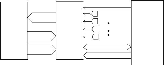
KEY TOUCH LSI(HG52E35P)
By counting the time between the first key input signal FI and the second SI from the keyboard unit, the key touch LSI detects key velocity of 256-step. Then the LSI sends the CPU note numbers and their velocities.
|
|
|
Key Touch LSI |
|
|
|
|
CPU |
|
|
|
HG52E35P |
|
|
|
|
HD6433298A16P |
|
|
|
RESB |
|
|
|
|
P52/SCK |
|
|
|
CCSB |
|
|
|
|
A12 |
|
|
|
|
|
|
|
A14 |
|
|
|
KC0~KC7 |
|
|
|
|
||
|
|
|
|
|
|
P44/-WR |
||
|
|
|
CWRB |
|
|
|
|
|
|
|
|
|
|
|
|
P42/IRQ0 |
|
|
|
|
|
|
|
|
|
|
|
Keyboard |
|
CRDB |
|
|
|
|
P43/-RD |
|
|
|
|
|
|
|||
|
|
|
|
|
|
|
||
|
|
FI0~FI9 |
CKI |
|
|
|
|
P46/PHI |
|
|
|
|
|
|
|||
|
|
|
|
|
|
|
||
|
|
SI0~SI9 |
P30/D0~P37/D7 |
|
D0~D7 |
|
CD0~CD7 |
|
|
|
|
|
|
|
|
|
|
|
|
|
P12/A2~P10/A0 |
|
A0~A2 |
|
CA0~CA2 |
|
|
|
|
|
|
|
|
|
|
Pin No. |
Terminal |
In/Out |
|
|
Function |
|
|
|
1 |
REQB |
Out |
Interrupt request. Not used. |
|
|
|
|
|
2,3 |
FI10,SI10 |
In |
Connected to +5V. |
|
|
|
|
|
4 |
VCC |
In |
+5V source. |
|
|
|
|
|
5 |
CRDB |
In |
Read enable signal. |
|
|
|
|
|
6 |
CWRB |
In |
Write enable signal. |
|
|
|
|
|
7 |
CCBB |
In |
Chip select signal. |
|
|
|
|
|
8 |
T |
In |
Test terminal. Connected to +5V. |
|
|
|||
9 |
STYB |
In |
Standby terminal. Connected to +5V. |
|
|
|||
10 |
RESB |
In |
Reset signal. |
|
|
|
|
|
11 |
W |
In |
Test terminal. Connected to +5V. |
|
|
|||
12 |
CKI |
In |
External clock input. |
|
|
|
|
|
13 |
TMD |
In |
Test terminal. Connected to ground. |
|
|
|||
14 |
TST |
In |
Test terminal. Connected to ground. |
|
|
|||
15 |
CKO |
Out |
External clock output. Not used. |
|
|
|||
16 |
GND |
In |
Ground(0V) source. |
|
|
|
|
|
17 |
XIN |
In |
Clock pulse input. Connected to ground. |
|
|
|||
18 |
XOUT |
Out |
Clock pulse output. Not used. |
|
|
|||
19 |
TRES |
In |
Test terminal. Connected to ground. |
|
|
|||
20~28 |
CD0~CD7 |
In/Out |
Data bus. |
|
|
|
|
|
24 |
GND |
In |
Ground(0V) source. |
|
|
|
|
|
29~31 |
CA0~CA2 |
Out |
Address bus. |
|
|
|
|
|
32 |
VCC |
In |
+5V source. |
|
|
|
|
|
33~43 |
FI0~FI9 |
|
|
|
|
|
|
|
53~55 |
In |
Key input signal. |
|
|
|
|
|
|
SI0~SI9 |
|
|
|
|
|
|||
57~63 |
|
|
|
|
|
|
|
|
|
|
|
|
|
|
|
|
|
40 |
VCC |
In |
+5V source. |
|
|
|
|
|
44~53 |
KC0~KC7 |
Out |
Key scan signal. |
|
|
|
|
|
48,56 |
GND |
In |
Ground(0V) source. |
|
|
|
|
|
54 |
VCC |
In |
+5V source. |
|
|
|
|
|
— 5 —
 Loading...