


 Loading...
STAGEPAS 500
SERVICE MANUAL
Speaker |
Mixer |
Speaker |
CONTENTS |
|
SPECIFICATIONS ............................................... |
3 |
PANEL LAYOUT .................................. |
4 |
DIMENSIONS ......................................................... |
4 |
CIRCUIT BOARD LAYOUT .............. |
5 |
DISASSEMBLY PROCEDURE ........................... |
6 |
LSI PIN DESCRIPTION LSI ............................ |
16 |
IC BLOCK DIAGRAM IC ................................. |
18 |
CIRCUIT BOARDS ..................................... |
19 |
INSPECTIONS ......................................................... |
27 |
ADJUSTMENT OF AMPLIFIER UNIT |
|
..................................................... |
30 |
FACTORY SETTING .................................. |
30 |
TROUBLE SHOOTING ............ |
31 |
PARTS LIST |
|
BLOCK DIAGRAM |
|
CIRCUIT DIAGRAM |
|
PA 011840
200612-155400
HAMAMATSU, JAPAN 1
Copyright (c) Yamaha Corporation. All rights reserved. PDF 
 ’07.01

STAGEPAS 500
IMPORTANT NOTICE
This manual has been provided for the use of authorized Yamaha Retailers and their service personnel. It has been assumed that basic service procedures inherent to the industry, and more specifically Yamaha Products, are already known and understood by the users, and have therefore not been restated.
WARNING :
Failure to follow appropriate service and safety procedures when servicing this product may result in personal injury, destruction of expensive components and failure of the product to perform as specified. For these reasons, we advise all Yamaha product owners that all service required should be performed by an authorized Yamaha Retailer or the appointed service representative.
IMPORTANT :
This presentation or sale of this manual to any individual or firm does not constitute authorization certification, recognition of any applicable technical capabilities, or establish a principal-agent relationship of any form.
The data provided is belived to be accurate and applicable to the unit(s) indicated on the cover. The research engineering, and service departments of Yamaha are continually striving to improve Yamaha products. Modifications are, therefore, inevitable and changes in specification are subject to change without notice or obligation to retrofit. Should any discrepancy appear to exist, please contact the distributor’s Service Division.
WARNING :
IMPORTANT :
Static discharges can destroy expensive components. Discharge any static electricity your body may have accumulated by grounding yourself to the ground bus in the unit (heavy gauge black wires connect to this bus.)
Turn the unit OFF during disassembly and parts replacement. Recheck all work before you apply power to the unit.
WARNING: CHEMICAL CONTENT NOTICE!
The solder used in the production of this product contains LEAD. In addition, other electrical/electronic and/or plastic (Where applicable) components may also contain traces of chemicals found by the California Health and Welfare Agency (and possibly other entities) to cause cancer and/or birth defects or other reproductive harm.
DO NOT PLACE SOLDER, ELECTRICAL/ELECTRONIC OR PLASTIC COMPONENTS IN YOUR MOUTH FOR ANY REASON WHAT SO EVER!
Avoid prolonged, unprotected contact between solder and your skin! When soldering, do not inhale solder fumes or expose eyes to solder/ flux vapor!
If you come in contact with solder or components located inside the enclosure of this product, wash your hands before handling food.
IMPORTANT NOTICE FOR THE UNITED KINGDOM
Connecting the Plug and Cord
WARNING: THIS APPARATUS MUST BE EARTHED
IMPORTANT. The wires in this mains lead are coloured in accordance with the following code:
GREEN-AND-YELLOW BLUE
BROWN
As the colours of the wires in the mains lead of this apparatus may not correspond with the coloured markings identifying the terminals in your plug proceed as follows:
The wire which is coloured GREEN-and-YELLOW must be connected to the terminal in the plug which is marked by the letter E or by the safety earth symbol  or colored GREEN or GREEN-and-YELLOW.
The wire which is coloured BLUE must be connected to the terminal which is marked with the letter N or coloured BLACK.
The wire which is coloured BROWN must be connected to the terminal which is marked with the letter L or coloured RED.
 WARNING
Components having special characteristics are marked  and must be replaced with parts having specification equal to those originally installed.

2
 SPECIFICATIONS
 General Specifications
Maximum Output Power
250 W+250 W (± 10 %)/4 Ω @10 % THD at 1 kHz (SPEAKER L/R)  200 W+200 W/4 Ω @1 % THD at 1 kHz (SPEAKER L/R)
Maximum Output Level
116 dB (1 m)
Frequency Response (Nominal output level @ 1 kHz)
-3 dB, 0 dB, +1 dB @20 Hz–20 kHz (MUSIC/SPEECH=MUSIC) (MONITOR OUT)
-3 dB, 0 dB, +1 dB @80 Hz–20 kHz (MUSIC/SPEECH=SPEECH) (REC OUT)
-3 dB, 0 dB, +1 dB @20 Hz–20 kHz, 1 W Output (MUSIC/SPEECH=MUSIC, without Speaker EQ)
(SPEAKERS L/R)
Total Harmonic Distortion
 0.5 % @20 Hz, 1 kHz, 20 kHz, +14 dBu GAIN=nominal
(MONITOR OUT, REC OUT)
Hum & Noise (Equivalent Input Noise, Rs=150 Ω , MIC/LINE=MIC)
 -106 dBu (CH1/2)
 -112 dBu (CH3/4)
 -65 dBu Residual output noise (SPEAKERS L/R)
Crosstalk (1 kHz)
 -70 dB between input channels
Phantom Voltage
+15 V (CH1–4)
LIMIT/COMP switch
ON=Comp, OFF=Limit (CH1/2)
Power Consumption
65 W
Weight
24 kg (Speaker x 2 + Powered Mixer)
Stereo Input Channel Equalization
± 15 dB |
|
HIGH |
10 kHz shelving |
LOW |
100 Hz shelving |
Accessories
Power Cable, Speaker Cable, Owner’s Manual
Option
Microphone
 Speakers (500S)
Enclosure
2 way bass-reflex type, Polypropylene, Black
Crossover Frequency
4.0 kHz (LF: 12 dB/oct, HF: 12 dB/oct)
Frequency Range
55 Hz–20 kHz (-10 dB)
Speaker Unit
LF: 10" (25 cm) Cone
HF: 1" (2.54 cm) Compression Driver
STAGEPAS 500


250W+250W(±10%)/4Ω @10% THD at 1kHz (SPEAKERS L/R)200W+200W/4Ω @1% THD at 1kHz (SPEAKERS L/R)
116dB ( 1m)
( @1kHz)
-3dB, 0dB, +1dB @20Hz 20kHz (MUSIC/SPEECH=MUSIC) (MONITOR OUT)
-3dB, 0dB, +1dB @80Hz 20kHz (MUSIC/SPEECH=SPEECH) (REC OUT)
-3dB, 0dB, +1dB @20Hz 20kHz, 1W (MUSIC/SPEECH=MUSIC, EQ )
(SPEAKERS L/R)
0.5% @20Hz, 1kHz, 20kHz +14dBu GAIN= (MONITOR OUT, REC OUT)
& ( , Rs=150Ω, MIC/LINE =MIC)
-106dBu (CH1/2)-112dBu (CH3/4)
-65dBu (SPEAKERS L/R)
(1 kHz)
-70 dB
+15V (CH1-4)
LIMIT/COMP
ON= , OFF= (CH1/2)
65 W
24 kg ( 2 )
(±15 dB)
HIGH: 10kHz LOW: 100Hz
 (500S)
2-way , ,
4.0kHz (LF:12dB/oct, HF:12dB/oct)
55Hz 20kHz (-10dB)
LF: 10" (25 cm)
HF: 1" (2.54 cm)
3
STAGEPAS 500
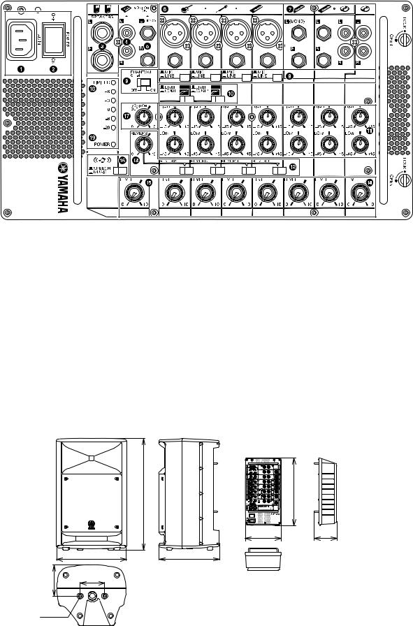
 PANEL LAYOUT
MASTER |
1 |
2 |
3 |
4 |
5/6 |
7/8 |
9/10 |
|
q [AC IN] jack ([AC IN] ) |
|
|
!0[LIMIT/COMP] switches |
([LIMIT/COMP] ) |
||||
w [POWER] switch ([POWER] ) |
|
|
!1Equalizer [HIGH]/[LOW] |
(EQ( )) |
||||
e [SPEAKERS L/R] jacks (for included speakers (500S) only) |
|
!2[REVERB] switches ([REVERB] ) |
||||||
([SPEAKERS L/R] ( (500S) )) |
|
!3[REVERB] control ([REVERB] ) |
||||||
r [REC OUT L/R] jacks ([REC OUT L/R] ) |
|
|
!4[LEVEL] controls |
([LEVEL] ) |
||||
t [MONITOR OUT L(MONO)/R] jacks |
|
|
!5[MASTER LEVEL] control |
|
||||
([MONITOR OUT L(MONO)/R] ) |
|
|
|
([MASTER LEVEL] ) |
||||
y Channel input jacks (CH 1 to 4) |
|
|
!6[SPEECH/MUSIC] switch |
|
||||
( (CH 1 4)) |
|
|
|
([SPEECH/MUSIC] ) |
|
|||
u Stereo channel input jacks (CH 5/6, 7/8, 9/10) |
|
|
!7[MONITOR OUT] control |
|
|
|||
( (CH 5/6 7/8 9/10)) |
|
|
([MONITOR OUT] ) |
|||||
i [MIC/LINE] switches ([MIC/LINE] ) |
|
|
!8[LEVEL] meter ([LEVEL] ) |
|||||
o [PHANTOM] switch ([PHANTOM] ) |
|
!9[POWER] indicator ([POWER] ) |
||||||
 DIMENSIONS
Speaker
152
2-M8 x 25
Mixer

 7/8 9/10
5/6 |
|
4 |
|
|
3 |
|
544.5 |
MASTER 1 2 |
330 |
175 |
111.5 |
342 |
298 |
120
Unit: mm
4
STAGEPAS 500
 CIRCUIT BOARD LAYOUT
Front view |
|
Right side view |
|||||
|
|
Speaker HF <Tweeter> |
|
|
|
||
NETWORK |
|
HF < > |
|
|
|
||
|
|
|
POWER |
||||
|
|
|
|
|
|
|
|
|
|
|
|
|
|
|
|
|
|
|
NETWORK |
|
DSP |
|
|
CONTROL1 (1/3)
CONTROL2 (2/3)
CONTROL3 (3/3)
AMP

 JACK
JACK
Speaker LF <Woofer>
LF < >
 Rear view
CONTROL1 (1/3) |
|
POWER |
|
CONTROL2 (2/3) |
|
|
|
|
|
DSP
CONTROL3 (3/3)
AMP
JACK
5
STAGEPAS 500
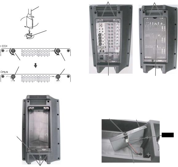
 DISASSEMBLY PROCEDURE
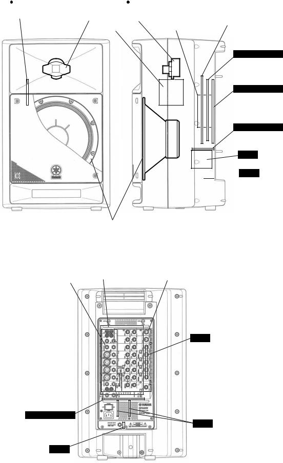
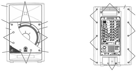
1. |
Front Grille Assembly |
1. |
|
Ass'y 1 |
|||
|
(Time required: About 1 minute) |
1-1 |
[190] 4 Ass'y |
||||
1-1 |
Remove the four (4) screws marked [190]. The front |
|
|
1 |
|
||
|
grille assembly can then be removed. (Fig. 1) |
2. LF 2 |
|||||
2. |
Speaker LF (Woofer) |
||||||
2-1 Ass'y 1 |
|||||||
|
(Time required: About 2 minutes) |
2-2 [170A] 8 LF |
|||||
2-1 |
Remove the front grille assembly. (See procedure 1) |
|
|
1 |
|
||
2-2 |
Remove the eight (8) screws marked [170A]. The |
2-3 |
LF |
||||
|
speaker LF (woofer) can then be removed. (Fig. 1) |
|
|
LF 1 |
|||
2-3 |
Remove the wire LF (red/black) attached to the |
3. |
|
|
|||
|
speaker LF (woofer). (Photo 1) |
|
|||||
3. |
Front Cabinet Unit, Rear Cabinet Unit |
|
|
2 |
|||
3-1 |
[150A] 14 |
||||||
|
(Time required: About 2 minutes) |
|
|
1 2 |
|||
3-1 Remove the fourteen (14) screws marked [150A]. |
3-2 |
LF |
|||||
|
The front cabinet unit and rear cabinet unit can then |
|
|
LF 1 |
|||
|
be separated. (Fig. 1, Fig. 2) |
3-3 |
HF |
||||
3-2 |
Remove the wire LF (red/black) attached to the |
|
|
HF 2 |
|||
|
speaker LF (woofer). (Photo 1) |
|
|
|
|||
3-3 Remove the wire HF (yellow/blue) attached to the |
|
|
LF |
||||
|
speaker HF (tweeter). (Photo 2) |
|
|
HF |
|||
* |
Take care not to open the front cabinet unit and |
|
|
|
|
||
|
rear cabinet unit too wide or the speaker LF |
|
|
|
|
||
|
(woofer) terminal and speaker HF (tweeter) |
|
|
|
|
||
|
terminal may be damaged. |
|
|
|
|
||
<Front view> |
[170A] |
<Rear view> |
Rear cabinet unit |
||||
|
|
|
|
|
[150A] |
( ) |
|
Front cabinet unit |
|
|
|
|
|||
|
|
|
|
|
|||
( ) |
|
|
|
|
|
||
|
|
|
|
|
[150A] |
[150A] |
|
|
|
|
|
|
|
||
|
[190] |
[190] |
|
|
|
|
|
|
|
|
|
|
|
||
Front grille assembly |
Speaker LF (Woofer) |
|
|
|
|||
( Ass'y) |
|
|
|
||||
( LF ( )) |
|
[150A] |
|||||
|
|
|
|||||
|
[170A] |
[170A] |
|
|
|
|
|
|
|
|
|
|
[150A] |
|
|
|
[190] |
[190] |
|
|
|
|
|
|
|
|
|
|
[150A] |
[150A] |
|
|
|
|
|
|
|
||
|
|
[170A] |
|
|
|
|
|
|
|
|
|
|
[150A] |
|
|
[170A]: Bind Head Tapping Screw-P P BIND |
|
[150A]: Bind Head Tapping Screw-A A BIND |
|||||
|
5.0X18 BL CR3 (WJ559700) |
|
|
5.0X45 NI-BL (WJ329900) |
|
||
[190]: |
Bind Head Tapping Screw-P P BIND |
|
|
Fig.2 ( 2) |
|
||
|
4.0X12 NI-BL (WJ329500) |
|
|
|
|||
Fig.1 ( 1)
6
|
Speaker LF (Woofer) |
|
( LF( )) |
Wire LF (Red) |
Wire LF (Black) |
( LF( )) |
( LF( )) |
Photo 1 ( 1)
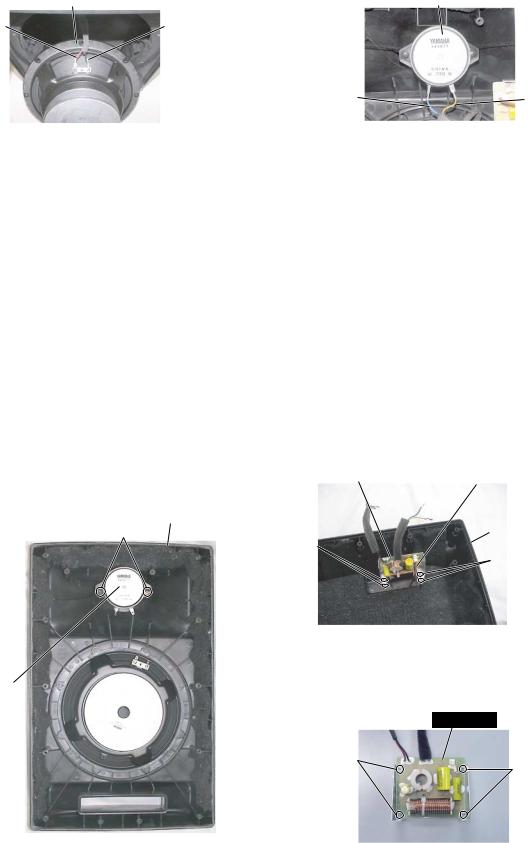
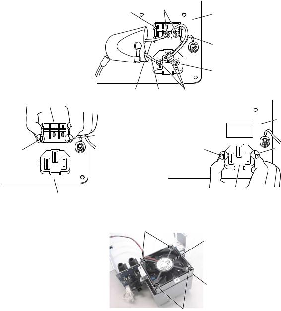
4.Speaker HF (Tweeter)
(Time required: About 3 minutes)
4-1 Separate the front cabinet unit and rear cabinet unit. (See procedure 3)
4-2 Remove the two (2) screws marked [140]. The speaker HF (tweeter) can then be removed from the front cabinet unit. (Photo 3)
5.Network Assembly, NETWORK Circuit
Board (Time required: About 4 minutes)
5-1 Separate the front cabinet unit and rear cabinet unit. (See procedure 3)
5-2 Remove the SP connector assembly from the network assembly. (Photo 4)
5-3 Remove the four (4) screws marked [30]. The network assembly can then be removed from the rear cabinet unit. (Photo 4)
5-4 Remove the four (4) screws marked [N40]. The NETWORK circuit board can then be removed. (Photo 4-1)
<Rear view> |
Front cabinet unit |
|
( ) |
|
[140] |
Speaker HF (Tweeter)
( HF ( ))
[140]: Bind Head Tapping Screw-B B BIND 4.0X20 NI-BL (WJ329100)
Photo 3 ( 3)
STAGEPAS 500
Speaker HF (Tweeter)
( HF( ))
Wire HF (Blue) |
Wire HF (Yellow) |
( HF( )) |
( HF( )) |
Photo 2 ( 2)
4.HF 3
4-1 3
4-2 [140] 2HF 3
5.Ass'y NETWORK
4
5-1 3
5-2 Ass'y SP
4 5-3 [30] 4
Ass'y 4
5-4 [N40] 4 NETWORK4-1
Network assembly |
SP connector assembly |
( Ass'y) |
(SP ) |
Rear cabinet unit ( )
[30]
[30]
[30]: Bind Head Tapping Screw-B B BIND 3.0X10 NI-BL (WJ329200)
Photo 4 ( 4)
● Network Assembly Ass’y
NETWORK
[N40]
[N40]
[N40]: Pan Head Tapping Screw-B B PAN 3.0X8 CR3 (WJ329000)
Photo 4-1 ( 4-1)
7
STAGEPAS 500
6.Mixer Assembly, Cover Mold Assembly
(Time required: About 1 minute)
6-1 Rotate the two (2) straight slots on the fastener heads with a coin driver or minus driver until each straight slot is in alignment with the “OPEN” position. The mixer assembly or cover mold assembly can then be removed. (Photo 5)
7.JACK Circuit Board
(Time required: About 1 minute)
7-1 Remove the mixer assembly or cover mold assembly. (See procedure 6)
7-2 Remove the three (3) screws marked [50A]. The mount bracket assembly can then be removed together with the JACK circuit board. (Photo 6)
7-3 Remove the SP connector assembly from the JACK circuit board. (Photo 6-1)
7-4 Remove the hexagonal nut marked [210a]. The JACK circuit board can then be removed from the mount bracket assembly. (Photo 6-1)
Coin driver or minus driver ( )
Fastner head ( )
Fastner head |
Fastner head |
|
( ) |
||
( ) |
||
|
Mount bracket assembly ( Ass'y)
[50A]
[50A]: Bind Head Tapping Screw-P P BIND 4.0X12 NI-BL (WJ329500)
Photo 6 ( 6)
6.Ass'y Ass'y
1
6-1 2 “OPEN” Ass'yAss'y 5
7.JACK 1
7-1 Ass'y Ass'y6
7-2 [50A] 3 JACKAss'y 6
7-3 JACK SP 6-1 7-4 [210a] 1Ass'y JACK
6-1
Fastner head |
Fastner head |
( ) |
( ) |
Mixer assembly |
Cover mold assembly |
|
( Ass'y) |
||
( Ass'y) |
||
|
Photo 5 ( 5)
Mount bracket assembly [210a] ( Ass'y)
JACK
SP connector assembly (SP )
[210a]: Hexagonal Nut M15.0 BL
Photo 6-1 ( 6-1)
8
|
|
|
|
STAGEPAS 500 |
8. |
Rear Case |
8. 2 |
||
|
(Time required: About 2 minutes) |
8-1 Ass'y 6 |
||
8-1 |
Remove the mixer assembly. (See procedure 6) |
8-2 |
[400] 8 Ass'y |
|
8-2 |
Remove the eight (8) screws marked [400].The rear |
|
|
7 |
|
case can then be removed from the mixer assembly. |
|
|
|
|
(Photo 7) |
|
|
|
9. |
Shield Bracket 2 |
9. |
|
2 2 |
|
(Time required: About 2 minutes) |
9-1 Ass'y 6 |
||
9-1 |
Remove the mixer assembly. (See procedure 6) |
9-2 |
|
8 |
9-2 |
Remove the rear case. (See procedure 8) |
9-3 |
[380] 4 2 |
|
9-3 |
Remove the four (4) screws marked [380]. The |
|
|
8 |
|
shield bracket 2 can then be removed. (Photo 8) |
|
|
|
10. |
POWER Circuit Board |
10. |
POWER 3 |
|
|
(Time required: About 3 minutes) |
10-1 Ass'y 6 |
||
10-1 Remove the mixer assembly. (See procedure 6) |
10-2 8 |
|||
10-2 Remove the rear case. (See procedure 8) |
10-3 2 9 |
|||
10-3 Remove the shield bracket 2. (See procedure 9) |
10-4 [290] 6 POWER |
|||
10-4 Remove the six (6) screws marked [290].The POWER |
|
|
9 |
|
|
circuit board can then be removed. (Photo 9) |
|
|
|
● Mixer Assembly Ass’y
Shield bracket 2 ( 2)
[400]
[380]
[380]
Rear case ( ) [400]
[400]: Hexagonal Tapping Screw-B B 3.0X8 NI-BL (AAX62010)
Photo 7 ( 7)
[380]: Bind Head Tapping Screw-B B BIND 3.0X8 CR3 (AAX61980)
Photo 8 ( 8)
[290]
POWER
[290]
[290]: Pan Head Tapping Screw-B B PAN 3.0X8 CR3 (WJ329000)
Photo 9 ( 9)
9

STAGEPAS 500
11. |
DSP Circuit Board |
11. |
DSP 2 |
|
(Time required: About 2 minutes) |
11-1 Ass'y 6 |
|
11-1 Remove the mixer assembly. (See procedure 6) |
11-2 |
8 |
|
11-2 |
Remove the rear case. (See procedure 8) |
11-3 |
2 9 |
11-3 |
Remove the shield bracket 2. (See procedure 9) |
11-4 |
CONTROL2 (2/3) CN27 CN33 |
11-4 |
Remove the DSP circuit board from the connectors |
|
DSP 10 |
|
CN27 and CN33 of the CONTROL2 (2/3) circuit |
|
|
|
board. (Photo 10) |
|
|
CONTROL2 (2/3) [CN32]
[CN33]
DSP
[CN27]
[CN28]
Photo 10 ( 10)
12. |
AMP Circuit Board, CONTROL3 (3/3) |
12. |
AMP CONTROL3 (3/3) |
||||
|
Circuit Board (Time required: About 4 minutes) |
|
4 |
||||
12-1 Remove the mixer assembly. (See procedure 6) |
12-1 Ass'y 6 |
||||||
12-2 Remove the rear case. (See procedure 8) |
12-2 8 |
||||||
12-3 Remove the shield bracket 2. (See procedure 9) |
12-3 2 9 |
||||||
12-4 |
Remove the two (2) hexagonal nuts marked [240aA] |
12-4 |
[240aA] 2 |
||||
|
from the panel printing side. (Photo 11) |
|
11 |
||||
12-5 |
Remove the two (2) screws marked [270]. The |
12-5 |
[ 2 7 0 ] 2 |
A M P |
|||
|
phone bracket can then be removed together with |
|
CONTROL3 (3/3) |
||||
|
the AMP circuit board and CONTROL3 (3/3) circuit |
|
12 |
||||
|
board. (Photo 12) |
12-6 |
[260A] 2 |
||||
12-6 |
Remove the two (2) screws marked [260A]. The |
|
AMP CONTROL3 (3/3) |
||||
|
AMP circuit board and CONTROL3 (3/3) circuit |
|
13 |
|
|
|
|
|
board can then be removed from the phone bracket. |
12-7 |
[260B] 1 CONTROL3 (3/3) |
||||
|
(Photo 13) |
|
AMP A 13 |
||||
12-7 Remove the screw marked [260B]. The AMP circuit |
12-8 |
[260C] 1 CONTROL3 (3/3) |
|||||
|
board A can then be removed from the CONTROL3 |
|
AMP B 13 |
||||
|
(3/3) circuit board. (Photo 13) |
|
|
|
|
|
|
12-8 Remove the screw marked [260C]. The AMP circuit |
|
|
|
|
|
|
|
|
board B can then be removed from the CONTROL3 |
|
|
|
|
|
|
|
(3/3) circuit board. (Photo 13) |
|
|
|
|
|
|
|
|
|
|
|
|
||
|
Panel assembly |
CONTROL3 (3/3) |
|
|
|
|
|
|
|
|
|
|
|
|
|
|
( Ass'y) |
|
|
|
|
|
|
|
[240aA] |
|
|
|
|
|
|
|
|
|
|
|
|
||
|
|
|
[270] |
|
AMP |
[270] |
|
|
|
|
|
Phone bracket ( ) |
|||
|
[240aA]: Hexagonal Nut M15.0 BL |
[270]: Bind Head Tapping Screw-B B BIND |
|||||
|
|
3.0X8 CR3 (AAX61980) |
|||||
|
Photo 11 ( 11) |
|
|
Photo 12 ( 12) |
|||
10
STAGEPAS 500
[260A] |
[260B] |
[260C] |
[260A] |
CONTROL3 (3/3)
AMP B
Phone bracket |
|
( ) |
AMP A |
[260A], [260B], [260C]: Bind Head Tapping Screw-B B BIND 3.0X8 CR3 (AAX61980)
Photo 13 ( 13)
13. Shield Bracket 1 Assembly |
13. |
1 Ass'y |
|
|
(Time required: About 4 minutes) |
|
4 |
13-1 Remove the mixer assembly. (See procedure 6) |
13-1 Ass'y 6 |
||
13-2 |
Remove the rear case. (See procedure 8) |
13-2 |
8 |
13-3 |
Remove the two (2) each screws marked [P30]. The |
13-3 |
[P30] 2 2 |
|
two (2) handles can then be removed. (Photo 14, |
|
14 15 16 |
|
Photo15, Photo16) |
13-4 [170B] 6 [240aB] |
|
13-4 |
Remove the six (6) screws marked [170B] and two |
|
2 17 |
|
(2) hexagonal nuts marked [240aB] from the panel |
13-5 |
2 9 |
|
printing side. (Photo 17) |
|
|
13-5 |
Remove the shield bracket 2. (See procedure 9) |
|
|
[P30]
[P30]: Bind Head Screw BIND M3.0X8 CR3
(AAX61910)
Photo 14 ( 14)
[P30]
[P30]: Bind Head Screw BIND M3.0X8 CR3 (AAX61910)
Photo 15 ( 15)
[170B] |
Panel assembly |
[240aB] |
( Ass'y) |
3 |
|
Handle ( ) |
|
1 |
|
5 |
|
|
6 |
|
2 |
|
4 |
[170B] |
|
|
|
|
[170B]: Bind Head Tapping Screw-B B BIND |
|
Photo 16 ( 16) |
3.0X10 NI-BL (WJ329200) |
|
[240aB]: Hexagonal Nut M15.0 BL |
||
|
Photo 17 ( 17) |
|
11

STAGEPAS 500
13-6 Disconnect the connectors CN801, CN802 and |
13-6 POWER CN801 CN802 CN803 |
|||||||||
CN803 of the POWER circuit board and the connector |
CONTROL3 (3/3) CN542 |
|||||||||
CN542 of the CONTROL3 (3/3) circuit board. The |
1 Ass'y AMP |
|||||||||
shield bracket 1 assembly (including AMP circuit |
CONTROL3 (3/3) POWER |
|||||||||
board, CONTROL3 (3/3) circuit board and POWER |
18 |
|||||||||
circuit board) can then be removed. (Photo 18) |
1 Ass'y |
|||||||||
* When installing the shield bracket 1 assembly, |
[170B] → 17 |
|||||||||
tighten the screws marked [170B] in numerical |
|
|
|
|
|
|
|
|||
order ( → ). (Photo 17) |
|
|
|
|
|
|
|
|||
Shield bracket 1 |
|
|
|
● Shield Bracket 1 Assembly 1Ass'y |
||||||
( 1) [CN803] [CN801] |
CONTROL3 (3/3) |
|||||||||
|
|
|
|
|
|
|
|
|
||
|
|
|
|
|
POWER |
|
CONTROL3 (3/3) |
|
AMP |
|
|
|
AMP |
|
|||||||
|
|
|
|
|
|
|
|
|
|
|
|
[CN542] |
|
|
|
|
|
|
|
||
Shield bracket 1 ( 1)
POWER [CN802]
Photo 18 ( 18)
14. CONTROL1 (1/3) Circuit Board |
14. |
CONTROL1 (1/3) 8 |
|
|
(Time required: About 8 minutes) |
14-1 Ass'y 6 |
|
14-1 Remove the mixer assembly. (See procedure 6) |
14-2 8 |
||
14-2 |
Remove the rear case. (See procedure 8) |
14-3 2 9 |
|
14-3 |
Remove the shield bracket 2. (See procedure 9) |
14-4 |
1 Ass'y |
14-4 |
Remove the shield bracket 1 assembly. |
|
13 |
|
(See procedure 13) |
14-5 [140a] 10 |
|
14-5 |
Remove the ten (10) hexagonal nuts marked [140a], |
|
[140b] 10 [150B] 10 |
|
ten (10) flat washers marked [140b] and ten (10) |
|
19 |
|
screws marked [150B] from the panel printing side. |
|
|
|
(Photo 19) |
|
|
|
[140a], [140b] |
[150B] |
Panel assembly |
|
[150B] |
|
( Ass'y) |
|
|
|
|
[140a], [140b]
[140a], [140b] |
[140a], [140b] |
[140a]: Hexagonal Nut M11.0 [140b]: Flat Washer M9.2
[150B]: Bind Head Tapping Screw-B B BIND 3.0X10 NI-BL (WJ329200)
Photo 19 ( 19)
12
|
|
|
STAGEPAS 500 |
14-6 Remove the CONTROL1 (1/3) circuit board from |
14-6 |
CONTROL2 (2/3) CN21 CN26 |
|
|
the connectors CN21 and CN26 of the CONTROL2 |
|
CONTROL1 (1/3) 20 |
|
(2/3) circuit board. (Photo 20) |
|
[120] 4 [130] |
* |
The four (4) push buttons marked [120] and four |
|
4 CONTROL1 (1/3) |
|
(4) push spacers marked [130] are not parts of |
|
CONTROL1 (1/3) |
|
the CONTROL1 (1/3) circuit board. When |
|
|
|
replacing the CONTROL1 (1/3) circuit board, be |
|
CONTROL1 (1/3) |
|
sure to remove these parts and attach them to |
|
21 |
|
the new CONTROL1 (1/3) circuit board. (Photo 21) |
|
|
|
|
|
[CN22] |
|
[120]: Push button |
|
|
|
|
CONTROL1 (1/3) |
|
( ) |
|||||
[CN25] |
|
|
|
|
|
|
||
|
|
|
|
[CN21] |
|
|
|
|
|
|
|
|
|
|
[130]: Push spacer |
|
|
|
|
|
|
|
|
CONTROL1 (1/3) |
|
|
|
|
|
|
|
|
( ) |
|
|
|
[CN26] |
|
CONTROL2 (2/3) |
|
|
Photo 21 ( 21) |
||
|
Photo 20 ( 20) |
|
||||||
|
|
|
|
|
||||
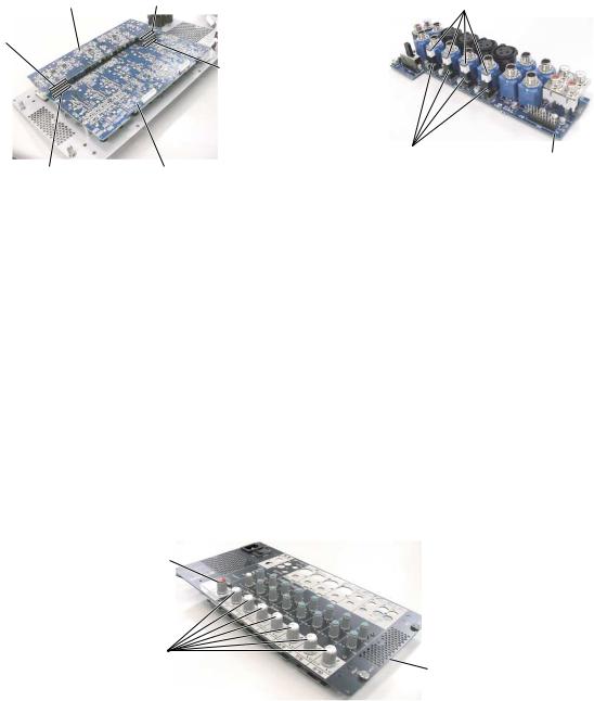
15. CONTROL2 (2/3) Circuit Board |
15. |
CONTROL2 (2/3) 9 |
||||||
(Time required: About 9 minutes) |
15-1 Ass'y 6 |
|||||||
15-1 Remove the mixer assembly. (See procedure 6) |
15-2 8 |
|||||||
15-2 Remove the rear case. (See procedure 8) |
15-3 2 9 |
|||||||
15-3 Remove the shield bracket 2. (See procedure 9) |
15-4 DSP 11 |
|||||||
15-4 Remove the DSP circuit board. (See procedure 11) |
15-5 |
1 Ass'y |
||||||
15-5 Remove the shield bracket 1 assembly. |
|
13 |
|
|
||||
(See procedure 13) |
|
|
15-6 |
CONTROL1 (1/3) 14 |
||||
15-6 Remove the CONTROL1 (1/3) circuit board. |
15-7 |
[80] VR 7 [90] |
||||||
(See procedure 14) |
|
|
|
VR 1 22 |
||||
15-7 Remove the seven (7) volume knobs (white) marked |
|
|
|
|
||||
[80] and the volume knob (red) marked [90] from |
|
|
|
|
||||
the panel printing side. (Photo 22) |
|
|
|
|
||||
[90]: Volume knob (Red) ( VR( ))
[80]: Volume knob (White) |
|
( VR( )) |
Panel assembly |
|
( Ass'y) |
Photo 22 ( 22)
13
STAGEPAS 500
15-8 |
Remove the five (5) screws marked [110]. The |
15-8 |
[110] 5 CONTROL2 (2/3) |
|||||||||
|
CONTROL2 (2/3) circuit board can then be |
|
23 |
|
|
|||||||
|
removed. (Photo 23) |
|
|
|
|
CONTROL2 (2/3) |
||||||
* |
The following parts are not parts of the |
|
CONTROL2 (2/3) |
|||||||||
|
CONTROL2 (2/3) circuit board. When replacing |
|
|
|||||||||
|
the CONTROL2 (2/3) circuit board, be sure to |
|
CONTROL2 (2/3) |
|||||||||
|
remove these parts and attach them to the new |
|
24 |
|
|
|||||||
|
CONTROL2 (2/3) circuit board. (Photo 24) |
|
[40]: |
|
|
7 |
||||||
|
• [40]: |
Push buttons |
|
7 pcs. |
|
[50B]: |
VR S |
1 |
||||
|
• [50B]: Volume knob (S) (white) |
1 pc. |
|
[60]: |
VR S |
14 |
||||||
|
• [60]: |
Volume knobs (S) (green) |
14 pcs. |
|
[70]: |
VR S |
1 |
|||||
|
• [70]: |
Volume knob (S) (blue) |
1 pc. |
|
|
|
|
|
|
|
||
|
|
[110] |
|
|
|
|
||||||
|
|
CONTROL2 (2/3) |
|
[50B]: Volume knob (S) (White) [70]: Volume knob (S) (Blue) ( VR(S)( )) |
||||||||
|
|
|
|
|
|
( VR(S)( )) |
[40]: Push button ( ) |
|||||
|
|
|
|
[110] |
|
|
|
|
|
|
|
|
|
|
|
|
|
|
[40]: Push button |
|
|
|
|
[60]: Volume knob (S) (Green) |
|
|
[110]: Bind Head Screw BIND |
( ) |
|
CONTROL2 (2/3) |
|
|||||||
|
|
|
|
( VR(S)( )) |
||||||||
|
|
|
|
|
|
|
||||||
|
|
M3.0X8 CR3 (AAX61910) |
|
|
|
|
|
Photo 24 ( 24) |
|
|||
|
|
Photo 23 ( 23) |
|
|
|
|
|
|
||||
|
|
|
|
|
|
|
|
|
|
|
||
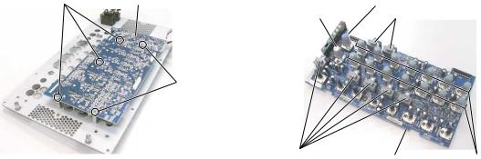
16. |
Power Switch, AC Inlet |
|
|
16. |
AC |
|||||||
|
(Time required: About 5 minutes) |
|
|
|
5 |
|
|
|||||
16-1 Remove the mixer assembly. (See procedure 6) |
16-1 Ass'y 6 |
|||||||||||
16-2 Remove the rear case. (See procedure 8) |
16-2 8 |
|||||||||||
16-3 Remove the shield bracket 2. (See procedure 9) |
16-3 2 9 |
|||||||||||
16-4 Remove the shield bracket 1 assembly. |
16-4 |
1 Ass'y |
||||||||||
|
(See procedure 13) |
|
|
|
|
13 |
|
|
||||
16-5 |
Remove the two (2) connector assemblies |
16-5 AC |
||||||||||
|
(connector assembly (1P) and connector assembly |
|
2 1P, 2P |
|||||||||
|
(2P)) and earth wire soldered to the power switch |
|
3 |
|
|
|||||||
|
and AC inlet. (Fig. 3) |
|
|
|
16-6 4 |
|||||||
16-6 Remove the power switch by pressing its claws. (Fig. 4) |
16-7 |
AC 5 |
||||||||||
16-7 Remove the AC inlet by pressing its claws. (Fig. 5) |
|
|
|
|
|
|
|
|||||
17. |
Fan (Time required: About 5 minutes) |
17. 5 |
|
|||||||||
17-1 Remove the mixer assembly. (See procedure 6) |
17-1 Ass'y 6 |
|||||||||||
17-2 Remove the rear case. (See procedure 8) |
17-2 8 |
|||||||||||
17-3 Remove the shield bracket 2. (See procedure 9) |
17-3 2 9 |
|||||||||||
17-4 Remove the shield bracket 1 assembly. |
17-4 |
1 Ass'y |
||||||||||
|
(See procedure 13) |
|
|
|
|
13 |
|
|
||||
17-5 Remove the four (4) screws marked [210]. The fan |
17-5 [210] 4 1 |
|||||||||||
|
can then be removed from the shield bracket 1 |
|
Ass'y 25 |
|||||||||
|
assembly. (Photo 25) |
|
|
|
|
|
||||||
* The fan is fixed with two-sided tape. Apply |
|
|
||||||||||
|
power little by little to remove the fan. |
|
|
|
|
|
|
|
||||
14
STAGEPAS 500
Soldering ( )
Power switch ( )
Power switch |
(brown) |
|
(blue) |
( ) |
|
( ) |
|
( ) |
|
|
|
 Panel ( )
 Connector assembly (1P) (brown)
( 1P ( ))
 Earth wire (green)
  ( ( ))
 AC inlet
  (AC )
(AC )
Soldering ( )
|
Connector assembly (2P) |
|
|
( 2P) |
Panel ( ) |
|
Fig.3 ( 3) |
|
|
|
|
|
Claw ( ) |
|
Claw ( ) |
Claw |
Claw ( ) |
( ) |
|
|
AC inlet |
Panel ( ) |
(AC ) |
Fig.4 ( 4) |
Fig.5 ( 5) |
|
[210] |
|
Fan ( ) |
Shield bracket 1 assembly ( 1 Ass'y)
[210]
[210]: Bind Head Tapping Screw-B B BIND 3.0X20 NI-BL (WK008800)
Photo 25 ( 25)
15
STAGEPAS 500
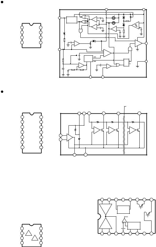
 LSI PIN DESCRIPTION LSI
YMW767-VTZ (X6055A00) CPU (SWL01B) |
|
|
|
DSP: IC1007 |
||||
PIN |
NAME |
I/O |
FUNCTION |
PIN |
NAME |
I/O |
FUNCTION |
|
NO. |
NO. |
|||||||
|
|
|
|
|
|
|||
|
|
|
|
|
|
|
|
|
1 |
Vss |
- |
Ground |
65 |
Vss |
- |
Ground |
|
2 |
TESTN |
I |
Input for TEST |
66 |
IOVDD |
- |
Power supply +3.3 V |
|
3 |
PLLBPN |
I |
PLL bypass select |
67 |
LBN/LWRN/PF6 |
O |
External memory lower-byte enable / Port F |
|
4 |
PLLVDD |
- |
PLL Power supply +2.5 V |
68 |
UBN/UWRN/PF7 |
O |
External memory upper-byte enable / Port F |
|
5 |
CIN |
- |
Capacitor terminal for PLL |
69 |
RDN/PF4 |
O |
External memory read enable / Port F |
|
6 |
PLLVss |
- |
PLL Ground |
70 |
MD00 |
I/O |
|
|
7 |
TRSTN |
I |
|
71 |
MD08 |
I/O |
|
|
8 |
TMS |
I |
JTAG input |
72 |
MD01 |
I/O |
|
|
9 |
TCK |
I |
73 |
MD09 |
I/O |
External memory data bus |
||
|
||||||||
10 |
TDI |
I |
|
74 |
MD02 |
I/O |
|
|
11 |
TDO |
O |
JTAG output |
75 |
MD10 |
I/O |
|
|
12 |
XI |
I |
Crystal oscillator |
76 |
MD03 |
I/O |
|
|
13 |
XO |
O |
Crystal oscillator |
77 |
Vss |
- |
Ground |
|
14 |
Vss |
- |
Ground |
78 |
MD11 |
I/O |
|
|
15 |
VDD |
- |
Power supply +2.5 V |
79 |
MD04 |
I/O |
|
|
16 |
ICN |
I |
Hardware reset |
80 |
MD12 |
I/O |
|
|
17 |
ECSN |
I |
CPU I/F chip select |
81 |
MD05 |
I/O |
|
|
18 |
EWRN/PD5 |
I |
CPU I/F write enable / Port D |
82 |
MD13 |
I/O |
External memory data bus |
|
19 |
ERDN/PD4 |
I |
CPU I/F read enable / Port D |
83 |
MD06 |
I/O |
|
|
20 |
EA3/PD3 |
I |
|
84 |
MD14 |
I/O |
|
|
21 |
EA2/PD2 |
I |
CPU I/F address bus / Port D |
85 |
MD07 |
I/O |
|
|
22 |
EA1/PD1 |
I |
86 |
MD15 |
I/O |
|
||
|
|
|||||||
23 |
EA0/PD0 |
I |
|
87 |
WRN/PF5 |
O |
|
|
24 |
IOVDD |
- |
Power supply +3.3 V |
88 |
Vss |
- |
Ground |
|
25 |
ED0/PC0 |
I/O |
|
89 |
VDD |
- |
Power supply +2.5 V |
|
26 |
ED1/PC1 |
I/O |
|
90 |
IOVDD |
- |
Power supply +3.3 V |
|
27 |
ED2/PC2 |
I/O |
|
91 |
MA17 |
O |
|
|
28 |
ED3/PC3 |
I/O |
CPU I/F data bus / Port C |
92 |
MA16 |
O |
|
|
29 |
ED4/PC4 |
I/O |
93 |
MA15 |
O |
|
||
|
|
|||||||
30 |
ED5/PC5 |
I/O |
|
94 |
MA14 |
O |
|
|
31 |
ED6/PC6 |
I/O |
|
95 |
MA13 |
O |
|
|
32 |
ED7/PC7 |
I/O |
|
96 |
MA12 |
O |
|
|
33 |
Vss |
- |
Ground |
97 |
MA11 |
O |
External memory address bus |
|
34 |
IRQ0N/PH0 |
I |
Interrupt input / Port H |
98 |
MA10 |
O |
|
|
35 |
TxD0 |
O |
Serial output |
99 |
MA09 |
O |
|
|
36 |
RxD0 |
I |
Serial input |
100 |
MA08 |
O |
|
|
37 |
TxD1/PG2 |
O |
Serial output / Port G |
101 |
MA07 |
O |
|
|
38 |
RxD1/PH1 |
I |
Serial input / Port H |
102 |
MA06 |
O |
|
|
39 |
SCLK1/PH2 |
I |
External synchronization clock / Port H |
103 |
MA05 |
O |
|
|
40 |
SDO |
O |
Serial output |
104 |
Vss |
- |
Ground |
|
41 |
SDI/PH3 |
I |
Serial input / Port H |
105 |
MA04 |
O |
|
|
42 |
BCLK |
O |
Bit clock output |
106 |
MA03 |
O |
External memory address bus |
|
43 |
WCLK/SYO |
O |
Word clock output |
107 |
MA02 |
O |
||
|
||||||||
44 |
SYSCLK/PG3 |
O |
Clock output / Port G |
108 |
MA01 |
O |
|
|
45 |
Vss |
- |
Ground |
109 |
CS0N/PG0 |
O |
External memory chip select / Port G |
|
46 |
VDD |
- |
Power supply +2.5 V |
110 |
MA18 |
O |
External memory address bus |
|
47 |
IOVDD |
- |
Power supply +3.3 V |
111 |
MA19 |
O |
||
|
||||||||
48 |
PA0 |
I/O |
|
112 |
MA21/PF1 |
O |
External memory address bus / Port F |
|
49 |
PA1 |
I/O |
|
113 |
MA22/PF2 |
O |
||
|
|
|||||||
50 |
PA2 |
I/O |
|
114 |
MA20 |
O |
External memory address bus |
|
51 |
PA3 |
I/O |
I/O port A |
115 |
MA23/PF3 |
O |
External memory address bus / Port F |
|
52 |
PA4 |
I/O |
116 |
CSIN/PG1 |
O |
External memory chip select / Port G |
||
|
||||||||
53 |
PA5 |
I/O |
|
117 |
MA00/PF0 |
O |
External memory address bus / Port F |
|
54 |
PA6 |
I/O |
|
118 |
Vss |
- |
Ground |
|
55 |
PA7 |
I/O |
|
119 |
VDD |
- |
Power supply +2.5 V |
|
56 |
Vss |
- |
Ground |
120 |
IOVDD |
- |
Power supply +3.3 V |
|
57 |
PB0 |
I/O |
|
121 |
CS2N/PE0 |
O |
|
|
58 |
PB1 |
I/O |
|
122 |
CS3N/PE1 |
O |
|
|
59 |
PB2 |
I/O |
|
123 |
CS4N/CASN/PE2 |
O |
|
|
60 |
PB3 |
I/O |
I/O port B |
124 |
CS5N/PE3 |
O |
External memory chip select / Port E |
|
61 |
PB4 |
I/O |
125 |
CS50RDN/PE4 |
O |
|||
|
|
|||||||
62 |
PB5 |
I/O |
|
126 |
CS51WRN/PE5 |
O |
|
|
63 |
PB6 |
I/O |
|
127 |
CS52WRN/PE6 |
O |
|
|
64 |
PB7/SYI |
I/O |
|
128 |
CS53WRN/RASN/PE7 |
O |
|
|
16

 AK5381VT (X8575A00) ADC (Analog to Digital Converter)
STAGEPAS 500
DAC1A:DSP: IC1004IC401
PIN |
NAME |
I/O |
FUNCTION |
PIN |
NAME |
I/O |
FUNCTION |
|
NO. |
NO. |
|||||||
|
|
|
|
|
|
|||
1 |
AINR |
I |
Rch Analog input pin |
9 |
SDTO |
O |
Audio serial data output pin |
|
2 |
AINL |
I |
Lch Analog input pin |
10 |
LRCK |
I/O |
Output channel clock pin |
|
3 |
CKS1 |
I |
Mode select 1 pin |
11 |
MCLK |
I |
Master clock input pin |
|
4 |
VCOM |
O |
Common voltage output pin |
12 |
SCLK |
I/O |
Audio serial data clock pin |
|
5 |
AGND |
- |
Analog ground |
13 |
PDN |
I |
Power down mode pin |
|
6 |
VA |
- |
Analog power supply +5V |
14 |
DIF |
I |
Audio interface format pin |
|
7 |
VD |
- |
Digital power supply +3.3V |
15 |
CKS2 |
I |
Mode select 2 pin |
|
8 |
DGND |
- |
Digital ground |
16 |
CKS0 |
I |
Mode select 0 pin |
PCM1742EK (X8574A00) DAC (Digital to Analog Converter) |
DAC1A:DSP: IC1008IC401 |
|||||||
PIN |
NAME |
I/O |
FUNCTION |
PIN |
NAME |
I/O |
FUNCTION |
|
NO. |
NO. |
|
||||||
|
|
|
|
|
|
|
||
1 |
BCK |
I |
Audio data bit clock input |
9 |
AGND |
- |
Analog ground |
|
2 |
DATA |
I |
Audio data digital input |
10 |
VcoM |
- |
Common voltage decoupling |
|
3 |
LRCK |
I |
L-channel and R-channel audio-data latch-enable input |
11 |
ZEROR/ZEROA |
O |
Zero-flag output for R-channel/Zero-flag output for L-/R-channel |
|
4 |
DGND |
- |
Digital ground |
12 |
ZEROL/NA |
O |
Zero-flag output for L-channel/No assign |
|
5 |
VDD |
- |
Digital power supply +3.3V |
13 |
MD |
I |
Mode control data input |
|
6 |
Vcc |
- |
Analog power supply +5V |
14 |
MC |
I |
Mode control clock input |
|
7 |
VOUTL |
O |
Analog output for L-channel |
15 |
ML |
I |
Mode control latch input |
|
8 |
VOUTR |
O |
Analog output for R-channel |
16 |
SCK |
I |
System clock input |
|
17
STAGEPAS 500
 IC BLOCK DIAGRAM IC
FA3641N (X8570A00) |
|
|
PWM Control |
CS |
VCC |
POWER: IC803 |
8 |
6 |
|
|
|
|
|
|
|
|
|
|
|
0.82V~0.68V |
|
6.5 A |
15.5V |
|
|
|
|
|
REF |
7 |
5V |
VCC |
|
|
+ |
|
|
|
|
|
|
|
|
|
|
|
ENB |
|
|
– |
|
|
|
UVLO |
|
|
|
|
|
|
|
|
|
|
|
|
|
|
||
|
|
|
|
|
|
|
|
|
|
|
15.5V |
+ |
|
|
|
|
|
|
|
5V REF |
|
|
|
|
|
|
|||
|
|
|
|
|
|
|
+ |
|
0.9mA |
|
|
|
||
|
|
|
|
|
|
|
|
|
|
|
– |
|
||
RTRch |
1 |
8 |
CS |
|
|
|
|
|
– |
|
+ |
|
|
|
|
|
|
|
|
|
|
|
8.5V~7.9V |
|
– |
|
16.5V/9V |
|
|
FB |
2 |
7 |
REF |
|
|
|
|
|
0.8V |
|
|
|
||
|
|
|
|
|
|
|
|
|
|
|||||
IS(+)/IS(-) |
3 |
6 |
VCC |
|
|
|
|
|
|
|
|
|
ENB |
|
|
|
|
|
|
3.0V |
|
|
|
|
|
|
|
||
GND |
4 |
5 |
OUT |
|
|
+ |
|
|
4V |
|
|
|
5 |
OUT |
|
|
|
|
|
|
– |
|
|
|
|
|
|||
|
|
|
|
|
|
|
|
|
|
|
|
|
|
|
|
|
|
|
|
|
|
|
|
|
|
|
|
OUTPUT |
|
|
|
|
FB |
2 |
|
|
|
|
|
– |
|
|
|
|
|
|
|
|
|
|
|
|
|
|
– |
|
|
|
|
|
|
|
|
|
|
Dmax |
|
|
|
–PWM |
|
|
|
|
|
|
|
|
|
|
|
|
|
|
+ |
|
|
|
|
|
|
|
|
|
|
70% |
|
OSC |
|
|
|
FF |
|
|
|
|
|
|
|
|
|
RM RT |
0.24V |
|
|
R QB |
4 |
GND |
|
|
|
|
|
|
|
+ |
|
|
|
|
Q |
|
|
|
|
|
|
|
|
|
|
|
|
|
– |
|
|
||
|
|
|
|
|
|
– |
|
|
|
|
S |
|
|
|
|
|
|
|
|
|
|
|
|
|
+ |
|
|
|
|
|
|
|
|
|
|
|
|
|
|
|
|
|
|
|
|
|
|
|
|
|
|
|
1 |
|
3 |
|
|
|
|
|
|
|
|
|
|
|
|
RT |
IS + |
|
|
|
|
|
LB1407-E LF (AAX68710) |
|
|
|
|
|
|
|
|
|
|
|
|||
AC/DC Voltage Level Meter |
|
|
|
|
|
|
|
|
|
|
|
|||
CONTROL2 (2/3): IC604 |
|
|
|
|
|
|
|
|
|
|
|
|
||
|
|
|
|
|
|
|
|
|
|
|
|
12, 11, 10, 9 |
|
|
|
|
|
|
|
|
Vref Vcc |
Rch |
|
D7 |
D6 |
|
D1 |
|
|
|
|
|
|
|
|
3 |
1 |
2 |
|
14 |
13 |
|
8 |
|
Vcc |
1 |
14 |
D7 |
|
|
|
|
|
|
|
|
|
|
|
Rch |
2 |
13 |
|
|
|
|
|
|
R7 |
|
R6 |
|
R1 |
|
D6 |
|
|
|
|
|
5.83 kΩ |
|
4.12 kΩ |
|
1 kΩ |
|
|||
|
|
|
|
|
|
|
|
|
|
|
|
|||
Vref |
3 |
12 |
D5 |
|
|
|
|
|
-- |
|
-- |
-- |
|
|
IN+ |
|
|
|
|
|
|
|
|
COM |
|
COM |
|
COM |
|
4 |
11 |
D4 |
|
|
|
|
|
7 |
|
6 |
|
1 |
|
|
|
|
|
|
|
+ |
|
+ |
+ |
|
|
||||
IN-- |
5 |
10 |
IN + |
|
4 |
|
|
|
|
|
|
|
|
|
D3 |
|
|
|
|
|
|
|
|
|
|
|
|||
|
|
|
IN -- |
|
5 |
|
|
|
|
|
|
|
|
|
OUT |
6 |
9 |
D2 |
|
|
|
|
|
|
|
|
|
|
|
GND |
7 |
8 |
D1 |
|
|
|
|
|
|
|
|
|
|
|
|
|
|
|
|
|
6 |
7 |
|
|
|
|
|
|
|
|
|
|
|
|
|
OUT |
GND |
|
|
|
|
|
|
|
 NJM2068M-D TE1 (AAX62750)
Dual Operational Amplifier
CONTROL1 (1/3): IC101, 201, 501, 701, 704 CONTROL2 (2/3): IC102, 104-106, 108, 202,
|
|
|
|
|
203, 205, 206, 302, 402, |
|||||||||
|
|
|
|
|
502, 503, 702, 703, 901, |
|||||||||
|
|
|
|
|
902 |
|
||||||||
CONTROL3 (3/3): IC541, 542 |
||||||||||||||
DSP: |
|
|
|
|
|
|
IC103, 107, 204, 603, 1009, |
|||||||
|
|
|
|
|
1011 |
|
||||||||
Output A |
1 |
|
|
|
|
|
|
|
|
|
+V 8 |
+DC Voltage |
||
Inverting |
|
|
|
|
|
|
|
|
|
|
|
|
|
Supply |
2 |
|
|
|
|
|
|
|
|
|
|
|
7 |
Output B |
|
Input A |
|
|
- |
|
+ |
|
|
|
|
|
|
Inverting |
||
Non-Inverting |
3 |
|
|
|
|
|
|
|
|
|
|
6 |
||
|
|
|
|
|
|
|
|
|
|
|||||
Input A |
|
|
|
|
+ - |
|
|
|
Input B |
|||||
-DC Voltage Supply |
4 |
-V |
|
|
|
|
|
|
|
|
5 |
Non-Inverting |
||
|
|
|
|
|
|
|
|
|||||||
|
|
|
|
|
|
|
|
|||||||
Input B
 PC494GS-T2-A (X8569A00)
Switching Regulator
POWER: IC802
Non-Inv. |
Inv. |
Ref |
Output |
Vcc |
C2 |
E2 |
E1 |
Input |
Input |
Out |
Control |
||||
16 |
15 |
14 |
13 |
12 |
11 |
10 |
9 |
+ |
– |
|
|
|
|
|
|
ERROR |
REFERENCE |
|
|
|
|
||
AMP |
|
|
|
|
|||
2 |
|
REGULATOR |
|
|
|
|
|
ERROR |
|
|
|
|
|
|
|
AMP |
|
OSCILLATOR |
|
|
|||
+ 1 |
– |
0.1V |
|
|
|
|
|
1 |
2 |
3 |
4 |
5 |
6 |
7 |
8 |
Non-Inv. |
Inv. |
Feed- |
Dead- |
CT |
RT |
GND |
C1 |
Input |
Input |
Back |
Time |
|
|
|
|
Control
18
STAGEPAS 500
 CIRCUIT BOARDS
AMP Circuit Board (4200-30) ................................................................... |
26 |
CONTROL1 (1/3) Circuit Board (6486-30) ............................................... |
24 |
CONTROL2 (2/3) Circuit Board (6486-30) ......................................... |
22/23 |
CONTROL3 (3/3) Circuit Board (6486-30) ............................................... |
25 |
DSP Circuit Board (1043-40) .................................................................... |
19 |
JACK Circuit Board (5254B-30) ............................................................... |
25 |
NETWORK Circuit Board (5254A-30) ...................................................... |
26 |
POWER Circuit Board (8146-40) ........................................................ |
20/21 |
Note: See parts list for details of circuit board component parts.
:
 DSP Circuit Board
not installed
* 1
* 1 |
+ |
C1012 |
– |
|
|
|
|
|
|
|
|
|
|
|
|
|
|
|
|
|
|
|
|
|
|
|
|
|
|
|
|
|
|
|
|
|
|
|
|
|
|
|
|
|
|
|
|
|
|
|
|
|
|
|
|
|
|
|
|
|
|
|
|
|
|
|
|
|
|
|
|
|
|
|
|
|
|
|
|
|
|
|
|
|
|
|
|
|
|
|
|
|
|
|
|
|
|
|
|
|
|
|
|
|
|
|
|
|
|
|
|
|
|
|
|
|
|
|
|
|
|
|
|
|
|
|
|
|
|
|
|
|
|
|
|
|
|
|
|
|
|
|
|
|
|
|
|
|
|
|
|
|
|
|
|
|
|
|
|
|
|
|
|
|
|
|
|
|
|
|
|
|
|
|
|
|
|
|
|
|
|
|
|
|
|
|
|
|
|
|
|
|
|
|
|
|
|
|
|
|
|
|
|
|
|
|
|
|
|
|
|
|
|
|
|
|
|
|
|
|
|
|
|
|
|
|
|
|
|
|
|
|
|
|
|
|
|
|
|
|
|
|
|
|
|
|
|
|
|
|
|
|
|
|
|
|
|
|
|
|
|
|
|
|
|
|
|
|
|
|
|
|
|
|
|
|
|
|
|
|
|
|
|
|
|
|
|
|
to CONTROL2 (2/3)-CN33 |
|
|
|
|
|
|
|
|
|
|
|
|
|
to CONTROL2 (2/3)-CN27 |
||||||||||||||||||||||||||||||||||||||||||
Component side
* 2 |
* 2 |
C1013 |
Pattern side
444608
19

STAGEPAS 500
 POWER Circuit Board
to POWER switch |
|
to FAN |
||||||||||||
AC IN |
to CONTROL3 |
(3/3)-CN541 |
|
|
to CONTROL2 (2/3)-CN1 |
|||||||||
|
|
|
|
|
||||||||||
|
|
|
|
|
|
|
|
|
|
|
|
|
|
|
|
|
|
|
|
|
|
|
|
|
|
|
|
|
|
|
|
|
|
|
|
|
|
|
|
|
|
|
|
|
|
|
|
|
|
|
|
|
|
|
|
|
|
|
|
|
|
|
|
|
|
|
|
|
|
|
|
|
|
|
Component side
444598 (J, U, C), 444744 (B, H, O)
20
STAGEPAS 500
 POWER Circuit Board
Pattern side
444598 (J, U, C), 444744 (B, H, O)
21
Loading...