


FOREWORD
This publication is intended to aid the electronic technician in servicing the CTC175/176/177 television chassis. It will explain the theory of operation, highlighting new and different circuits associated with the digitally controlled chassis. This manual focuses on: PIP, Tuner- On-Board and System Control circuitry. It is designed to help the technician become more familiar with the chassis layout, increase confidence and improve overall efficiency in servicing the product.
Note: This publication is intended to be used only as a training aid. It is not intended to replace service data. Thomson Consumer Electronics Service Data for these instruments contains specific information about parts, safety and alignment procedures and must be consulted before performing any service. The information in this publication is as accurate as possible at the time of publication. Circuit designs and drawings are subject to change without notice.
SAFETY INFORMATION CAUTION
Safety information is contained in the appropriate Thomson Consumer Electronics Service Data. All product safety requirements must be compiled with prior to returning the instrument to the consumer. Servicers who defeat safety features or fail to perform safety checks may be liable for any resulting damages and may expose themselves and others to possible injury.
All integrated circuits, all surface mounted devices, and many other semiconductors are electrostatically sensitive and therefore require special handling techniques.
Prepared by |
|
Thomson Consumer Electronics, Inc. |
First Edition 9301 - First Printing |
Technical Training Department |
Copyright 1993 Thomson Consumer Electronics, Inc. |
600 North Sherman Drive Indianapolis, Indiana 46201 |
Trademark(s)® Registered Marca(s) Registrada(s) |
|
Printed in U.S.A. |
|
Table of Contents |
Overview ............................................................................................................... |
5 |
Power Supply ....................................................................................................... |
6 |
Troubleshooting................................................................................................. |
7 |
CTC175 Power Supply .......................................................................................... |
9 |
Troubleshooting............................................................................................... |
10 |
Standby Supplies ................................................................................................. |
10 |
Troubleshooting............................................................................................... |
10 |
System Control .................................................................................................. |
11 |
Reset Circuit ........................................................................................................ |
12 |
Data Communications ......................................................................................... |
14 |
Power-On Sequence ........................................................................................... |
18 |
U3201 - EEPROM ............................................................................................... |
19 |
Keyboard Interface .............................................................................................. |
19 |
IR Input ................................................................................................................ |
19 |
On Screen Display ............................................................................................... |
19 |
Closed Caption .................................................................................................... |
20 |
Service Menu ....................................................................................................... |
21 |
Alignment Parameters ......................................................................................... |
23 |
System Control .................................................................................................... |
25 |
Troubleshooting............................................................................................... |
25 |
Horizontal Deflection ......................................................................................... |
28 |
Horizontal AFC and APC ..................................................................................... |
30 |
Shutdown Recovery ............................................................................................. |
31 |
Troubleshooting............................................................................................... |
32 |
Pincushion Alignments......................................................................................... |
34 |
Troubleshooting............................................................................................... |
34 |
Horizontal Standby Regulator.............................................................................. |
35 |
Troubleshooting............................................................................................... |
35 |
Vertical ................................................................................................................ |
36 |
Troubleshooting............................................................................................... |
38 |
Tuning ................................................................................................................. |
39 |
CTC175/76/77 Tuner ........................................................................................... |
40 |
CTC175 Tuner Isolation Box ............................................................................... |
42 |
Tuner Alignment Generator ................................................................................. |
44 |
Troubleshooting............................................................................................... |
46 |
Tuner Voltage Charts ........................................................................................... |
48 |
Video / Audio IF .................................................................................................. |
55 |
IF Alignments ....................................................................................................... |
56 |
Luminance Processing ..................................................................................... |
59 |
Troubleshooting............................................................................................... |
60 |
Chrominance Processing ................................................................................ |
61 |
Troubleshooting............................................................................................... |
62 |
Audio Processing .............................................................................................. |
63 |
Troubleshooting............................................................................................... |
64 |
PIP ....................................................................................................................... |
65 |
User Controls ....................................................................................................... |
67 |
Alignments ........................................................................................................... |
67 |
Troubleshooting............................................................................................... |
67 |
Appendix........................................................................................................... |
72 |
Index.................................................................................................................. |
76 |
Self-Test............................................................................................................ |
77 |

Figure 1, F25190

Overview 5
PIP
Tuner
Figure 2, CTC177 Chassis
The CTC175/176/177 chassis is a new concept in television design. All three chassis OVERVIEW are very similar, with the primary differences being features and power supply. The
CTC175 chassis is a hot chassis with a linear regulator. Consequently, this version does not have audio or video jacks on the back. The CTC176 and CTC177 have a switching regulator that allows for a cold chassis.
Four innovations are incorporated in these chassis. First, all the alignments are performed digitally using the remote control. There are no potentiometers on the chassis. All alignments are stored in the EEPROM. Second, the tuner is located on the main chassis circuit board. This requires the tuner to be serviced down to the component level where it used to be a replaceable assembly. Third, the fully featured models contain a new PIP (picture in picture) circuit. It too is located on the main board and is much more integrated than similar circuits in the CTC169 chassis. There are only two IC’s: the PIP processor, U2901 and the SRAM memory, U2902. The increased integration makes troubleshooting much easier. Fourth, later versions of this chassis will contain built-in closed caption decoders for the hearing impaired. This circuitry is primarily contained within the system control microprocessor, U3101, and will require practically no service from the technician.
Different models support 20", 25", 27" and 31" screen sizes. Various option packages will accompany the different sets. Fully featured sets will have the new PIP circuit with S-Video In jacks with the standard Video/Audio In/Out jacks. The composite video jacks are used for the PIP source, as the S-Video is not routed through the PIP circuit. Stereo audio with HI-FI out jacks are also included as options.
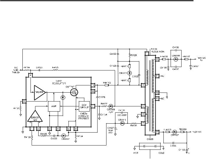
6 Power Supply
The CTC176/177 power supply is a variable frequency/variable pulse width Power Supply hybrid IC power supply. U4101, the hybrid IC, contains most of the components
including the power switching FET (Field Effect Transistor). The switching device turns on and off inducing a voltage into the secondary of the transformer. The lower the frequency, the more energy is transferred to the secondary.
Figure 3, CTC176/177 Power Supply
When power is first applied to the set, approximately 150 VDC raw B+ is developed by the bridge rectifier (CR4001 - CR4004) and filter capacitor (C4007). This is applied through the primary winding of T4101 pins 1 and 3 to U4101 pins 11 and 12. Pins 11 and 12 are connected to the drain of the power FET inside U4101. The source of the power FET is connected to pins 8 and 9. These pins are connected to ground through R4124. The start-up resistor (R4104) provides enough bias to gate the FET on through pin 4 of the IC. When the FET is turned on, the drain current flows through the primary winding of T4101, through the FET to ground. Current flowing in the primary induces a voltage between pins 5 and 6 of the transformer. This voltage is coupled from pin 5 through R4125 and C4123 to pin 4 of the regulator IC. The polarity of the voltage at pin 4 is such that it turns the FET on harder. As more current flows through the FET, the greater the voltage drop across R4124, the FET source resistor. The voltage will eventually become

Power Supply 7
large enough to turn on the over-current protection circuit (OCP) inside U4101. This will cause the FET to turn off. When the FET turns off, energy transfers to the secondary windings of T4101 charging C4107 and C4108. This repeats for several cycles and stable oscillation starts. The frequency of oscillation will vary with load from approximately 100Khz in standby to 38Khz with a full load (120 watts AC input power).
The feedback winding between pins 5 and 7 on T4101 is tightly coupled to the secondary windings. The voltage on the feedback winding will follow the voltage changes on the secondary windings. The voltage developed on pin 7 of T4101 is rectified by CR4111 and filtered by C4127. This negative voltage is applied to pin 1 of U4101. There is a precision voltage reference inside U4101 trimmed to -40.5 volts +/- .5 volts. The error amplifier tries to make the voltage on pin 1 of U4101 equal to the reference voltage. If the load on the secondaries increases and the voltage drops, the voltage developed at pin 7 of T4101 would decrease (less negative). This would allow the FET to stay on longer increasing the output voltage. In this way, the IC is able to hold the output of the supply constant with varying line voltages and loads.
If an excessive load is placed on the power supply outputs, the on time of the FET will increase. This will result in more current through the FET and the source resistor R4124. The voltage drop will be proportional to the current. This voltage will charge C4124 and at some point turn on the OCP circuitry in U4101 causing the FET to turn off. The value of C4124 is critical the OCP trip point.
The network composed of C4122, C4128, R4126 and CR4112 is a snubber network used to reduce the high voltage spike developed when the FET turns off. C4103 and R4105 are part of a compensation network that stabilize the supply from parasitic oscillations. R4129 is an ESD (Electrostatic Discharge) protection resistor for the gate of the FET inside U4101. R4122 and CR4109 help stabilize the OCP circuit against line voltage variations. Ferrite beads in the circuit are for RFI (Radio Frequency Interference) emission reduction. C4107, L4102 and C4105 form a filter network to reduce the ripple in the regulated B+ and reduce high frequency switching noise.
Troubleshooting
1.Measure the voltage on pin 1 of U4101. It should be -40.5 volts +/- 0.50 volts. If it is correct, the IC is probably working. If it is not correct, there is most likely an abnormal load on the power supply. As the output loads increase above the design ratings, the output voltages and the oscillation frequency will drop. If the loads are high enough, the frequency of the power supply will be in the audible range. If there is a short on the secondary of T4101, the supply will shut down until the short is removed. Under normal conditions, a short on the secondary will not damage the supply. Under no load conditions, the regulated B+ will rise and the supply will go into a burst mode where there is a series of burst pulses.
D I G I T A

8 Power Supply
Figure 4, CTC176/177 Power Supply
Note: It is not recommended running the supply with no load. The output filter capacitors may be stressed by over-voltage.
2.If pin 1 of U4101 is shorted, the regulated 140 volt B+ will be low, approximately 30 volts. If pin 1 is open, the regulated 140 volt B+ will rise to over 200 volts.
3.If F4001 blows, U4101 is most likely shorted.
4.If regulated B+ is too low, suspect an excessive output load, defective T4101 or a shorted C4127.
5.If regulated B+ is too high, suspect a no-load condition on the secondary of T4101 or an open in the feedback path to pin 1 on U4101.
Note: It is normal for the 140 volt supply to rise 4 or 5 volts in the standby mode.
6.If the supply will not oscillate, suspect a defective U4101, T4101, R4104, R4125 or C4123.
7.For poor regulation, suspect a defective T4101, U4101, C4103 or R4105.

Power Supply 9
Power Supply
The power supply in the CTC175 is a simple series pass regulator with microprocessor controllability. 150 volts raw B+ is applied to the collector of Q4150, an integrated darlington regulator. R4155 passes a portion of the total current around Q4150 to minimize current dissipation in the transistor. The output of the regulator is filtered by C4153.
The feedback loop for the supply begins with a voltage divider made up of R4157 and R4158. The divider feeds the input of a comparator at pin 30 of U1001. A PWM (pulse width modulated) output from pin 28 of U1001 feeds Q4153 inverting the control voltage to the base of Q4151. Q4151 controls the base bias of Q4150. As a load increases on the 140B+ supply, the voltage to pin 30 drops, causing the PWM output from pin 28 of U1001 to increase, forward biasing Q4153 harder. This in turn reduces the base bias to Q4151 increasing the forward bias on Q4150, increasing the B+ output of the power supply.
The PWM circuit inside U1001 is also affected by beam current via the size compensation input pin 16 which is also used in the vertical circuit to minimize raster blooming (see vertical circuit). This helps stabilize the linear regulator during heavy beam current transitions. As beam current increases, regulator output decreases.
TANDBY |
1 |
U4102 |
3 |
|
|
|
+12V STBY |
|
|
|
|
||||
B+ |
|
|
|
|
|
|
C4104 |
|
|
|
|
R4103 |
|
|
|
|
|
|
|
|
|
|
|
|
|
2 |
|
+5V STBY |
|
|
|
|
|
|
|
|
|
|
|
|
|
|
|
REGULATORS |
|
|
|
|
|
CR4103 |
|
Q4103 |
|
|
|
|
|
|
|
|
|
|
|
|
|
|
|
|
|
|
+5V STBY2 |
|
|
|
|
R4108 |
C4111 |
+ |
C4118 |
|
|
|
R4111 |
|
|
|
|
|
|
|
CR4104 |
Q4105 |
|
|
|
|
|
|
|
|
|
|
|
|
|
|
5.6V |
C4114 |
|
|
+5V STBY1 |
|
|
|
|
R4112 |
+ |
|
|
|
|
|
|
C4112 |
|
|
|
|
|
|
|
|
|
|
+5V REF |
Figure 5, CTC175 Power Supply
10 Power Supply
Failures of the linear regulator can be difficult to detect if the AC line voltage is
Troubleshooting constant. Using a variac to check proper regulation is the best approach. If the regulator circuit is suspected of being defective, perform the following steps:
|
|
1. Apply 105 to 130 VAC to the TV and check the 140 B+ output. If the B+ is |
|
|
|
|
|
not 140 volts, enter the service alignments and attempt to raise and lower the |
|
|
|
D I G I T |
A |
|
|
|
B+ with the digital “B+ Trim” adjustment (parameter #18). If the adjustment |
|
|
has no effect, go to the next step. If the 140 B+ can be set, the circuit is most |
|
|
likely functioning correctly. |
2.Monitor the collector voltages on Q4153 and Q4151. The voltages should increase and decrease inversely as the B+ trim adjustment is performed. If this is not the case, suspect Q4153 or Q4151. If the voltage varies with the alignment, but the B+ does not change, suspect a defective Q4150.
T E C
T I P
Standby
Supplies
HNote: A shorted horizontal output, Q4401, will most likely cause Q4150 to short. Always check Q4150 after replacing a defective Q4401.
The standby supplies provide a Standby 12 volt supply, two Standby 5 volt supplies and one 5.6 volt reference supply. Approximately 20 volts, from the switching supply on the CTC176/177 or the standby bridge rectifier on the CTC175, is applied to pin 1 of U4102, a three-legged 12 volt regulator. The output on pin 3 serves as the 12 volt standby supply. The 12 volt supply is also applied to the cathode of CR4104, a 5.6 volt zener diode, that sets up the base bias for Q4103 and Q4105. A portion of the 12 volts is sent to the collectors of the same transistors for the voltage source. The voltage drop across of the base emitter junction of the transistors produces the 5 volt supplies on their emitters.
STANDBY |
1 |
U4102 |
3 |
|
|
|
+12V STBY |
|
|
|
|
|
|||
B+ |
|
|
|
|
|
|
C4104 |
|
|
|
|
R4103 |
|
|
|
|
|
|
|
|
|
|
|
|
|
2 |
|
+5V STBY |
|
|
|
|
|
|
|
|
|
|
|
|
|
|
|
REGULATORS |
|
|
|
|
|
CR4103 |
|
Q4103 |
|
|
|
|
|
|
|
|
|
|
|
|
|
|
|
|
|
|
+5V STBY2 |
|
|
|
|
R4108 |
C4111 |
+ |
C4118 |
|
|
|
R4111 |
|
|
|
|
|
|
|
CR4104 |
Q4105 |
|
|
|
|
|
|
|
|
|
|
|
|
|
|
5.6V |
C4114 |
|
|
+5V STBY1 |
|
|
|
|
R4112 |
+ |
|
|
|
|
|
|
C4112 |
|
|
|
|
|
|
Figure 6, Standby Supplies |
|
|
+5V REF |
|
Troubleshooting |
|
|
|
||||
|
|
|
|
|
|||
D I G I T A
1. Check the 12 volt supply on pin three of U4102.
2.Check the 5.6 volt reference on the cathode of CR4104.
3.Check the 5 volt standby 1 and 2 supplies on the emitter of Q4105 and Q4103 respectively.

|
System Control 11 |
|
The CTC177 chassis family is a digitally controlled television receiver. The system |
System |
|
control circuit governs the entire television. The control circuits are not only |
Control |
|
responsible for turning the set on and off, but also for aligning the different circuits |
||
|
||
such as deflection and signal. Adjustments once made by adjusting a potentiometer |
|
|
or coil are now performed by reading and writing data to the EEPROM (Electrically |
|
|
Erasable Programmable Read Only Memory) using an on-screen menu and the |
|
|
television’s remote control. |
|
A newly developed television processing IC, called the T-Chip (Thomson Chip), exchanges information with the system control microprocessor over the serial data bus. This communication is carried out over a three wire bus utilizing the new T-Bus (Thomson Bus) protocol. The T-Chip implements a new level of integration by housing more circuitry than ever before, and reducing the number of external peripheral components.
The system control microprocessor can decode Line 21 closed caption information and display the text on the screen. When implemented, the customer will be able to selectively view the text on closed captioned encoded programs.
1,2,3 |
GND U3201 |
U2901 GND |
3,5 |
15,16 |
|||
4,7 |
EEPROM |
D-PIP |
40,41 |
|
|||
|
|
|
|
|
|
|
|
|
|
|
|
|
|
|
|
|
|
|
|
|
|
|
|
|
|
5V |
|
|
8 |
|
|
|
|
|
|
|
|
|
|
|
|
|
|
|
|
|
|
|
|
|
|
|
|
|
|
|
|
|
|
|
|
|
VDD |
|
39 |
|
|
|
|
|
|
5V |
|
|||||||||||||||||||||||||||
|
|
|
|
|
|
|
|
|
|
|
|
|
|
|
|
|
|
|
|
|
|
|
|
|
|
|
VDD |
|
|
|
|
|
|
|
|
|
|
|
|
|
|
|
|
|
|
|
|
|
|
|
|
|
|
|
|
|
|
|
|
|
||||||||||||||||||||||||||||||||||||||
|
|
|
|
|
|
|
|
|
|
|
|
|
|
|
|
|
|
|
|
|
|
|
|
|
|
|
|
|
|
|
|
|
|
|
|
|
|
|
DATA |
|
|
CLOCK |
|
|
|
DATA CLOCK ENABLE |
|
|
|
|
|
|
|
|
|
|
|
|
|
|
|
|
|
|
|
|
|
|
|
|
||||||||||||||||||||||||||||
|
|
|
|
|
|
|
|
|
|
|
|
|
|
|
|
|
|
|
|
|
|
|
|
|
|
|
|
|
|
|
|
|
|
|
|
|
|
|
|
|
|
|
|
|
|
|
|
|
|
|
|
|
|
|
|
|
|
|
|
|
|
|
|
|
|
|
|
|
|
|
|
|
|
|
|
|
|
|
|
|
|
|
|
|
|
|
|
|
|
|
|
|
|
|
|
|
||
|
|
|
|
|
|
|
|
|
|
|
|
|
|
|
|
|
|
|
|
|
|
|
|
|
|
|
|
|
|
|
|
|
|
|
|
|
|
|
|
|
5 |
|
|
|
|
|
|
6 |
|
|
|
|
20 |
|
|
|
21 |
|
22 |
|
|
|
|
|
|
|
|
|
|
|
|
|
|
|
|
|
|
|
|
|
|
|
|
|
|
|
||||||||||||
|
|
|
|
|
|
|
|
|
|
|
|
|
|
|
|
|
|
|
|
|
|
|
|
|
|
|
|
|
|
|
|
|
|
|
|
|
|
|
|
|
|
|
|
|
|
|
|
|
|
|
|
|
|
|
|
|
|
|
|
|
|
|
|
|
|
|
|
|
|
|
|
|
|
|
|
|
|
|
|
|
|
|
|
|
|
|
|
|
|
|
|
|
|
|
|
|
|
|
|
|
|
|
|
|
|
|
|
|
|
|
KS1 |
|
|
|
T-CHIP DATA |
|
15 |
|
|
|
|
|
|
|
|
|
|
|
|
|
|
|
|
|
|
|
|
|
|
|
|
|
|
|
|
|
|
|
|
|
|
|
|
|
|
|
|
|
|
|
|
|
|
|
|
|
|
|
|
|
|
|
|
|
|
|
|
|
|
|
|
||||||||||||||||
POWER |
|
|
|
6 |
|
|
|
|
|
|
|
|
TUNER CLOCK |
|
|
|
|
|
|
|
|
|
|
|
|
|
|
|
|
|
|
|
|
|
|
|
|
|
|
|
|
|
|
|
54 |
|
DATA |
|
|
|
|
|
|
|
|
|
|
|
|
|
|
|||||||||||||||||||||||||||||||||||||
|
|
|
KS2 |
|
|
T-CHIP CLOCK |
|
16 |
|
|
|
|
|
|
|
|
|
|
|
|
|
|
|
|
|
|
|
|
|
|
|
|
|
|
|
|
|
|
|
|
|
|
|
|
|
|
53 |
|
CLOCK |
|
|
|
|
|
|
|
|
|
|
|
|
|
|
|||||||||||||||||||||||||||||||||||
|
|
|
|
|
|
|
|
|
|
7 |
|
|
|
|
|
|
|
|
|
|
|
|
|
|
|
|
|
|
|
|
|
|
|
|
|
|
|
|
|
|
|
|
|
|
|
|
|
|
|
|
|
|
|
|
|
|
|
|
|
|
|
|
|
|
|
|
||||||||||||||||||||||||||||||||
VOL. UP |
|
|
|
|
|
|
|
|
|
|
|
|
|
TUNER DATA |
|
|
|
|
|
|
|
|
|
|
|
|
|
|
|
|
|
|
|
|
|
|
|
|
|
|
|
|
|
|
|
|
|
|
|
|
|
|
|
|
|
|
|
|
|
|
|
|
|
|
|
|
|
|
|
|
|
|
|
|
|
|
|
|
|
|
|
|||||||||||||||||
|
|
|
|
|
|
|
|
|
|
|
8 |
KS3 |
|
|
|
|
|
|
|
|
|
|
PIP |
|
12 |
|
|
|
|
|
|
|
|
|
|
|
|
|
|
|
|
|
|
|
|
|
|
|
|
|
|
|
|
|
|
|
|
|
|
|
|
|
|
|
|
|
|
|
|
|
|
|
|
|
|
|
|
|
|
|
|
|
|
|
|
|
|
|
|
|||||||||
VOL. DN. |
|
|
|
|
|
|
|
KD1 |
|
|
|
|
|
|
|
|
ENABLE |
|
|
|
|
|
|
|
|
|
|
|
|
|
|
|
|
|
|
|
|
|
|
|
|
|
|
|
|
|
|
|
|
|
|
|
|
|
|
|
|
|
|
|
|
|
|
|
|
|
|
|
U1001 |
|
||||||||||||||||||||||||||||
|
|
|
|
|
|
|
5 |
U3101 |
T-CHIP |
|
14 |
|
|
|
|
|
|
|
|
|
|
|
|
|
|
|
|
|
|
|
|
|
|
|
|
|
|
|
|
|
|
|
|
|
|
|
|
|
|
52 |
|
|
|
|
|
|
|
T-CHIP |
|
|||||||||||||||||||||||||||||||||||||||
CH. UP |
|
|
|
|
|
|
|
|
|
|
|
|
|
|
|
|
|
|
|
P |
ENABLE |
|
|
|
|
|
|
|
|
|
|
|
|
|
|
|
|
|
|
|
|
|
|
|
|
|
|
|
|
|
|
|
|
|
|
|
|
|
|
|
|
ENABLE |
|
|
|
|
|
|
|
|
HORZ. |
24 |
||||||||||||||||||||||||||
|
|
|
|
|
|
|
|
|
|
|
|
|
|
|
|
|
|
|
|
|
|
|
|
|
|
|
|
|
|
|
|
|
|
|
|
|
|
|
|
|
|
|
|
|
|
|
|
|
|
|
|
|
|
|
|
|
|
|
|
|
|
|
|
|
|
|
|
|
|
|
|
|
|
|
|
|
|
|
|
|
|
|
|
|
OUT |
|||||||||||||
|
|
|
|
|
|
|
|
|
|
|
|
|
|
|
|
|
|
|
|
|
|
|
|
|
|
|
|
|
|
|
|
|
|
|
|
|
|
|
|
|
|
|
|
|
|
|
|
|
|
|
|
|
|
|
|
|
|
|
|
|
|
|
|
|
|
|
|
|
|
|
|
|
|
|
|
|
|
|
|
|
|
|
|
|
|
|
|
|
|
|
|
|
|
|
|
|
|
|
CH. DN. |
|
|
|
|
1 |
5V |
|
|
|
|
|
|
|
|
RESET |
|
|
|
|
|
|||
MENU |
|
|
|
VDD |
20 |
5V |
|
|
7.6 V |
22 |
|
|
|
|
|
4 |
5 |
STBY |
|
||||
|
|
|
|
|
|
|
|||||
|
|
|
|
|
|
|
|
|
|||
5V |
3 |
OSC |
OSC |
GND |
21 |
|
DATA |
CLOCK |
|
56 |
BUS |
OUT |
IN |
|
U7401 |
|
GND |
||||||
|
|
|
|
|
|
|
|
|
|
||
|
|
41 |
42 |
|
|
|
TUNER PLL |
|
|
|
|
2 |
|
|
|
|
5V |
10 |
VCC |
GND 13 |
|
|
|
|
|
|
|
|
|
|
|
|
|
|
|
IR3401 |
1 |
Y3101 |
|
|
|
|
|
|
|
|
|
|
|
|
|
|
|
|
|
|
|
||
3 |
|
|
|
|
|
|
|
|
|
|
|
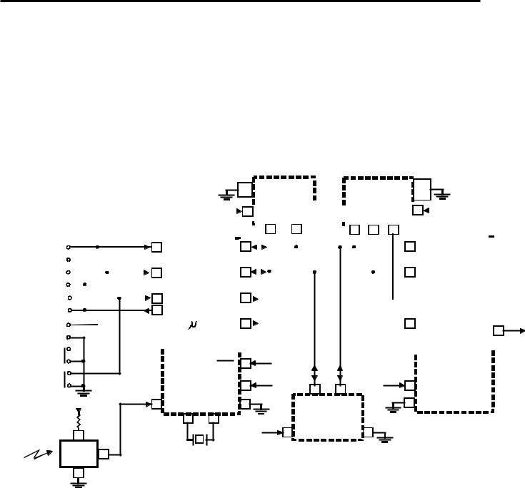
Figure 7, System Control Block Diagram
12 System Control
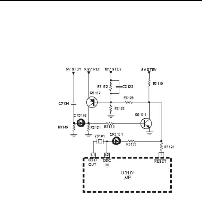
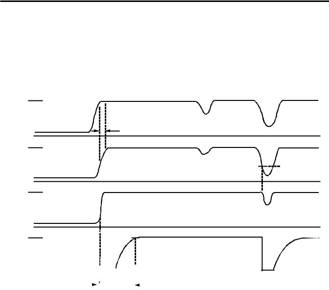
Reset Circuit The reset circuit starts the microprocessor at a known place in its program. U3101 reset is an active low to pin 1. When AC power is first applied, the reset circuit goes high after approximately 55msec. This allows the crystal oscillator time to come up and stabilize before allowing the microprocessor to run. The reset circuit also monitors the condition of the 12 volt standby supply. If the 12 volt standby supply drops below 10 volts, the reset circuit activates and puts the microprocessor in a low power mode.
Figure 8, Reset Circuit
A stable 5.6 volt reference is applied to the emitter of Q3102. The 12 volt standby supply is divided by R3132 and R3133 so approximately 6 volts is applied to the base of Q3102. The collector of Q3102 is tied to the base of Q3101. The collector of Q3101 is connected to the 5 volt standby supply and to the reset pin 1 of U3101. Under normal operating conditions, the voltage on the base of Q3102 is at 6 volts which is high enough to keep Q3102 off. If the 12 volt standby supply drops far enough to allow the voltage on the base of Q3102 to drop to 5 volts, Q3102 will turn on. When Q3102 turns
System Control 13
on, Q3101 will also turn on and disable the 5 volt reset line to ground initiating a reset to U3101. Q3101 also disables the crystal oscillator by grounding it through R3139 and CR3101. This places the microprocessor in a low power mode to maintain the nonvolatile memory.
120V
120VAC
10 mSEC APPROX.
12V
5V
2V STBY
5V
5V STBY #1
5V
RESET
|
|
|
|
|
|
|
|
|
|
|
(ACTIVE = 0) |
|
|
|
|
|
|
|
|
55 mSEC APPROX. |
|
|
|
|
|
|
|
|
|
|||
|
|
|
|
|
|
|
|
|||
Figure 9, Reset Circuit Timing
14 System Control
Data
Communications
Five IC’s make up the system control circuit: U3101, main microprocessor; U1001, T-Chip; U2901, D-PIP microprocessor; U3201, EEPROM; and U7401, tuner PLL(Phase Lock Loop). These IC’s communicate with U3101 via serial data lines. The format used to communicate is called “bus protocol.” Three bus protocols are used in this system: IM Bus, I2C Bus and the T-Bus. While it is not necessary for the technician to completely understand the individual protocols for troubleshooting the system control circuits, knowing what type of information is exchanged and what IC pins are involved will make troubleshooting more efficient and effective. All circuits in the CTC177 chassis family interface with the system control circuit in one form or another. It is important to decide whether the circuit itself is at fault or if the system control circuit is the problem.
1,2,3 |
GND U3201 |
U2901 GND |
3,5 |
15,16 |
|||
4,7 |
EEPROM |
D-PIP |
40,41 |
|
|||
|
|
|
|
|
|
|
|
|
|
|
|
|
|
|
|
|
|
|
|
|
|
|
|
|
5V |
|
|
8 |
|
|
|
|
|
|
|
|
|
|
|
|
|
|
|
|
|
|
|
|
|
|
|
|
|
|
|
|
|
|
|
VDD |
|
39 |
|
|
|
|
|
|
5V |
|
|||||||||||||||||||||||||||
|
|
|
|
|
|
|
|
|
|
|
|
|
|
|
|
|
|
|
|
|
|
|
|
|
VDD |
|
|
|
|
|
|
|
|
|
|
|
|
|
|
|
|
|
|
|
|
|
|
|
|
|
|
|
|
|
|
|
|
||||||||||||||||||||||||||||||||||||||
|
|
|
|
|
|
|
|
|
|
|
|
|
|
|
|
|
|
|
|
|
|
|
|
|
|
|
|
|
|
|
|
|
|
|
|
|
DATA |
|
|
CLOCK |
|
|
DATA CLOCK ENABLE |
|
|
|
|
|
|
|
|
|
|
|
|
|
|
|
|
|
|
|
|
|
|
|
|
||||||||||||||||||||||||||||
|
|
|
|
|
|
|
|
|
|
|
|
|
|
|
|
|
|
|
|
|
|
|
|
|
|
|
|
|
|
|
|
|
|
|
|
|
|
|
|
|
|
|
|
|
|
|
|
|
|
|
|
|
|
|
|
|
|
|
|
|
|
|
|
||||||||||||||||||||||||||||||||
|
|
|
|
|
|
|
|
|
|
|
|
|
|
|
|
|
|
|
|
|
|
|
|
|
|
|
|
|
|
|
|
|
|
|
|
|
|
|
|
|
|
|
|
|
|
|
|
|
|
|
|
|
|
|
|
|
|
|
|
|
|
|
|
|
|
|
|
|
|
|
|
|
|
|
|
|
|
|
|
|
|
|
|
|
|
|
|
|
|
|
|
|
|
||
|
|
|
|
|
|
|
|
|
|
|
|
|
|
|
|
|
|
|
|
|
|
|
|
|
|
|
|
|
|
|
|
|
|
|
|
|
|
|
5 |
|
|
|
|
|
|
6 |
|
|
|
20 |
21 |
|
22 |
|
|
|
|
|
|
|
|
|
|
|
|
|
|
|
|
|
|
|
|
|
|
|
|
|
|
|
|||||||||||||||
|
|
|
|
|
|
|
|
|
|
|
|
|
|
|
|
|
|
|
|
|
|
|
|
|
|
|
|
|
|
|
|
|
|
|
|
|
|
|
|
|
|
|
|
|
|
|
|
|
|
|
|
|
|
|
|
|
|
|
|
|
|
|
|
|
|
|
|
|
|
|
|
|
|
|
|
|
|
|
|
|
|
|
|
|
|
|
|
|
|
|
|
|
|
|
|
|
|
|
|
|
|
|
|
|
|
|
KS1 |
|
|
|
T-CHIP DATA |
|
15 |
|
|
|
|
|
|
|
|
|
|
|
|
|
|
|
|
|
|
|
|
|
|
|
|
|
|
|
|
|
|
|
|
|
|
|
|
|
|
|
|
|
|
|
|
|
|
|
|
|
|
|
|
|
|
|
|
|
|
|
|
|
|
||||||||||||||||
POWER |
|
|
|
6 |
|
|
|
|
|
|
|
|
TUNER CLOCK |
|
|
|
|
|
|
|
|
|
|
|
|
|
|
|
|
|
|
|
|
|
|
|
|
|
|
|
|
|
54 |
|
DATA |
|
|
|
|
|
|
|
|
|
|
|
|
|
|
||||||||||||||||||||||||||||||||||||
|
|
|
KS2 |
|
|
T-CHIP CLOCK |
|
16 |
|
|
|
|
|
|
|
|
|
|
|
|
|
|
|
|
|
|
|
|
|
|
|
|
|
|
|
|
|
|
|
|
|
|
|
|
53 |
|
CLOCK |
|
|
|
|
|
|
|
|
|
|
|
|
|
|
||||||||||||||||||||||||||||||||||
|
|
|
|
|
|
|
|
|
7 |
|
|
|
|
|
|
|
|
|
|
|
|
|
|
|
|
|
|
|
|
|
|
|
|
|
|
|
|
|
|
|
|
|
|
|
|
|
|
|
|
|
|
|
|
|
|
|
|
|
|
|
|
|
|
||||||||||||||||||||||||||||||||
VOL. UP |
|
|
|
|
|
|
|
|
|
|
|
|
|
|
|
|
TUNER DATA |
|
|
|
|
|
|
|
|
|
|
|
|
|
|
|
|
|
|
|
|
|
|
|
|
|
|
|
|
|
|
|
|
|
|
|
|
|
|
|
|
|
|
|
|
|
|
|
|
|
|
|
|
|
|
|
|
|
|
|
|||||||||||||||||||
|
|
|
|
|
|
|
|
|
|
8 |
KS3 |
|
|
|
|
|
|
|
|
|
|
PIP |
|
12 |
|
|
|
|
|
|
|
|
|
|
|
|
|
|
|
|
|
|
|
|
|
|
|
|
|
|
|
|
|
|
|
|
|
|
|
|
|
|
|
|
|
|
|
|
|
|
|
|
|
|
|
|
|
|
|
|
|
|
|
|
|
|
|||||||||
VOL. DN. |
|
|
|
|
|
|
|
KD1 |
|
|
|
|
|
|
|
|
ENABLE |
|
|
|
|
|
|
|
|
|
|
|
|
|
|
|
|
|
|
|
|
|
|
|
|
|
|
|
|
|
|
|
|
|
|
|
|
|
|
|
|
|
|
|
|
|
|
|
|
|
U1001 |
|
|||||||||||||||||||||||||||
|
|
|
|
|
|
5 |
U3101 |
T-CHIP |
|
|
|
|
|
|
|
|
|
|
|
|
|
|
|
|
|
|
|
|
|
|
|
|
|
|
|
|
|
|
|
|
|
|
|
|
|
|
|
|
|
|
|
|
|
|
|
|
|
|
T-CHIP |
|
|||||||||||||||||||||||||||||||||||
|
|
|
|
|
|
|
|
|
|
|
|
|
|
|
|
|
|
|
|
P |
|
|
|
|
|
|
14 |
|
|
|
|
|
|
|
|
|
|
|
|
|
|
|
|
|
|
|
|
|
|
|
|
|
|
|
|
|
|
|
|
|
|
|
|
52 |
|
ENABLE |
|
|
|
|
|
|
|
|
HORZ. |
|
|||||||||||||||||||
CH. UP |
|
|
|
|
|
|
|
|
|
|
|
|
|
|
|
|
|
|
|
ENABLE |
|
|
|
|
|
|
|
|
|
|
|
|
|
|
|
|
|
|
|
|
|
|
|
|
|
|
|
|
|
|
|
|
|
|
|
|
|
|
|
|
|
|
|
|
|
|
24 |
||||||||||||||||||||||||||||
|
|
|
|
|
|
|
|
|
|
|
|
|
|
|
|
|
|
|
|
|
|
|
|
|
|
|
|
|
|
|
|
|
|
|
|
|
|
|
|
|
|
|
|
|
|
|
|
|
|
|
|
|
|
|
|
|
|
|
|
|
|
|
|
|
|
|
|
|
|
|
|
|
|
|
|
|
|
|
|
|
|
|
OUT |
||||||||||||
|
|
|
|
|
|
|
|
|
|
|
|
|
|
|
|
|
|
|
|
|
|
|
|
|
|
|
|
|
|
|
|
|
|
|
|
|
|
|
|
|
|
|
|
|
|
|
|
|
|
|
|
|
|
|
|
|
|
|
|
|
|
|
|
|
|
|
|
|
|
|
|
|
|
|
|
|
|
|
|
|
|
|
|
|
|
|
|
|
|
|
|
|
|
|
|
CH. DN. |
|
|
|
|
1 |
5V |
|
|
|
|
|
|
|
|
RESET |
|
|
|
|
|
|||
MENU |
|
|
|
VDD |
20 |
5V |
|
|
7.6 V |
22 |
|
|
|
|
|
4 |
5 |
STBY |
|
||||
|
|
|
|
|
|
|
|||||
|
|
|
|
|
|
|
|
|
|||
5V |
3 |
OSC |
OSC |
GND |
21 |
|
DATA |
CLOCK |
|
56 |
BUS |
OUT |
IN |
|
U7401 |
|
GND |
||||||
|
|
|
|
|
|
|
|||||
|
|
41 |
42 |
|
|
|
TUNER PLL |
|
|
|
|
2 |
|
|
|
|
5V |
10 |
VCC |
GND 13 |
|
|
|
|
|
|
|
|
|
|
|
|
|
|
|
IR3401 |
1 |
Y3101 |
|
|
|
|
|
|
|
|
|
|
|
|
|
|
|
|
|
|
|
||
3 |
|
|
|
|
|
|
|
|
|
|
|
Figure 10, System Control Circuit (repeated)
IM Bus
The IM Bus is a three wire bus U3101 uses to communicate with the D-PIP microprocessor. Pins 15, 16 and 12 on U3101 are the IM Bus Data, Clock and PIP Enable lines. These are connected to pins 20, 21 and 22 respectively on U2901, the D-PIP microprocessor. When the PIP Enable line goes low, eight bits of address data synchronized to clock transitions are sent. Next, the Enable line goes high followed by eight bits of “Write” or “Read” information. The Enable line then momentarily goes low to signal the end of the transaction. Because the PIP Enable line and data protocol are unique to the PIP microprocessor, other devices that share the data and clock lines are unaffected by communications between U3101 and U2901.

System Control 15
I2C Bus
The I2C Bus is a two wire bus U3101 uses to communicate with the tuner PLL, U7401 and EEPROM, U3201. Pins 15 and 16 of U3101 are the clock and data lines for the I2C Bus. Notice this is reversed compared to the IM Bus. These pins are connected to pins 6 and 5 of U3201 and pins 5 and 4 of U7401 respectively. Data transfers are signaled when the data line goes LOW while the clock is HI. Eight bits of address data followed by an acknowledge bit are sent. Next, eight bits of Read/Write data followed by an acknowledge bit are sent. Because the data protocols are unique and the enable lines are not used, only I2C Bus devices respond to I2C Bus commands.
T-Bus
The T-Bus protocol is a three wire bus enabling U3101 to communicate with U1001. This bi-directional bus allows the microprocessor to control the operations within U1001 and allows U1001 to report operation status back.
|
|
|
|
|
START |
|
|
|
|
|
|
|
|
|
|
|
|
|
|
|
|
|
|
|
|
|
|
|
|
|
|
|
|
|
|
|
|
|
|
|
|
|
|
|
|
|
|
|
|
|
|
|
|
|
|
|
|
|
|
|
|
|
|
|
|
|
|
|
|
|
|
|
|
|
|
|
|
|
|
|
|
|
|
|
|
|
|
|
|
|
|
|
|
|
|
|
|
|
|
|
STOP |
||||||||||
|
CLOCK |
|
|
|
|
|
|
|
|
|
|
|
|
|
|
|
|
|
|
|
|
|
|
|
|
|
|
|
|
|
|
|
|
|
|
|
|
|
|
|
|
|
|
|
|
|
|
|
|
|
|
|
|
|
|
|
|
|
|
|
|
|
|
|
|
|
|
|
|
|
|
|
|
|
|
|
|
|
|
|
|
|
|
|
|
|
|
|
|
|
|
|
|
|
|
|
|
|
|
|
|
|
|
|
|
||||||
|
|
|
|
|
|
|
|
|
|
|
|
|
|
|
|
|
|
|
|
|
|
|
|
|
|
|
|
|
|
|
|
|
|
|
|
|
|
|
|
|
|
|
|
|
|
|
|
|
|
|
|
|
|
|
|
|
|
|
|
|
|
|
|
|
|
|
|
|
|
|
|
|
|
|
|
|
|
|
|
|
|
|
|
|
|
|
|
|
|
|
|
|
|
|
|
|
|
|
|
|
|
|
|
|
|
|
|
|
|
|
|
|
(SCL) |
|
|
|
|
|
|
|
|
|
|
|
|
|
|
|
|
|
|
|
|
|
|
|
|
|
|
|
|
|
|
|
|
|
|
|
|
|
|
|
|
|
|
|
|
|
|
|
|
|
|
|
|
|
|
|
|
|
|
|
|
|
|
|
|
|
|
|
|
|
|
|
|
|
|
|
|
|
|
|
|
|
|
|
|
|
|
|
|
|
|
|
|
|
|
|
|
|
|
|
|
|
|
|
|
|
|
|
|
|
|
I2 C |
|
|
|
|
|
|
|
|
|
|
|
|
|
|
|
|
|
|
|
|
|
|
|
|
|
|
|
|
|
|
|
|
|
|
|
|
|
|
|
|
|
|
|
|
|
|
|
|
|
|
|
|
|
|
|
|
|
|
|
|
|
|
|
|
|
|
|
|
|
|
|
|
|
|
|
|
|
|
|
|
|
|
|
|
|
|
|
|
|
|
|
|
|
|
|
|
|
|
|
|
|
|
|
|
|
|
|
|
|
|
|
|
|
|
|
|
|
|
|
|
|
|
|
|
|
|
|
|
|
|
|
|
|
|
|
|
|
|
|
|
|
|
|
|
|
|
|
|
|
|
|
|
|
|
|
|
|
|
|
|
|
|
|
|
|
|
|
|
|
|
|
|
|
|
|
|
|
|
|
|
|
|
|
|
|
|
|
|
|
|
|
|
|
|
|
|
|
|
|
|
|
|
|
|
|
|
|
|
|
|
|
|
|
|
|
|
|
|
|
|
|
|
|
BUS |
|
|
|
|
|
|
|
|
|
|
|
|
|
|
|
|
|
|
|
|
|
|
|
|
|
|
|
|
|
|
|
|
|
|
|
|
|
|
|
|
|
|
|
|
|
|
|
|
|
|
|
|
|
|
|
|
|
|
|
|
|
|
|
|
|
|
|
|
|
|
|
|
|
|
|
|
|
|
|
|
|
|
|
|
|
|
|
|
|
|
|
|
|
|
|
|
|
|
|
|
|
|
|
|
|
|
|
|
|
|
|
|
DATA |
|
|
|
|
|
|
|
|
|
|
|
|
|
|
|
|
|
|
|
|
|
|
|
|
|
|
|
|
|
|
|
|
|
|
|
|
|
|
|
|
|
|
|
|
|
|
|
|
|
|
|
|
|
|
|
|
|
|
|
|
|
|
|
(OPTIONAL DATA BYTES) |
|
|
|
|
|
|
|
|
|
|
|
|
|
|
|
|
|
|
|
|
|
|
|
|
|
|||||||||||||||||||||
|
(SDA) |
|
|
|
|
|
1 |
|
|
2 |
|
3 |
|
|
4 |
5 |
|
6 |
|
7 |
|
8 |
|
9 |
|
|
1 |
|
2 |
|
3 |
|
4 |
|
|
5 |
|
6 |
|
7 |
|
8 |
|
|
|
|
9 |
|
|
|
|
|
|
|
|
|
|
|
|
|
|
|
|
|
|
|
|
|
|
|
|
|
|
|
|
|
|
|
|
|
|
|
|
||||||||||||||||||||||||||||
|
|
|
|
|
|
|
|
|
|
|
|
|
|
|
|
|
|
|
|
|
|
|
|
|
|
|
|
|
|
|
|
|
|
|
|
|
|
|
|
|
|
|
|
|
|
|
|
|
|
|
|
|
|
|
|
|
|
|
|
|
|
|
|
|
|
|
|
|
|
|
|
|
|
|
|
|
|
|
|
|
|
|
|
|
|
||||||||||||||||||||||||||
|
|
|
|
|
|
|
|
|
|
|
|
|
ADDRESS |
|
|
|
|
|
|
ACK |
|
|
|
“WRITE” OR “READ” DATA |
|
ACK |
|
|
|
|
|
|
|
|
|
|
|
|
|
|
|
|
|
|
|
|
|
|
|
|
|
|
|
|
|
|
|
|
|
|
|
|
|
|
|
|
|
|
|
|
|
|
|
|
|
|
STOP |
||||||||||||||||||||||||||||||||||
|
|
|
|
|
|
|
|
|
|
|
|
|
|
|
|
|
|
|
|
|
|
|
|
|
|
|
|
|
|
|
|
|
|
|
|
|
|
|
|
|
|
|
|
|
|
|
|
|
|
|
|
|
|
|
|
|
|
|
|
|
|
|
|
|
|
|
|
|
|
|
|
|
|||||||||||||||||||||||||||||||||||||||
|
|
|
|
|
|
|
|
|
|
|
|
|
|
|
|
|
|
|
|
|
|
|
|
|
|
|
|
|
|
|
|
|
|
|
|
|
|
|
|
|
|
|
|
|
|
|
|
|
|
|
|
|
|
|
|
|
|
|
|
|
|
|
|
|
|
|
|
||||||||||||||||||||||||||||||||||||||||||||
|
|
|
|
|
START |
|
|
|
|
|
|
|
|
|
|
|
|
|
|
|
|
|
|
|
|
|
|
|
|
|
|
|
|
|
|
|
|
|
|
|
|
|
|
|
|
|
|
|
|
|
|
|
|
|
|
|
|
|
|
|
|
|
|
|
|
|
|
|
|
|
|
|
|
|
|
|
|
|
|
|
|
|
|
|
|
|
|
|
|
|
|
|
|
|
|
|
|
|
|
|
|||||||||||
IM |
ENABLE |
|
|
|
|
|
|
|
|
|
|
|
|
|
|
|
|
|
|
|
|
|
|
|
|
|
|
|
|
|
|
|
|
|
|
|
|
|
|
|
|
|
|
|
|
|
|
|
|
|
|
|
|
|
|
|
|
|
|
|
|
|
|
|
|
|
|
|
|
|
|
|
|
|
|
|
|
|
|
|
|
|
|
|
|
|
|
|
|
|
|
|
|
|
|
|
|
|
|
|
|
|
|
|
|
|
|
|
|
|
|
CLOCK |
|
|
|
|
|
|
|
|
|
|
|
|
|
|
|
|
|
|
|
|
|
|
|
|
|
|
|
|
|
|
|
|
|
|
|
|
|
|
|
|
|
|
|
|
|
|
|
|
|
|
|
|
|
|
|
|
|
|
|
|
|
|
|
|
|
|
|
|
|
|
|
|
|
|
|
|
|
|
|
|
|
|
|
|
|
|
|
|
|
|
|
|
|
|
|
|
|
|
|
|
|
|
|
|
|
|
|
|
|
|
|
|
|
|
|
|
|
|
|
|
|
|
|
|
|
|
|
|
|
|
|
|
|
|
|
|
|
|
|
|
|
|
|
|
|
|
|
|
|
|
|
|
|
|
|
|
|
|
|
|
|
|
|
|
|
|
|
|
|
|
|
|
|
|
|
|
|
|
|
|
|
|
|
|
|
|
|
|
|
|
|
|
|
|
|
|
|
|
|
|
|
|
|
|
|
|
|
|
|
|
|
|
|
|
|
|
|
|
|
|
|
||
BUS |
|
|
|
|
|
|
|
|
|
|
|
|
|
|
|
|
|
|
|
|
|
|
|
|
|
|
|
|
|
|
|
|
|
|
|
|
|
|
|
|
|
|
|
|
|
|
|
|
|
|
|
|
|
|
|
|
|
|
|
|
|
|
|
|
|
|
|
|
|
|
|
|
|
|
|
|
|
|
|
|
|
|
|
|
|
|
|
|
|
|
|
|
|
|
|
|
|
|
|
|
|
|
|
|
|
|
|
|
|
|
|
|
DATA |
|
|
|
|
|
|
|
|
|
|
|
|
|
|
|
|
|
|
|
|
|
|
|
|
|
|
|
|
|
|
|
|
|
|
|
|
|
|
|
|
|
|
|
|
|
|
|
|
|
|
|
|
|
|
|
|
|
|
|
|
|
|
|
|
|
|
|
|
|
|
|
|
|
|
|
|
|
|
|
|
|
|
|
|
|
|
|
|
|
|
|
|
|
|
|
|
|
|
|
|
|
|
|
|
|
|
|
|
|
|
|
|
|
|
|
|
|
|
|
|
|
|
|
|
|
|
|
|
|
|
|
|
|
|
|
|
|
|
|
|
|
|
|
|
|
|
|
|
|
|
|
|
|
|
|
|
|
|
|
|
|
|
|
|
|
|
|
|
|
|
|
|
|
|
|
|
|
|
|
|
|
|
|
|
|
|
|
|
|
|
|
|
|
|
|
|
|
|
|
|
|
|
|
|
|
|
|
|
|
|
|
|
|
|
|
|
|
|
|
|
|
|
|
|
|
|
1 |
|
|
2 |
3 |
|
|
4 |
5 |
|
6 |
7 |
8 |
|
|
|
|
1 |
|
2 |
3 |
|
4 |
|
|
5 |
|
7 |
8 |
|
|
|
|
|
|
|
|
|
|
|
|
|
|
|
|
|
|
(OPTIONAL DATA BYTES) |
|
|
|
|
|
|
|
|
|
|
|
|
|
|
|
|
|
|
|
|
|
|
|
|
|
|||||||||||||||||||||||||||||||||||
|
|
|
|
|
|
|
|
|
|
|
|
|
ADDRESS |
|
|
|
|
|
|
|
|
|
|
|
“WRITE” OR “READ” DATA |
|
|
|
|
|
|
|
|
|
|
|
|
|
|
|
|
|
|
|
|
|
|
|
|
|
|
|
|
|
|
|
|
|
|
|
|
|
|
|
|
|
|
|
|
|
|
|
|
|
|
|
|
|
|
|
|
|
OPTIONAL |
||||||||||||||||||||||||||||
|
|
|
|
|
|
|
|
|
|
|
|
|
|
|
|
|
|
|
|
|
|
|
|
|
|
|
|
|
|
|
|
|
|
|
|
|
|
|
|
|
|
|
|
|
|
|
|
|
|
|
|
|
|
|
|
|
|
|
|
|
|
|
|
|
|
|
|
|
|
|
|
|
|
|
|
|
|
|
|
|
|||||||||||||||||||||||||||||||
|
|
|
|
|
|
|
|
|
|
|
|
|
|
|
|
|
|
|
|
|
|
|
|
|
|
|
|
|
|
|
|
|
|
|
|
|
|
|
|
|
|
|
|
|
|
|
|
|
|
|
|
|
|
|
|
|
|
|
|
|
|
|
|
|
|
|
|
|
|
|
|
|
|
|
|
|
|
|
|
|
|||||||||||||||||||||||||||||||
|
|
|
|
|
|
|
|
|
|
|
|
|
|
|
|
|
|
|
|
|
|
|
|
|
|
|
|
|
|
|
|
|
|
|
|
|
|
|
|
|
|
|
|
|
|
|
|
|
|
|
|
|
|
|
|
|
|
|
|
|
|
|
|
|
|
|
|
|
|
|
|
|
|
|
|
|
|
|
|
|
|
|
|
|
|
|
|
|
|
|
|
|
|
|
|
|
|
|
|
|
|
|
|
|
|||||||
|
|
|
|
|
START |
|
|
|
|
|
|
|
|
|
|
|
|
|
|
|
|
|
|
|
|
|
|
|
|
|
|
|
|
|
|
|
|
|
|
|
|
|
|
|
|
|
|
|
|
|
|
|
|
|
|
|
|
|
|
|
|
|
|
|
|
|
|
|
|
|
|
|
|
|
|
|
|
|
|
|
|
|
|
|
|
|
|
|
|
|
|
|
|
|
|
|
|
|
|
|
STOP |
||||||||||
|
|
|
|
|
|
|
|
|
|
|
|
|
|
|
|
|
|
|
|
|
|
|
|
|
|
|
|
|
|
|
|
|
|
|
|
|
|
|
|
|
|
|
|
|
|
|
|
|
|
|
|
|
|
|
|
|
|
|
|
|
|
|
|
|
|
|
|
|
|
|
|
|
|
|
|
|
|
|
|
|
|
|
|
|
|
|
|
|
|
|
|
|
|
|
|
|
|
|
|
|
|
|
|
|
|
||||||
THOMSON |
ENABLE |
|
|
|
|
|
|
|
|
|
|
|
|
|
|
|
|
|
|
|
|
|
|
|
|
|
|
|
|
|
|
|
|
|
|
|
|
|
|
|
|
|
|
|
|
|
|
|
|
|
|
|
|
|
|
|
|
|
|
|
|
|
|
|
|
|
|
|
|
|
|
|
|
|
|
|
|
|
|
|
|
|
|
|
|
|
|
|
|
|
|
|
|
|
|
|
|
|
|
|
|
|
|
|
|
|
|
|
|
|
|
|
|
|
|
|
|
|
|
|
|
|
|
|
|
|
|
|
|
|
|
|
|
|
|
|
|
|
|
|
|
|
|
|
|
|
|
|
|
|
|
|
|
|
|
|
|
|
|
|
|
|
|
|
|
|
|
|
|
|
|
|
|
|
|
|
|
|
|
|
|
|
|
|
|
|
|
|
|
|
|
|
|
|
|
|
|
|
|
|
|
|
|
|
|
|
|
|
|
|
|
|
|
|
|
|
|
|
|
|
|
||
CLOCK |
|
|
|
|
|
|
|
|
|
|
|
|
|
|
|
|
|
|
|
|
|
|
|
|
|
|
|
|
|
|
|
|
|
|
|
|
|
|
|
|
|
|
|
|
|
|
|
|
|
|
|
|
|
|
|
|
|
|
|
|
|
|
|
|
|
|
|
|
|
|
|
|
|
|
|
|
|
|
|
|
|
|
|
|
|
|
|
|
|
|
|
|
|
|
|
|
|
|
|
|
|
|
|
|
|
|
|
|
|
|
|
|
|
|
|
|
|
|
|
|
|
|
|
|
|
|
|
|
|
|
|
|
|
|
|
|
|
|
|
|
|
|
|
|
|
|
|
|
|
|
|
|
|
|
|
|
|
|
|
|
|
|
|
|
|
|
|
|
|
|
|
|
|
|
|
|
|
|
|
|
|
|
|
|
|
|
|
|
|
|
|
|
|
|
|
|
|
|
|
|
|
|
|
|
|
|
|
|
|
|
|
|
|
|
|
|
|
|
|
|
|
||
BUS |
|
|
|
|
|
|
|
|
|
|
|
|
|
|
|
|
|
|
|
|
|
|
|
|
|
|
|
|
|
|
|
|
|
|
|
|
|
|
|
|
|
|
|
|
|
|
|
|
|
|
|
|
|
|
|
|
|
|
|
|
|
|
|
|
|
|
|
|
|
|
|
|
|
|
|
|
|
|
|
|
|
|
|
|
|
|
|
|
|
|
|
|
|
|
|
|
|
|
|
|
|
|
|
|
|
|
|
|
|
|
|
|
DATA |
|
|
|
|
|
|
|
|
|
|
|
|
|
|
|
|
|
|
|
|
|
|
|
|
|
|
|
|
|
|
|
|
|
|
|
|
|
|
|
|
|
|
|
|
|
|
|
|
|
|
|
|
|
|
|
|
|
|
|
|
|
|
|
|
|
|
|
|
|
|
|
|
|
|
|
|
|
|
|
|
|
|
|
|
|
|
|
|
|
|
|
|
|
|
|
|
|
|
|
|
|
|
|
|
|
|
|
|
|
|
|
|
|
|
|
|
|
|
|
|
|
|
|
|
|
|
|
|
|
|
|
|
|
|
|
|
|
|
|
|
|
|
|
|
|
|
|
|
|
|
|
|
|
|
|
|
|
|
|
|
|
|
|
|
|
|
|
|
|
|
|
|
|
|
|
|
|
|
|
|
|
|
|
|
|
|
|
|
|
|
|
|
|
|
|
|
|
|
|
|
|
|
|
|
|
|
|
|
|
|
|
|
|
|
|
|
|
|
|
|
|
|
|
|
|
|
|
|
1 |
|
|
2 |
|
3 |
|
|
4 |
|
5 |
|
6 |
|
7 |
|
8 |
|
|
|
|
1 |
|
2 |
3 |
|
4 |
|
5 |
|
6 |
|
7 |
8 |
|
|
|
|
|
|
|
|
|
1 |
|
2 |
|
3 |
|
4 |
|
5 |
6 |
|
7 |
|
8 |
|
|
|
|
|
1 |
|
2 |
|
3 |
|
4 |
|
5 |
|
6 |
|
7 |
|
8 |
|
|
|
|
|
||||||||||||||||||||||||
|
|
|
|
|
|
|
|
|
|
|
|
|
|
|
|
|
|
|
|
|
|
|
|
|
|
|
|
|
|
|
|
|
|
|
|
|
|
|
|
|
|
|
|
||||||||||||||||||||||||||||||||||||||||||||||||||||||||||||||||||||
|
|
|
|
|
|
|
|
|
|
|
|
|
ADDRESS |
|
|
|
|
|
|
|
|
|
|
|
|
|
“WRITE” DATA |
|
|
|
|
|
|
|
|
|
|
|
|
|
|
|
|
|
|
|
|
|
|
|
|
|
|
|
“READ” DATA (2 BYTES) |
|
|
|
|
|
|
|
|
|
|
|
|
|
|
|
|
|
|
|
|||||||||||||||||||||||||||||||||||||
|
|
|
|
|
|
|
|
|
|
|
|
|
|
|
|
|
|
|
|
|
|
|
|
|
|
|
|
|
|
|
|
|
|
|
|
|
|
|
|
|
|
|
|
|
|
|
|
|
|
|
|
|
|
|
|
|
|
|
|
|
|
|
|
|
|
|
|
|
|
|
|
||||||||||||||||||||||||||||||||||||||||
|
|
|
|
|
|
|
|
|
|
|
|
|
|
|
|
|
|
|
|
|
|
|
|
|
|
|
|
|
|
|
|
|
|
|
|
|
|
|
|
|
|
|
|
|
|
|
|
|
|
|
|
|
|
|
|
|
|
|
|
|
|
|
|
|
|
|
|
|
|
|
|
||||||||||||||||||||||||||||||||||||||||
|
|
|
|
|
|
|
|
|
|
|
|
|
|
|
|
|
|
|
|
|
|
|
|
|
|
|
|
|
|
|
|
|
|
|
|
|
|
|
|
|
|
|
|
|
|
|
|
|
|
|
|
|
|
|
|
|
|
|
|
|
|
|
|
|
|
|
|
|
|
|
|
|
|
|
|
|
|
|
|
|
|
|
|
|
|
|
|
|
|
|
|
|
|
|
|
|
|
|
|
|
|
|
|
|
|
|
|
|
|
|
|
Figure 11, Bus Protocols

16 System Control
Two distinct sections of a T-Bus transaction are called Read and Write. During the Write portion, the microprocessor drives the DATA line to send new register information to U1001. During the Read portion, U1001 drives the DATA line to transfer status information to the microprocessor, U3101.
The Write portion of the transaction is 16 bits long consisting of an IC Address (4 bits), Subaddress (5 bits) and Data field (7 bits). The Address identifies U1001. The Subaddress indicates the register inside U1001 and the Data is the value of the information being sent to U1001 by U3101. The Write portion of the transaction begins when U3101 pulls the ENABLE line low. Once the ENABLE line is low, the microprocessor must drive the DATA line one bit at a time while toggling the clock line. U1001 accepts data on the rising edge of the clock pulse.
|
|
|
|
START |
|
|
|
|
|
|
|
|
|
|
|
|
|
|
|
|
|
|
|
|
|
|
|
|
|
|
|
|
|
|
|
|
|
|
|
|
|
|
|
|
|
|
|
|
|
|
|
|
|
|
|
|
|
|
|
|
|
|
|
|
|
|
|
|
|
|
|
|
|
|
|
|
STOP |
||||||||||
|
CLOCK |
|
|
|
|
|
|
|
|
|
|
|
|
|
|
|
|
|
|
|
|
|
|
|
|
|
|
|
|
|
|
|
|
|
|
|
|
|
|
|
|
|
|
|
|
|
|
|
|
|
|
|
|
|
|
|
|
|
|
|
|
|
|
|
|
|
|
|
|
|
|
|
|
|
|
|
|
|
|
|
|
|
|
|
|
|
|
|
(SCL) |
|
|
|
|
|
|
|
|
|
|
|
|
|
|
|
|
|
|
|
|
|
|
|
|
|
|
|
|
|
|
|
|
|
|
|
|
|
|
|
|
|
|
|
|
|
|
|
|
|
|
|
|
|
|
|
|
|
|
|
|
|
|
|
|
|
|
|
|
|
|
|
|
|
|
|
|
|
|
|
|
|
|
|
|
|
|
I2 C |
|
|
|
|
|
|
|
|
|
|
|
|
|
|
|
|
|
|
|
|
|
|
|
|
|
|
|
|
|
|
|
|
|
|
|
|
|
|
|
|
|
|
|
|
|
|
|
|
|
|
|
|
|
|
|
|
|
|
|
|
|
|
|
|
|
|
|
|
|
|
|
|
|
|
|
|
|
|
|
|
|
|
|
|
|
|
|
|
|
|
|
|
|
|
|
|
|
|
|
|
|
|
|
|
|
|
|
|
|
|
|
|
|
|
|
|
|
|
|
|
|
|
|
|
|
|
|
|
|
|
|
|
|
|
|
|
|
|
|
|
|
|
|
|
|
|
|
|
|
|
|
|
|
|
|
|
|
|
|
|
|
|
|
|
|
|
|
|
|
|
|
|
|
|
|
BUS |
|
|
|
|
|
|
|
|
|
|
|
|
|
|
|
|
|
|
|
|
|
|
|
|
|
|
|
|
|
|
|
|
|
|
|
|
|
|
|
|
|
|
|
|
|
|
|
|
|
|
|
|
|
|
|
|
|
|
|
|
|
|
|
|
|
|
|
|
|
|
|
|
|
|
|
|
|
|
|
|
|
|
|
|
|
|
|
|
DATA |
|
|
|
|
|
|
|
|
|
|
|
|
|
|
|
|
|
|
|
|
|
|
|
|
|
|
|
|
|
|
|
|
|
|
|
|
|
|
|
|
|
|
|
|
|
|
|
|
|
|
|
|
|
|
|
|
|
|
|
|
(OPTIONAL DATA BYTES) |
|
|
|
||||||||||||||||||||||
|
(SDA) |
|
|
|
|
|
1 |
|
|
2 |
|
3 |
|
|
4 |
|
|
5 |
|
|
6 |
|
7 |
|
8 |
|
9 |
|
|
1 |
|
2 |
|
3 |
|
4 |
|
5 |
|
6 |
|
7 |
|
8 |
9 |
|
|
|
|
|
|
|
|
|
|
||||||||||||||||||||||||||||||||
|
|
|
|
|
|
|
|
|
|
|
|
|
|
|
|
|
|
|
|
|
|
|
|
|
|
|
|
|
|
|
|
|
|
|
|
|
|
|
|
|
|
|
|
|
|
|
|
|
|
|
|
|
|
|
|
|
|
|
|
||||||||||||||||||||||||||||
|
|
|
|
|
|
|
|
|
|
|
|
|
|
ADDRESS |
|
|
|
|
|
|
|
ACK |
|
|
|
|
“WRITE” OR “READ” DATA |
|
ACK |
|
|
|
|
|
|
|
|
|
|
|
|
|
|
|
|
|
|
|
|
|
|
|
|
|
|
|
STOP |
||||||||||||||||||||||||||||||
|
|
|
|
|
|
|
|
|
|
|
|
|
|
|
|
|
|
|
|
|
|
|
|
|
|
|
|
|
|
|
|
|
|
|
|
|
|
|
|
|
|
|
|
|
|
|
|
|
|
|
|
|
|||||||||||||||||||||||||||||||||||
|
|
|
|
|
|
|
|
|
|
|
|
|
|
|
|
|
|
|
|
|
|
|
|
|
|
|
|
|
|
|
|
|
|
|
|
|
|
|
|
|
|
|
|
|
|
|
|
|
|
||||||||||||||||||||||||||||||||||||||
|
|
|
|
|
START |
|
|
|
|
|
|
|
|
|
|
|
|
|
|
|
|
|
|
|
|
|
|
|
|
|
|
|
|
|
|
|
|
|
|
|
|
|
|
|
|
|
|
|
|
|
|
|
|
|
|
|
|
|
|
|
|
|
|
|
|
|
|
|
|
|
|
|
|
|
|
|
|
|
|||||||||
IM |
ENABLE |
|
|
|
|
|
|
|
|
|
|
|
|
|
|
|
|
|
|
|
|
|
|
|
|
|
|
|
|
|
|
|
|
|
|
|
|
|
|
|
|
|
|
|
|
|
|
|
|
|
|
|
|
|
|
|
|
|
|
|
|
|
|
|
|
|
|
|
|
|
|
|
|
|
|
|
|
|
|
|
|
|
|
|
|
|
|
CLOCK |
|
|
|
|
|
|
|
|
|
|
|
|
|
|
|
|
|
|
|
|
|
|
|
|
|
|
|
|
|
|
|
|
|
|
|
|
|
|
|
|
|
|
|
|
|
|
|
|
|
|
|
|
|
|
|
|
|
|
|
|
|
|
|
|
|
|
|
|
|
|
|
|
|
|
|
|
|
|
|
|
|
|
|
|
|
|
|
|
|
|
|
|
|
|
|
|
|
|
|
|
|
|
|
|
|
|
|
|
|
|
|
|
|
|
|
|
|
|
|
|
|
|
|
|
|
|
|
|
|
|
|
|
|
|
|
|
|
|
|
|
|
|
|
|
|
|
|
|
|
|
|
|
|
|
|
|
|
|
|
|
|
|
|
|
|
|
|
|
|
|
|
|
|
||
BUS |
|
|
|
|
|
|
|
|
|
|
|
|
|
|
|
|
|
|
|
|
|
|
|
|
|
|
|
|
|
|
|
|
|
|
|
|
|
|
|
|
|
|
|
|
|
|
|
|
|
|
|
|
|
|
|
|
|
|
|
|
|
|
|
|
|
|
|
|
|
|
|
|
|
|
|
|
|
|
|
|
|
|
|
|
|
|
|
|
DATA |
|
|
|
|
|
|
|
|
|
|
|
|
|
|
|
|
|
|
|
|
|
|
|
|
|
|
|
|
|
|
|
|
|
|
|
|
|
|
|
|
|
|
|
|
|
|
|
|
|
|
|
|
|
|
|
|
|
|
|
|
|
|
|
|
|
|
|
|
|
|
|
|
|
|
|
|
|
|
|
|
|
|
|
|
|
|
|
|
|
|
|
|
|
|
|
|
|
|
|
|
|
|
|
|
|
|
|
|
|
|
|
|
|
|
|
|
|
|
|
|
|
|
|
|
|
|
|
|
|
|
|
|
|
|
|
|
|
|
|
|
|
|
|
|
|
|
|
|
|
|
|
|
|
|
|
|
|
|
|
|
|
|
|
|
|
|
|
|
|
|
|
|
|
|
|
|
|
1 |
|
|
2 |
3 |
|
|
4 |
|
|
5 |
|
|
6 |
7 |
8 |
|
|
|
|
1 |
|
2 |
3 |
4 |
5 |
6 |
7 |
|
8 |
|
|
|
|
|
|
|
|
|
(OPTIONAL DATA BYTES) |
|||||||||||||||||||||||||||||||||||||||||||||
|
|
|
|
|
|
|
|
|
|
|
|
|
|
ADDRESS |
|
|
|
|
|
|
|
|
|
|
|
|
|
“WRITE” OR “READ” DATA |
|
|
|
|
|
|
|
|
|
|
|
|
|
|
|
|
|
|
|
|
|
|
|
|
|
|
|
|
|
|
|
|
|
|
|
|
|||||||||||||||||||||||
|
|
|
|
|
|
|
|
|
|
|
|
|
|
|
|
|
|
|
|
|
|
|
|
|
|
|
|
|
|
|
|
|
|
|
|
|
|
|
|
|
|
|
|
|
|
|
|
|
|
|
|
|
|
|
|
|
|
|
|
|
|
|
|||||||||||||||||||||||||
|
|
|
|
|
|
|
|
|
|
|
|
|
|
|
|
|
|
|
|
|
|
|
|
|
|
|
|
|
|
|
|
|
|
|
|
|
|
|
|
|
|
|
|
|
|
|
|
|
|
|
|
|
|
|
|
|
|
|
|
|
|
|
|||||||||||||||||||||||||
OPTIONAL
STOP
START
THOMSON |
ENABLE |
|
|
|
|
|
|
|
|
|
|
|
|
|
|
|
|
|
|
|
|
|
|
|
|
|
|
|
|
|
|
|
|
|
|
|
|
|
|
|
|
|
|
|
|
|
|
|
|
|
|
|
|
|
|
|
|
|
|
|
|
|
|
|
|
|
|
|
|
|
|
|
|
|
|
|
|
|
|
|
|
|
|
|
|
|
|
|
|
||
CLOCK |
|
|
|
|
|
|
|
|
|
|
|
|
|
|
|
|
|
|
|
|
|
|
|
|
|
|
|
|
|
|
|
|
|
|
|
|
|
|
|
|
|
|
|
|
|
|
|
|
|
|
|
|
|
|
|
|
|
|
|
|
|
|
|
|
|
|
|
|
|
|
|
|
|
|
|
|
|
|
|
|
|
|
|
|
|
|
|
|
|
|
|
|
|
|
|
|
|
|
|
|
|
|
|
|
|
|
|
|
|
|
|
|
|
|
|
|
|
|
|
|
|
|
|
|
|
|
|
|
|
|
|
|
|
|
|
|
|
|
|
|
|
|
|
|
|
|
|
|
|
|
|
|
|
|
|
|
|
|
|
|
|
|
|
|
|
|
|
|
|
|
|
|
|
|
|
|
|
|
|
|
|
||
BUS |
|
|
|
|
|
|
|
|
|
|
|
|
|
|
|
|
|
|
|
|
|
|
|
|
|
|
|
|
|
|
|
|
|
|
|
|
|
|
|
|
|
|
|
|
|
|
|
|
|
|
|
|
|
|
|
|
|
|
|
|
|
|
|
|
|
|
|
|
|
|
|
|
|
|
|
|
|
|
|
|
|
|
|
|
|
|
|
|
|
|
|
|
DATA |
|
|
|
|
|
|
|
|
|
|
|
|
|
|
|
|
|
|
|
|
|
|
|
|
|
|
|
|
|
|
|
|
|
|
|
|
|
|
|
|
|
|
|
|
|
|
|
|
|
|
|
|
|
|
|
|
|
|
|
|
|
|
|
|
|
|
|
|
|
|
|
|
|
|
|
|
|
|
|
|
|
|
|
|
|
|
|
|
|
|
|
|
|
|
|
|
|
|
|
|
|
|
|
|
|
|
|
|
|
|
|
|
|
|
|
|
|
|
|
|
|
|
|
|
|
|
|
|
|
|
|
|
|
|
|
|
|
|
|
|
|
|
|
|
|
|
|
|
|
|
|
|
|
|
|
|
|
|
|
|
|
|
|
|
|
|
|
|
|
|
|
|
|
|
|
|
|
|
|
|
||
|
|
|
|
1 |
2 |
3 |
4 |
|
5 |
|
|
6 |
7 |
8 |
|
|
1 |
2 |
3 |
4 |
5 |
6 |
|
7 |
8 |
|
|
|
1 |
|
2 |
|
3 |
|
4 |
|
5 |
|
6 |
|
7 |
|
8 |
|
|
|
1 |
|
2 |
|
3 |
|
4 |
|
5 |
|
6 |
|
7 |
|
8 |
|
|
|
|||||||||||||||||||||||||||
|
|
|
|
|
|
|
|
|
|
|
|
|
|
|
|
|
|
|
|
|
|
|
|
|
|
|
|
|
|
|
|
|
|||||||||||||||||||||||||||||||||||||||||||||||||||||||||||
|
|
|
|
|
|
|
|
|
|
|
ADDRESS |
|
|
|
|
|
|
|
|
|
|
|
|
|
“WRITE” DATA |
|
|
|
|
|
|
|
|
|
|
|
|
|
|
|
|
|
|
|
“READ” DATA (2 BYTES) |
|
|
|
|
|
|
|
|
|
|
|
|
|
|
|
|
|
|
|
|||||||||||||||||||||||||||
|
|
|
|
|
|
|
|
|
|
|
|
|
|
|
|
|
|
|
|
|
|
|
|
|
|
|
|
|
|
|
|
|
|
|
|
|
|
|
|
|
|
|
|
|
|
|
|
|
|
|
|
|
|
|
|
|
|
|
|
|
|
||||||||||||||||||||||||||||||
|
|
|
|
|
|
|
|
|
|
|
|
|
|
|
|
|
|
|
|
|
|
|
|
|
|
|
|
|
|
|
|
|
|
|
|
|
|
|
|
|
|
|
|
|
|
|
|
|
|
|
|
|
|
|
|
|
|
|
|
|
|
||||||||||||||||||||||||||||||
|
|
|
|
|
|
|
|
|
|
|
|
|
|
|
|
|
|
|
|
|
|
|
|
|
|
|
|
|
|
|
|
|
|
|
|
|
|
|
|
|
|
|
|
|
|
|
|
|
|
|
|
|
|
|
|
|
|
|
|
|
|
|
|
|
|
|
|
|
|
|
|
|
|
|
|
|
|
|
|
|
|
|
|
|
|
|
|
|
|
|
|
Figure 12, Bus Protocols (repeated)
After the Write portion of the transaction is completed, the Read portion begins. The Read portion is the answer back to U3101 from U1001. It too is 16 bits long consisting of Acknowledge (4 bits), Status (4 bits) and Data (8 bits). The Acknowledge bits let U3101 know it did in fact access U1001. The Status bits S0 through S3 inform U3101 of operating conditions in U1001:

System Control 17
S0 - Power-ON-Reset (POR)
S1 - X-ray Protection Fault (XRP)
S2 - Horizontal Lock Detector
S3 - Delayed Transfer Complete (BID)
The last 8 bits of the Read portion contain the Digital AFT information from the IF. This information is only looked at during channel change.
POR (Power-ON-Reset)
U1001 has a standby power monitor called POR. This circuit detects when the Standby Vcc has dropped below approximately 6 volts and shuts the IC off by stopping both the PWM and horizontal outputs. The output of the POR circuit is available to U3101 as one bit every T-Bus transaction.
The POR circuit output is latched and reset on the OFF to ON transition of the ON/ OFF bit. This means when the TV is ON and a standby transient occurs that triggers the POR circuit, it is necessary to send an OFF command followed by an ON command to get the set started again. If the Standby Vcc is still too low when an ON command is received, the IC will stay in the OFF mode requiring the process to be repeated.
XRP
The XRP bit in the status portion of the T-Bus transaction informs U3101 if an XRP condition has occurred. When the XRP input is above the reference value, the comparator’s output will turn the TV off by stopping both the PWM and Horizontal outputs.
The XRP bit is latched internally and gets reset at the ON to OFF transition of the ON/ OFF bit. This means to restart the TV after an XRP trip, the microprocessor must first send an OFF command followed by an ON command.
When the ON/OFF bit is in the OFF state, the XRP latch is disabled internally. This means for U3101 to read the valid state of the XRP detector, it is necessary for the ON/ OFF bit to be in the ON state.
Horizontal Lock Detector
This detector compares the position of the flyback pulse with the sync of the selected video source. This output is available to the microprocessor as a bit on the Read portion of every T-Bus transaction. While this detector can be used to detect the presence of an active channel, it is not used for tuning. A separate sync pulse input is applied to pin 39 of U3101 for that purpose.
The horizontal lock detector is used for detecting whether or not an active video source is connected to the composite or s-video input jacks. When s-video or composite video is selected, U3101 selects the video source and looks at the horizontal lock bit. If lock is detected, the source appears on the screen. If no lock is detected, U3101 displays “UNUSABLE SIGNAL” on the screen.

18 System Control
The horizontal lock bit also informs U3101 whether or not to select s-video or composite video. When “00” is entered to select a video source, U3101 first selects s-video and checks for a lock. If no lock occurs, composite video is selected.
Delayed Transfer Mode (BID)
Power-On
Sequence
This bit is used in transferring of data to the T-Chip registers. It is currently not used.
U3101 does not have a single on/off control pin to turn the television on or off as in previous chassis. The T-Chip is controlled entirely via the serial bus. Power on/off commands are accomplished by U3101 telling U1001 to turn on horizontal drive by means of a data command. U1001 contains its own standby 7.6 volt regulator to keep data communications alive and the horizontal drive stage operative while the set is off (Standby Mode). When the On command is received and horizontal drive is established, run supplies come up and bias the rest of U1001’s circuits bringing the set into the full on mode. An Off command from U3101 will cause horizontal drive to cease resulting in the scan derived supplies turning off. This removes power to the other circuits associated with U1001, placing the set in the standby mode.
1,2,3 |
GND U3201 |
U2901 GND |
3,5 |
15,16 |
|||
4,7 |
EEPROM |
D-PIP |
40,41 |
|
|
|
|
|
|
|
|
|
|
|
|
|
|
|
|
|
|
|
|
5V |
|
|
8 |
|
|
|
|
|
|
|
|
|
|
|
|
|
|
|
|
|
|
|
|
|
|
|
|
|
|
|
|
|
|
VDD |
|
39 |
|
|
|
|
|
|
5V |
|||||||||||||||||||||||||
|
|
|
|
|
|
|
|
|
|
|
|
|
|
|
|
|
|
|
|
VDD |
|
|
|
|
|
|
|
|
|
|
|
|
|
|
|
|
|
|
|
|
|
|
|
|
|
|
|
|
|
|
||||||||||||||||||||||||||||||||||||
|
|
|
|
|
|
|
|
|
|
|
|
|
|
|
|
|
|
|
|
|
|
|
|
|
|
|
|
|
|
|
DATA |
|
|
CLOCK |
|
|
DATA CLOCK ENABLE |
|
|
|
|
|
|
|
|
|
|
|
|
|
|
|
|
|
|
|
|
|
|
|||||||||||||||||||||||||||
|
|
|
|
|
|
|
|
|
|
|
|
|
|
|
|
|
|
|
|
|
|
|
|
|
|
|
|
|
|
|
|
|
|
|
|
|
|
|
|
|
|
|
|
|
|
|
|
|
|
|
|
|
|
|
|
|||||||||||||||||||||||||||||||
|
|
|
|
|
|
|
|
|
|
|
|
|
|
|
|
|
|
|
|
|
|
|
|
|
|
|
|
|
|
|
|
|
|
|
|
|
|
|
|
|
|
|
|
|
|
|
|
|
|
|
|
|
|
|
|
|
|
|
|
|
|
|
|
|
|
|
|
|
|
|
|
|
|
|
|
|
|
|
|
|
|
|
|
|
|
|
|
|
|
|
|
|
|
|
|
|
|
|
|
|
|
|
|
|
|
|
|
|
|
|
|
|
|
|
5 |
|
|
6 |
|
|
|
|
20 |
|
|
|
21 |
|
|
22 |
|
|
|
|
|
|
|
|
|
|
|
|
|
|
|
|
|
|
|
|
|
|
|
|
|
|
|
||||||||||||||||
|
|
|
|
|
|
|
|
|
|
|
|
|
|
|
|
|
|
|
|
|
|
|
|
|
|
|
|
|
|
|
|
|
|
|
|
|
|
|
|
|
|
|
|
|
|
|
|
|
|
|
|
|
|
|
|
|
|
|
|
|
|
|
|
|
|
|
|
|
|
|
|
|
|
|
|
|
|
|
|
|
|
|
|
|
|
|
|
|
|
|
|
|
KS1 |
|
T-CHIP DATA |
15 |
|
|
|
|
|
|
|
|
|
|
|
|
|
|
|
|
|
|
|
|
|
|
|
|
|
|
|
|
|
|
|
|
|
|
|
|
|
|
|
|
|
|
|
|
|
|
|
|
|
|
|
|
|
|
|
|
|
|
|
||||||||||||||||||
POWER |
6 |
|
|
|
|
|
|
|
|
TUNER CLOCK |
|
|
|
|
|
|
|
|
|
|
|
|
|
|
|
|
|
|
|
|
|
|
|
|
|
|
|
|
54 |
DATA |
|
|
|
|
|
|
|
|
|
|
|
|
||||||||||||||||||||||||||||||||||
|
|
|
|
|
7 |
KS2 |
T-CHIP CLOCK |
16 |
|
|
|
|
|
|
|
|
|
|
|
|
|
|
|
|
|
|
|
|
|
|
|
|
|
|
|
|
|
|
|
|
|
|
53 |
CLOCK |
|
|
|
|
|
|
|
|
|
|
|
|
||||||||||||||||||||||||||||||
|
|
|
|
|
|
|
|
|
|
|
|
|
|
|
|
|
|
|
|
|
|
|
|
|
|
|
|
|
|
|
|
|
|
|
|
|
|
|
|
|
|
|
|
|
|
|
|
|
|
|
||||||||||||||||||||||||||||||||||||
VOL. UP |
|
|
|
|
|
|
|
|
|
|
|
|
TUNER DATA |
|
|
|
|
|
|
|
|
|
|
|
|
|
|
|
|
|
|
|
|
|
|
|
|
|
|
|
|
|
|
|
|
|
|
|
|
|
|
|
|
|
|
|
|
|
|
|
|
|
|
|
|
|
|
|||||||||||||||||||
|
8 |
KS3 |
PIP |
12 |
|
|
|
|
|
|
|
|
VOL. DN. |
ENABLE |
|
|
|
|
|
|
U1001 |
|
|||
5 |
KD1 |
|
|
|
|
|
|
|
|
|
||
|
|
|
|
|
|
|
|
T-CHIP |
|
|||
|
|
U3101 T-CHIP |
|
|
|
|
|
52 |
|
|||
CH. UP |
|
P |
ENABLE 14 |
|
|
|
|
ENABLE |
HORZ. |
24 |
||
|
|
|
|
|
|
|
|
|
|
OUT |
||
CH. DN. |
|
|
RESET |
1 |
5V |
|
|
|
|
|
|
|
|
|
|
|
|
|
|
|
|
|
|||
MENU |
|
|
VDD |
20 |
5V |
|
|
7.6 V |
22 |
|
|
|
|
|
|
4 |
5 |
STBY |
|
|
|
||||
|
|
|
|
|
|
|
|
|||||
|
|
|
|
|
|
|
|
|
|
|||
5V |
|
OSC |
OSC |
21 |
|
DATA |
CLOCK |
|
56 |
BUS |
|
|
3 |
OUT |
IN GND |
|
U7401 |
|
GND |
|
|
||||
|
|
|
|
|
|
|
|
|||||
|
|
41 |
42 |
|
|
TUNER PLL |
|
|
|
|
|
|
2 |
|
|
|
5V |
10 |
VCC |
GND 13 |
|
|
|
|
|
|
|
|
|
|
|
|
|
|
|
|
|
|
IR3401 |
1 |
Y3101 |
|
|
|
|
|
|
|
|
|
|
|
|
|
|
|
|
|
|
|
|
|
||
3 |
|
|
|
|
|
|
|
|
|
|
|
|
Figure 13, System Control Circuit (repeated)
System Control 19
U3201 is the Electrically Erasable Programmable Read-Only Memory and uses the I2C Bus DATA and CLOCK lines to communicate with U3101. It provides non-volatile memory for storing the following:
•Channel Scan List
•Customer Features
•Chassis Alignments
•CRT Alignments
•DPIP Alignments
•Tuner Alignments
•Channel Labels
U3201 - EEPROM
If for any reason the EEPROM is replaced, the television will have to be completely realigned to store the correct alignment data in the new chip. For this reason, it is important not to change U3201 unless it is absolutely necessary.
TECH
TIP
The keyboard interface is very similar to those used in the past. An important difference is only one key drive line, KD1, is used. POWER, VOL. UP and VOL. DN. are driven by KD1. When one of these buttons is pressed, KD1 pulses the corresponding sense line low. U3101 detects which button has been pressed by monitoring the sense lines for the KD1 pulse. The other three switches pull KS1, KS2 and KS3 to ground. When U3101 sees a constant LO instead of a HI to LO pulse, it knows one of the other three buttons has been pressed and will initiate the appropriate function based on which sense line is pulled low.
Keyboard
Interface
Infrared remote signals are amplified by IR3401 and appear at U3101 pin 3 as 5 Vpp
data pulses. When no IR is received, the DC level at U3101 pin 3 is 5 volts. IR3401 IR Input is powered by the 5 volt standby supply.
C2707
Q2701
+


41  GRN OSD IN
. SYNC |
|
GRN OSD |
|
18 |
|
|
|
C2709 |
|
|
BLU OSD |
|
|||
|
OUT |
|
|
|
|
|
|
+ |
42 |
|
|
||||
|
24 |
|
|
|
|
|
|
|
|
|
|
IN |
|
||
V. SYNC |
25 |
U3101 |
U1001 |
|
Micro |
T-CHIP |
|
|
|
|
Figure 14, Non-Closed Caption, Early Production OSD Circuit
Two OSD circuits are used in the CTC177 chassis family. Early production televisions that do not support a closed caption decoder have a cyan OSD. Later production sets that include a closed caption decoder have a full color OSD.
On Screen
Display
20 System Control
Early production sets with a cyan display use only one OSD line out of U3101 to drive the green and blue OSD input on U1001. The OSD is produced in U3101 and is output from pin 18. Q2701 buffers the signal and capacitively couples it to the green and blue input on U1001 pins 41 and 42. Green and blue are driven equally resulting in the cyan display.
Later production sets that support closed caption decoders use red, green and blue outputs from U3101 (pins 19, 18 and 17) to drive the red, green and blue OSD inputs on U1001 (pins 40, 41 and 42) producing a full color OSD. Q2702, Q2701 and Q2703 buffer the red, green and blue signals and capacitively couple them to pins 40, 41 and 42 of U1001 respectfully.
Horizontal and vertical sync are input to pins 24 and 25 of U3101 and are used to control the position of the OSD on the screen.
+7.6
|
|
|
|
|
|
|
|
|
|
|
|
|
|
|
|
|
|
|
|
|
|
|
|
|
|
Q2701 |
|
|
|
|
|||||
|
|
|
|
|
|
|
|
|
|
|
|
|
GRN OSD |
|
18 |
|
|
|
|
||||||||||||||||
|
|
|
|
|
|
|
|
|
|
|
|
|
|
|
|
|
|
||||||||||||||||||
|
|
|
|
|
|
|
|
|
|
|
|
|
|
|
|
|
|
|
|
|
|
|
|
||||||||||||
|
|
|
|
|
|
|
|
|
|
|
|
|
|
|
|
|
|
|
|
|
|
|
|
||||||||||||
H. SYNC |
|
|
|
|
|
|
|
|
|
|
|
OUT |
|
|
|
|
|
|
|
|
|
|
|
|
|||||||||||
|
|
|
|
24 |
|
|
|
|
|
|
|
|
|
|
|
|
|
|
|
|
|
|
|
|
|
|
|
|
|
|
|
|
|
|
|
|
|
|
|
|
|
|
|
|
|
|
U3101 |
|
+7.6 |
|
|||||||||||||||||||||
|
|
|
|
|
|
|
|
|
|
|
|
||||||||||||||||||||||||
V. SYNC |
|
|
|
|
|
|
|
|
P |
|
|
Q2703 |
|
|
|
||||||||||||||||||||
|
|
|
|
|
|
|
|
|
|
|
|
|
|||||||||||||||||||||||
|
|
|
|
|
|
|
|
|
|
|
|
|
|
|
|
|
|
|
|
|
|
|
|
||||||||||||
|
|
25 |
|
|
|
|
|
|
|
|
BLU OSD |
|
|
|
|
|
|
|
|
|
|
|
|
||||||||||||
CC. VIDEO |
|
|
|
|
|
|
|
|
|
|
OUT |
|
17 |
|
|
|
|
|
|
|
|
|
|
||||||||||||
|
|
|
|
|
|
|
|
|
|
|
|
|
|
|
|
|
|
|
|
|
|
|
|
|
|
|
|
|
|
|
|||||
|
|
|
|
|
|
|
|
|
|
|
|
|
|
|
|
|
|
|
|
|
|
|
|
|
|
|
|
|
|
|
|||||
|
|
|
|
|
|
|
|
|
|
|
|
|
|
|
|
|
|
|
|
|
|
|
|
|
|
|
|
|
|
|
|||||
|
|
|
|
|
|
|
|
|
|
|
|
|
|
|
|
|
|
|
|
+7.6 |
|||||||||||||||
13 |
|
|
|
|
|
|
|
|
|
|
|
|
|
|
|
|
|
|
|
|
|||||||||||||||
|
|
|
|
|
|
|
|
|
|
|
|
|
|
|
|
|
|
|
|
|
|
|
|
|
|
|
|
|
|
|
|
|
|
|
|
|
|
|
|
|
|
|
|
|
|
|
|
|
|
|
|
|
|
|
|
|
|
|
|
|
|
|
|
|
|
|
|
|
|
|
|
|
|
|
|
|
|
|
|
|
|
|
|
|
|
|
|
|
|
|
|
|
|
|
|
|
|
|
|
|
|
|
|
|
|
|
|
|
|
|
|
|
|
|
|
|
|
|
|
|
|
|
|
|
|
|
|
|
|
|
|
|
|
|
|
|
|
|
|
|
|
|
|
Q2702
RED OSD
OUT 
 19
19
C2707
+ |
41 |
GRN OSD |
|
|
|
IN |
|
|
|
|
|
|
|
|
|
|
|
|
|
|
|
|
|
|
|
|
|
|
|
|
|
|
|
|
|
|
|
|
|
|
|
|
|
|
|
|
|
U1001
T-CHIP
C2709 |
|
BLU OSD |
|
|
|
|
|||
|
|
|
|
|
|
+ |
42 |
IN |
|
|
|
|
|
|
|
|
|
|
|
|
|
|
|
|
|
|
|
|
|
|
|
|
|
|
|
|
|
|
|
|
|
|
|
|
|
|
|
|
|
|
|
|
|
|
|
|
|
|
|
|
|
|
|
|
|
|
|
|
|
|
|
|
|
|
|
|
|
|
|
|
|
|
|
|
|
|
|
|
|
C2708
|
+ |
40 |
RED OSD |
|
|||
|
|
|
IN
Closed
Caption
Figure 15, Closed Caption OSD Circuit
U3101 contains a closed caption decoder that interprets the closed caption data sent on line 21 of the first field in each frame of video. Sets that support the closed caption feature, video is input to pin 13 of U3101. The closed caption signal begins with a seven cycle burst of pulses to synchronize the decoder’s data clock. This is followed by a start bit followed by two eight-bit words consisting of seven bits of data followed by a parity bit for error correction. Since two characters are sent on line 21 of the first field of each frame, there are a total of 60 characters per second. This format sends two data channels called C1 and C2 (caption channel 1 and caption channel 2). Channel 1 is used for the main captioning text while channel 2 is used for alternate text, such as a second language or abbreviated captioning for children or slow readers. C1 and C2 are selectable from the menu; however, the TV will default to C1 each time the TV is unplugged for prolonged periods of time.

System Control 21
All closed caption processing is performed inside U3101. Horizontal and vertical sync at pins 24 and 25 of U3101 are also used by the closed caption decoder.
H SYNC |
COLOR BURST |
CLOCK RUN-IN |
START BITS |
|
|
|
|
CHARACTER ONE |
|
|
|
|
|
|
|
|
CHARACTER TWO |
|
|
|
|
||||||||||||||||
|
|
|
S1 |
|
S2 |
|
S3 |
B0 |
|
B1 |
|
B2 |
|
B3 |
|
B4 |
|
B5 |
|
B6 |
|
P1 |
B0 |
|
B1 |
|
B2 |
|
B3 |
|
B4 |
|
B5 |
|
B6 |
|
P2 |
|
|
|
|
|
|
|
|
|
|
|
|
|
|
|
|
|
|
|
|||||||||||||||||||
|
|
|
|
|
|
|
|
|
|
|
|
|
|
|
|
|
|
|
|
|
|
|
|
|
|
|
|
|
|
|
|
|
|
|
|
|
|
50
25
0
-40
IRE
Figure 16, Line 21 Closed Caption Signal
The service menu provides a method for instrument alignment and setup. This mode Service |
||
is accessed by pressing two combinations of buttons on the front panel keyboard. With |
Menu |
|
the instrument on, press and hold the menu button and then simultaneously press the |
||
|
||
power button. While continuing to hold the menu button, release the power button and |
|
|
then press the volume + button. The instrument should immediately display a one line |
|
|
menu on the screen: |
|
|
PARAMETER |
VALUE |
|
CONTROLLED |
||
CONTROLLED |
||
BY CHANNEL |
||
BY VOLUME +/- |
||
|
||
P 00 |
V 00 |
Figure 16, Service Menu
The decimal value on the left is the parameter number and the decimal value on the right is the current value of that parameter. Channel up and down increment and decrement the parameter number. Volume + / - adjust the current value of that parameter. Three parameters are used for security purposes to protect the factory alignments from being modified by the customer. The first security parameter, 00, requires a specific value to be selected with the volume +/- buttons before other parameters may be selected. If channel up/down is pressed without the correct security pass-number set, the service mode is exited. There are three main groups of parameters: instrument parameters, chassis parameters, and tuner parameters. The chassis and tuner parameters are each preceded by a security pass-number parameter to make changes very deliberate.

22 System Control
Most of the instrument and chassis parameters correspond to individual (unpacked) register fields in the T-chip. When these parameters are modified, the T-chip and the corresponding EEPROM location is updated.
The Menu button may be used to enable the vertical collapse setup line - it functions as a toggle. This setup line has the following characteristics:
S-video source is automatically selected (make sure no signal is connected to the S-video input)
Contrast is set to minimum
Brightness is set to 7.5 IRE
Vertical kill enabled
When the setup line is toggled off, the characteristics modified above return to their prior settings except contrast which is set to the factory default. Changing to another parameter (with channel up/down) also toggles off the setup line.
The tuner parameters correspond to the three alignments for each of 19 channels for a total of 57 parameters. When these parameters are modified, the tuner D/A and the EEPROM are updated. Note that you must manually select the proper channel for each tuner alignment. These adjustments may be made from the front panel as well as the remote. The digit entry buttons (on the remote) allow tuning to any channel in this mode. Pressing the power on, off, or power toggle buttons exits this service mode.

System Control 23
Alignment
Parameters

24 System Control

System Control 25
The system control circuit controls every function of the TV. A failure in this circuit System Control
will cause the entire TV to malfunction. Because U3101 and U1001 are so interrelated, Troubleshooting there is a lot of overlapping in troubleshooting procedures. A failure of U3101, U1001,
U3201, U2901 or U7401 can make the television completely inoperative. It is important to follow a systematic isolation approach to localize the problem. Because U3101 turns the TV ON via a serial data bus command to U1001, a failure in the system
control circuit can result in a DEAD SET condition.
DIGITAL
1,2,3 |
GND U3201 |
U2901 GND |
3,5 |
15,16 |
|||
4,7 |
EEPROM |
D-PIP |
40,41 |
|
|
|
|
|
|
|
|
|
|
|
|
|
|
|
|
|
|
|
|
|
|
|
|
|
5V |
|
|
|
8 |
|
|
|
|
|
|
|
|
|
|
|
|
|
|
|
|
|
|
|
|
|
|
|
|
|
|
|
|
|
|
|
|
VDD |
|
39 |
|
|
|
|
|
|
5V |
|
||||||||||||||||||||||||||
|
|
|
|
|
|
|
|
|
|
|
|
|
|
|
|
|
|
|
|
|
|
|
|
|
|
|
VDD |
|
|
|
|
|
|
|
|
|
|
|
|
|
|
|
|
|
|
|
|
|
|
|
|
|
|
|
|
|
|
|
|
|||||||||||||||||||||||||||||||||||||
|
|
|
|
|
|
|
|
|
|
|
|
|
|
|
|
|
|
|
|
|
|
|
|
|
|
|
|
|
|
|
|
|
|
|
|
|
|
DATA |
|
|
CLOCK |
|
|
DATA CLOCK ENABLE |
|
|
|
|
|
|
|
|
|
|
|
|
|
|
|
|
|
|
|
|
|
|
|
|
||||||||||||||||||||||||||||
|
|
|
|
|
|
|
|
|
|
|
|
|
|
|
|
|
|
|
|
|
|
|
|
|
|
|
|
|
|
|
|
|
|
|
|
|
|
|
|
|
|
|
|
|
|
|
|
|
|
|
|
|
|
|
|
|
|
|
|
|
|
|
|
|
||||||||||||||||||||||||||||||||
|
|
|
|
|
|
|
|
|
|
|
|
|
|
|
|
|
|
|
|
|
|
|
|
|
|
|
|
|
|
|
|
|
|
|
|
|
|
|
|
|
|
|
|
|
|
|
|
|
|
|
|
|
|
|
|
|
|
|
|
|
|
|
|
|
|
|
|
|
|
|
|
|
|
|
|
|
|
|
|
|
|
|
|
|
|
|
|
|
|
|
|
|
|
|||
|
|
|
|
|
|
|
|
|
|
|
|
|
|
|
|
|
|
|
|
|
|
|
|
|
|
|
|
|
|
|
|
|
|
|
|
|
|
|
|
5 |
|
|
|
|
|
|
6 |
|
|
|
20 |
21 |
|
22 |
|
|
|
|
|
|
|
|
|
|
|
|
|
|
|
|
|
|
|
|
|
|
|
|
|
|
|
|||||||||||||||
|
|
|
|
|
|
|
|
|
|
|
|
|
|
|
|
|
|
|
|
|
|
|
|
|
|
|
|
|
|
|
|
|
|
|
|
|
|
|
|
|
|
|
|
|
|
|
|
|
|
|
|
|
|
|
|
|
|
|
|
|
|
|
|
|
|
|
|
|
|
|
|
|
|
|
|
|
|
|
|
|
|
|
|
|
|
|
|
|
|
|
|
|
|
|
|
|
|
|
|
|
|
|
|
|
|
|
|
KS1 |
|
|
|
T-CHIP DATA |
|
15 |
|
|
|
|
|
|
|
|
|
|
|
|
|
|
|
|
|
|
|
|
|
|
|
|
|
|
|
|
|
|
|
|
|
|
|
|
|
|
|
|
|
|
|
|
|
|
|
|
|
|
|
|
|
|
|
|
|
|
|
|
|
|
|
||||||||||||||||
POWER |
|
|
|
6 |
|
|
|
|
|
|
|
|
TUNER CLOCK |
|
|
|
|
|
|
|
|
|
|
|
|
|
|
|
|
|
|
|
|
|
|
|
|
|
|
|
|
|
|
54 |
|
DATA |
|
|
|
|
|
|
|
|
|
|
|
|
|
|
||||||||||||||||||||||||||||||||||||
|
|
|
KS2 |
|
|
T-CHIP CLOCK |
|
16 |
|
|
|
|
|
|
|
|
|
|
|
|
|
|
|
|
|
|
|
|
|
|
|
|
|
|
|
|
|
|
|
|
|
|
|
|
|
53 |
|
CLOCK |
|
|
|
|
|
|
|
|
|
|
|
|
|
|
||||||||||||||||||||||||||||||||||
|
|
|
|
|
|
|
|
|
7 |
|
|
|
|
|
|
|
|
|
|
|
|
|
|
|
|
|
|
|
|
|
|
|
|
|
|
|
|
|
|
|
|
|
|
|
|
|
|
|
|
|
|
|
|
|
|
|
|
|
|
|
|
|
|
|
||||||||||||||||||||||||||||||||
|
|
|
|
|
|
|
|
|
|
|
|
|
|
|
|
|
|
|
|
|
|
|
|
|
|
|
|
|
|
|
|
|
|
|
|
|
|
|
|
|
|
|
|
|
|
|
|
|
|
|
|
|
|
|
|
|
|
|
|
|
|
|
|
|||||||||||||||||||||||||||||||||
VOL. UP |
|
|
|
|
|
|
|
|
|
|
|
|
|
|
|
|
TUNER DATA |
|
|
|
|
|
|
|
|
|
|
|
|
|
|
|
|
|
|
|
|
|
|
|
|
|
|
|
|
|
|
|
|
|
|
|
|
|
|
|
|
|
|
|
|
|
|
|
|
|
|
|
|
|
|
|
|
|
|
|
|
|||||||||||||||||||
|
|
|
|
|
|
|
|
|
|
8 |
KS3 |
|
|
|
|
|
|
|
|
|
|
PIP |
|
12 |
|
|
|
|
|
|
|
|
|
|
|
|
|
|
|
|
|
|
|
|
|
|
|
|
|
|
|
|
|
|
|
|
|
|
|
|
|
|
|
|
|
|
|
|
|
|
|
|
|
|
|
|
|
|
|
|
|
|
|
|
|
|
|
|||||||||
VOL. DN. |
|
|
|
|
|
|
|
KD1 |
|
|
|
|
|
|
|
|
ENABLE |
|
|
|
|
|
|
|
|
|
|
|
|
|
|
|
|
|
|
|
|
|
|
|
|
|
|
|
|
|
|
|
|
|
|
|
|
|
|
|
|
|
|
|
|
|
|
|
|
|
|
U1001 |
|
|||||||||||||||||||||||||||
|
|
|
|
|
|
5 |
U3101 |
T-CHIP |
|
|
|
|
|
|
|
|
|
|
|
|
|
|
|
|
|
|
|
|
|
|
|
|
|
|
|
|
|
|
|
|
|
|
|
|
|
|
|
|
|
|
|
|
|
|
|
|
|
|
|
T-CHIP |
|
|||||||||||||||||||||||||||||||||||
CH. UP |
|
|
|
|
|
|
|
|
|
|
|
|
|
|
|
|
|
|
|
P |
ENABLE |
|
14 |
|
|
|
|
|
|
|
|
|
|
|
|
|
|
|
|
|
|
|
|
|
|
|
|
|
|
|
|
|
|
|
|
|
|
|
|
|
52 |
|
ENABLE |
|
|
|
|
|
|
|
|
HORZ. |
24 |
|||||||||||||||||||||||
|
|
|
|
|
|
|
|
|
|
|
|
|
|
|
|
|
|
|
|
|
|
|
|
|
|
|
|
|
|
|
|
|
|
|
|
|
|
|
|
|
|
|
|
|
|
|
|
|
|
|
|
|
|
|
|
|
|
|
|
|
|
|
|
|
|
|
|
|
|
|
|
|
|
|
|
|
|
|
|
|
|
|
|
OUT |
||||||||||||
|
|
|
|
|
|
|
|
|
|
|
|
|
|
|
|
|
|
|
|
|
|
|
|
|
|
|
|
|
|
|
|
|
|
|
|
|
|
|
|
|
|
|
|
|
|
|
|
|
|
|
|
|
|
|
|
|
|
|
|
|
|
|
|
|
|
|
|
|
|
|
|
|
|
|
|
|
|
|
|
|
|
|
|
|
|
|
|
|
|
|
|
|
|
|
|
|
CH. DN. |
|
|
|
|
|
5V |
|
|
|
|
|
|
|
|
RESET |
1 |
|
|
|
|
|
||
MENU |
|
|
|
VDD |
20 |
5V |
|
|
7.6 V |
22 |
|
|
|
|
|
4 |
5 |
STBY |
|
||||
|
|
|
|
|
|
|
|||||
|
|
|
|
|
|
|
|
|
|||
5V |
3 |
OSC |
OSC |
GND |
21 |
|
DATA |
CLOCK |
|
56 |
BUS |
OUT |
IN |
|
U7401 |
|
GND |
||||||
|
|
|
|
|
|
|
|||||
|
|
41 |
42 |
|
|
|
TUNER PLL |
|
|
|
|
2 |
|
|
|
|
5V |
10 |
VCC |
GND 13 |
|
|
|
|
|
|
|
|
|
|
|
|
|
|
|
IR3401 |
1 |
Y3101 |
|
|
|
|
|
|
|
|
|
|
|
|
|
|
|
|
|
|
|
||
3
Figure 17, System Control Circuit (repeated)
Dead Set
1.Make sure the standby power supplies are working. (12, 7.6 & 5)
2.Check for horizontal drive pulses out of pin 24 of U1001 when the power button is pressed. If the pulses are there even momentarily, system control is working and the problem is in the deflection circuits. If the pulses do not appear, check the 7.6 volt standby voltage on pin 22 of U1001. If the supply is not present on pin 22, unsolder the pin and see if the supply comes up on the pad. If it does, U1001 is defective. If it does not, trace the supply back to its source. If 7.6 volts is present on U1001 pin 22 in circuit, go to the next step.
26 System Control
TECH
TIP
TECH
TIP
3.Check for standby 5 volts on pin 20 of U3101. If it is missing, check the power supply. If present, go to the next step.
4.Check the reset pin 1 of U3101 for 5 volts. If it is low or missing, check the reset circuit. If it is, go to the next step.
5.Check pins 41 and 42 of U3101 for a 5 Vpp oscillator. If the signal is not 5 Vpp, check Y3101 and its peripheral components. If the signal is completely absent, suspect U3101 or Y3101. If the 4 MHz signal is present, go to the next step.
6.Monitor pins 14, 15 and 16 of U3101. There should be no data activity in the standby mode. When the power button is pressed, 5 Vpp data pulses should appear. If no pulses appear when the power button is pressed, unsolder pins 20, 21 and 22 of U2901 and pins 4 and 5 of U7401. Now re-check U3101 pins 14, 15 and 16. If data activity returns, suspect a defect in U2901’s or U7401’s circuit areas. If data activity does not return, go to the next step.
7.Unsolder pins 14, 15 and 16 on U3101 and check for constant 5 Vpp data pulses in the standby mode on those pins.
Note: When U3101 is initialized, it checks to see if U3201 is present. Under normal conditions, it immediately finds U3201 and ceases data activity . With the enable, data and clock lines disconnected, U3101 continues to send out data activity looking for U3201. This is normal and indicates U3101 is working.
If no data activity is seen on U3101 pins 14, 15 and 16 with the pins out of circuit, U3101 is probably defective. If data activity is present, reconnect the pins and go to the next step.
8.Having confirmed data activity on pins 14, 15 and 16 of U3101 out of circuit, disconnect pins 5 and 6 of U3201. Check for data activity in the standby mode on the circuit board foil side of U3201 pins 5 and 6. If data activity is present on the foil pads for those pins with the IC out of circuit, U3201 is defective.
Do not throw away the original U3201 until the problem is absolutely
confirmed. If U3201 turns out not to be the problem, putting the old IC back in will prevent a complete chassis alignment from having to be performed.
If no data activity is seen on the circuit board with U3201 out of circuit, connect the IC and go to the next step.
9.Unsolder pins 52, 53 and 54 on U1001. Check to see if the data pulses are present on the foil that leads to the pins. If data pulses are present on the circuit board foil, U1001 is most likely defective. If no data pulses appear on circuit board foil side of U1001 pins 52, 53 and 54, suspect an open connection or resistor, or possibly a leaky capacitor on the data bus.

System Control 27
10.Once the problem is isolated and repaired, do not forget to re-connect U2901, U7401 and any other parts that may have been unsoldered during troubleshooting.
|
1,2,3 |
GND U3201 |
|
U2901 GND |
3,5 |
|
||
|
|
15,16 |
|
|||||
|
4,7 |
EEPROM |
|
D-PIP |
40,41 |
|
||
5V |
|
|
|
5V |
||||
8 |
VDD |
|
|
|
VDD |
39 |
||
|
|
DATA |
CLOCK |
DATA CLOCK ENABLE |
|
|
||
|
|
5 |
6 |
20 |
21 |
22 |
|
|
|
|
|
|
|
|
|
|
|
|
|
|
|
|
|
|
|
|
|
|
|
|
|
|
|
|
|
|
|
|
|
|
|
|
|
|
|
|
|
|
|
|
|
|
|
|
|
|
|
|
|
|
|
|
|
|
|
|
|
|
|
|
|
|
|
|
|
|
|
|
KS1 |
|
|
|
T-CHIP DATA |
|
15 |
|
|
|
|
|
|
|
|
|
|
|
|
|
|
|
|
|
|
|
|
|
|
|
|
|
|
|
|
|||||||||||||||
POWER |
|
|
6 |
|
|
|
|
|
|
|
|
TUNER CLOCK |
|
|
|
54 |
|
DATA |
|
|
|
|
|
|
|
|
|
|
|
|
|
|
|||||||||||||||||||||||||||
|
|
|
KS2 |
|
|
T-CHIP CLOCK |
|
16 |
|
|
|
|
|
53 |
|
CLOCK |
|
|
|
|
|
|
|
|
|
|
|
|
|
|
|||||||||||||||||||||||||||||
|
|
|
|
|
|
|
|
7 |
|
|
|
|
|
|
|
|
|
|
|
|
|
|
|
|
|
|
|
|
|
|
|
||||||||||||||||||||||||||||
VOL. UP |
|
|
|
|
|
|
|
|
|
|
|
|
|
|
|
TUNER DATA |
|
|
|
|
|
|
|
|
|
|
|
|
|
|
|
|
|
|
|
|
|
|
|
|
|
|
|
|
|
|
|||||||||||||
|
|
|
|
|
|
|
|
|
8 |
KS3 |
|
|
|
|
|
|
|
|
|
|
PIP |
|
12 |
|
|
|
|
|
|
|
|
|
|
|
|
|
|
|
|
|
|
|
|
|
|
|
|
|
|
|
|
||||||||
VOL. DN. |
|
|
|
|
|
|
|
|
|
|
|
|
|
|
|
ENABLE |
|
|
|
|
|
|
|
|
|
|
|
|
|
|
|
U1001 |
|
||||||||||||||||||||||||||
|
|
|
5 |
KD1 |
|
|
|
|
|
|
|
|
|
|
|
|
|
|
|
|
|
|
|
|
|
|
|
|
|
|
|
|
|
|
|
||||||||||||||||||||||||
|
|
|
|
|
|
|
|
|
|
|
|
|
|
|
|
U3101 T-CHIP |
|
14 |
|
|
|
|
|
52 |
|
|
|
|
|
|
T-CHIP |
|
|||||||||||||||||||||||||||
CH. UP |
|
|
|
|
|
|
|
|
|
|
|
|
|
|
|
|
|
|
P ENABLE |
|
|
|
|
|
|
|
ENABLE |
|
|
|
|
|
|
|
|
HORZ. |
24 |
||||||||||||||||||||||
|
|
|
|
|
|
|
|
|
|
|
|
|
|
|
|
|
|
|
|
|
|
|
|
|
|
|
|
|
|
|
|
|
|
|
|
|
|
|
|
|
|
|
|
|
|
|
OUT |
||||||||||||
|
|
|
|
|
|
|
|
|
|
|
|
|
|
|
|
|
|
|
|
|
|
|
|
|
|
|
|
|
|
|
|
|
|
|
|
|
|
|
|
|
|
|
|
|
|
|
|
|
|
|
|
|
|
|
|
|
|
|
|
CH. DN. |
|
|
|
|
1 |
5V |
|
|
|
|
|
|
|
|
RESET |
|
|
|
|
|
|||
MENU |
|
|
|
VDD |
20 |
5V |
|
|
7.6 V |
22 |
|
|
|
|
|
4 |
5 |
STBY |
|
||||
|
|
|
|
|
|
|
|||||
|
|
|
|
|
|
|
|
|
|||
5V |
3 |
OSC |
OSC |
GND |
21 |
|
DATA |
CLOCK |
|
56 |
BUS |
OUT |
IN |
|
U7401 |
|
GND |
||||||
|
|
|
|
|
|
|
|
|
|
||
|
|
41 |
42 |
|
|
|
TUNER PLL |
|
|
|
|
2 |
|
|
|
|
5V |
10 |
VCC |
GND 13 |
|
|
|
|
|
|
|
|
|
|
|
|
|
|
|
IR3401 |
1 |
Y3101 |
|
|
|
|
|
|
|
|
|
|
|
|
|
|
|
|
|
|
|
||
3 |
|
|
|
|
|
|
|
|
|
|
|
Figure 18, System Control Circuit (Repeated)
 Loading...