


PCG-V505DC1x
Table of contents
 Loading...
Sony PCG-V505DC1x, PCG-V505DC1Px, PCG-V505W, PCG-V505T3x, PCG-V505DH Service Manual
...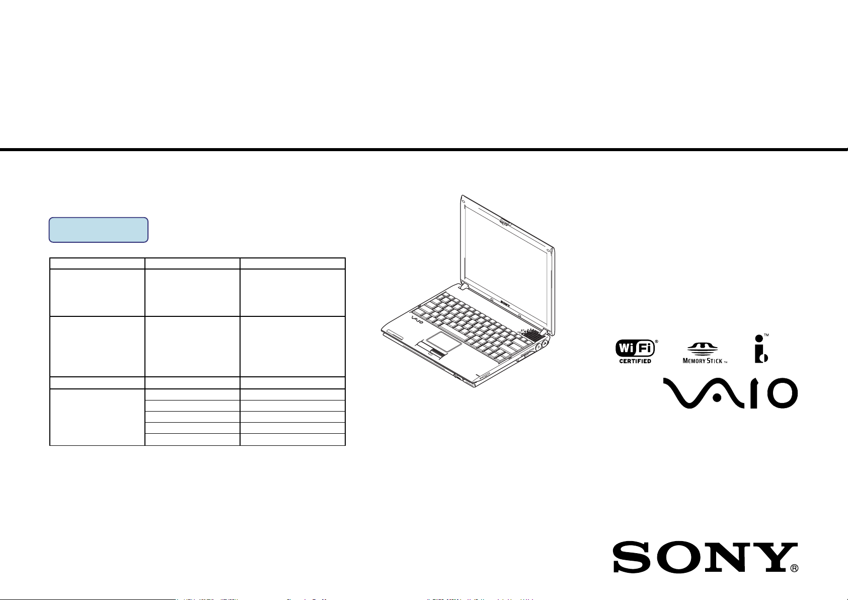
PCG-V505DC1x/V505DC1Px/V505DH/V505DX/V505DXP
Area Model Lineup
PCG-V505F/B
PCG-V505T3/Px∗
PCG-V505T3x∗
PCG-V505W/P
PCG-V505DC1x∗
PCG-V505DC1Px∗
PCG-V505DH
PCG-V505DX
PCG-V505DXP
European
AEP/UK
PCG-V505CP
Chinese PCG-V505MCP
Korean PCG-V505MLP
International PCG-V505MP
Thai PCG-V505MSP
Taiwan PCG-V505MTP
∗ : CTO Model
Asian/Oceania/
South Africa
PCG-V505MCP/V505MP/V505MLP/V505MSP/V505MTP
SERVICE MANUAL
Ver. 4 2003K
Revision History
Japanese Japanese
PCG-V505F/V505T3x/V505W
PCG-V505CP
American US Canadian
9-876-349-04
Confidential
• Design and specifications are subject to
change without notice.
本機の仕様および外観は、改良のため予告なく変更
•
することがあります が 、ご了承ください。
NOTEBOOK COMPUTER
S400
Information in this document is subject to
change without notice.
Sony, VAIO and CLIE are trademarks or registered trademarks of Sony. Microsoft,Windows,
Windows Media, Outlook, Bookshelf and other
Microsoft products are trademarks or registered
trademarks of Microsoft Corporation in the
United States and other countries.The word
Bluetooth and the Bluetooth logo are trademarks
of Bluetooth SIG, Inc. AMD, AMD logo, AMD
Duron and combinations there of, 3DNow!, are
trademarks of Adv anced Micro Devices, Inc. Intel
Inside logo, Pentium and Celeron are trademarks
or registered trademarks of Intel Corporation.
Transmeta, the Transmeta logo, Crusoe Processor, the Crusoe logo and combinations there of
are trademarks of Transmeta Corporation in the
USA and other countries. Graffiti, HotSync,
PalmModem, and Palm OS are resistered trademarks, and the Hotsync logo and Palm are trademarks of Palm,Inc. or its subsidiaries. (M) and
Motrola are trademarks of Motrora, Inc. Other
Motrola products and services with (R) mark like
Dragomball are the trademarks of Motrola, Inc.
All other names of systems, products and
servicesin this manual are trademarks or registered trademarks of their respective owners. In
this manual, the (TM) or (R) mark are not specified.
Caution Markings for Lithium/Ion Battery - The
following or similar texts shall be provided on
battery pack of equipment or in both the operating and the service instructions.
CAUTION: Danger of explosion if battery is incorrectly replaced. Replace only with the same
or equivalent type recommended by the manufacturer. Discard used batteries according to the
manufacturer’s instructions.
CAUTION: The battery pack used in this device
may present a fire or chemical burn hazard if
mistreated. Do not disassemble, heat above
100ºC (212ºF) or incinerate. Dispose of used battery promptly. Keep away from children.
CAUTION: Changing the back up battery.
•Overcharging, short circuiting, reverse charging, multilati on or incineration of the cells must
be avoided to prevent one or more of the following occurrences; release of toxic materials,
release of hydrogen and/or oxygen gas, rise in
surface temperature.
• If a cell has leaked or vented, it should be replaced immediately while avoiding to touch it
without any protection.
Service and Inspection Precautions
1. Obey precautionary markings and
instructions
Labels and stamps on the cabinet, chassis, and
components identify are as requiring special precautions. Be sure to observe these precautions,
as well as all precautions listed in the operating
manual and other associated documents.
2. Use designated parts only
The set’s components possess important safety
characteristics, such as noncombustibility and the
ability to tolerate large voltages. Be sure that replacement parts possess the same safety characteristics as the originals. Also remember that the
0 mark, which appears in circuit diagrams and
parts lists, denotes components that have particularly important safety functions; be extra sure to
use only the designated components.
3. Always follow the original
designwhen mounting parts and
routing wires
The original layout includes various safety features, such as inclusion of insulating materials
(tubes and tape) and the mounting of parts above
the printer board. In addition, internal wiring has
been routed and clamped so as to keep it away
from hot or high-voltage parts. When mounting
parts or routing wires, therefore, be sure
toduplicate the original layout.
– 2 –
4. Inspect after completing service
After servicing, inspect to make sure that all
screws, components, and wiring have been returned to their original condition. Also check the
area around the repair location to ensure that repair work has caused no damage, and confirm
safety.
5. When replacing chip components...
Never reuse components. Also remember that
the negative side of tantalum capacitors is easily
damaged by heat.
6. When handling flexible print
boards...
• The temperature of the soldering-iron tip
should be about 270ºC.
• Do not apply the tip more than three times to
the same pattern.
• Handle patterns with care; never apply force.
Caution: Remember that hard disk drives
areeasily damaged by vibration. Always
handlewith care.
ATTENTION AU COMPOSANT AYANT
RAPPORT
À LA SÉCURITÉ!
LES COMPOSANTS IDENTIFÉS PAR UNE
MARQUE 0 SUR LES DIAGRAMMES
SCHÉMATIQUES ET LA LISTE DES PIÈCES
SONT CRITIQUES POUR LA SÉCURITÉ DE
FONCTIONNEMENT. NE REMPLACER CES
COMPOSANTS QUE PAR DES PIÈSES SONY
DONT LES NUMÉROS SONT DONNÉS
DANSCE MANUEL OU DANS LES
SUPPÉMENTS PUBLIÉS PAR SONY.
Confidential
PCG-V505F/V505T3x/V505W (J)
PCG-V505DC1x/V505DC1Px/V505DH/V505DX/V505DXP (AM)
PCG-V505CP (EU)
PCG-V505MCP/V505MP/V505MLP/V505MSP/V505MTP (AO)
TABLE OF CONTENTS
Section Title Page
CHAPTER 1. SPECIFICATIONS ....................................................................................... 1-1
(to 1-1)
CHAPTER 2. BLOCK DIAGRAM...................................................................................... 2-1
(to 2-1)
CHAPTER 3. FRAME HARNESS DIAGRAM............................................................... 3-1
(to 3-1)
CHAPTER 4. EXPLODED VIEWS AND PARTS LIST
Palmrest
P-1 ........................................................................................................................................... 4-2
Bottom
B-1 .......................................................................................................................................... 4-3
Main Board
M-1 ......................................................................................................................................... 4-4
LCD
L-1........................................................................................................................................... 4-5
Accessories
A-1 .......................................................................................................................................... 4-6
(to 4-6)
Section Title Page
CHAPTER 5. OTHERS
5-1. The Barcode Label.................................................................................................................. 5-1
5-2. Replacing the CPU ................................................................................................................. 5-2
5-3. CTO Information .................................................................................................................... 5-3
(to 5-3)
History of the changes is shown as the “Revision
History” at the end of this data.
変更履歴は,“RevisionHistory”として,本データ末に記
載してあります。
– 3 –
Confidential
PCG-V505F/V505T3x/V505W (J)
PCG-V505DC1x/V505DC1Px/V505DH/V505DX/V505DXP (AM)
PCG-V505CP (EU)
PCG-V505MCP/V505MP/V505MLP/V505MSP/V505MTP (AO)

Confidential
PCG-V505F/V505T3x/V505W (J)
PCG-V505DC1x/V505DC1Px/V505DH/V505DX/V505DXP (AM)
PCG-V505CP (EU)
PCG-V505MCP/V505MP/V505MLP/V505MSP/V505MTP (AO)
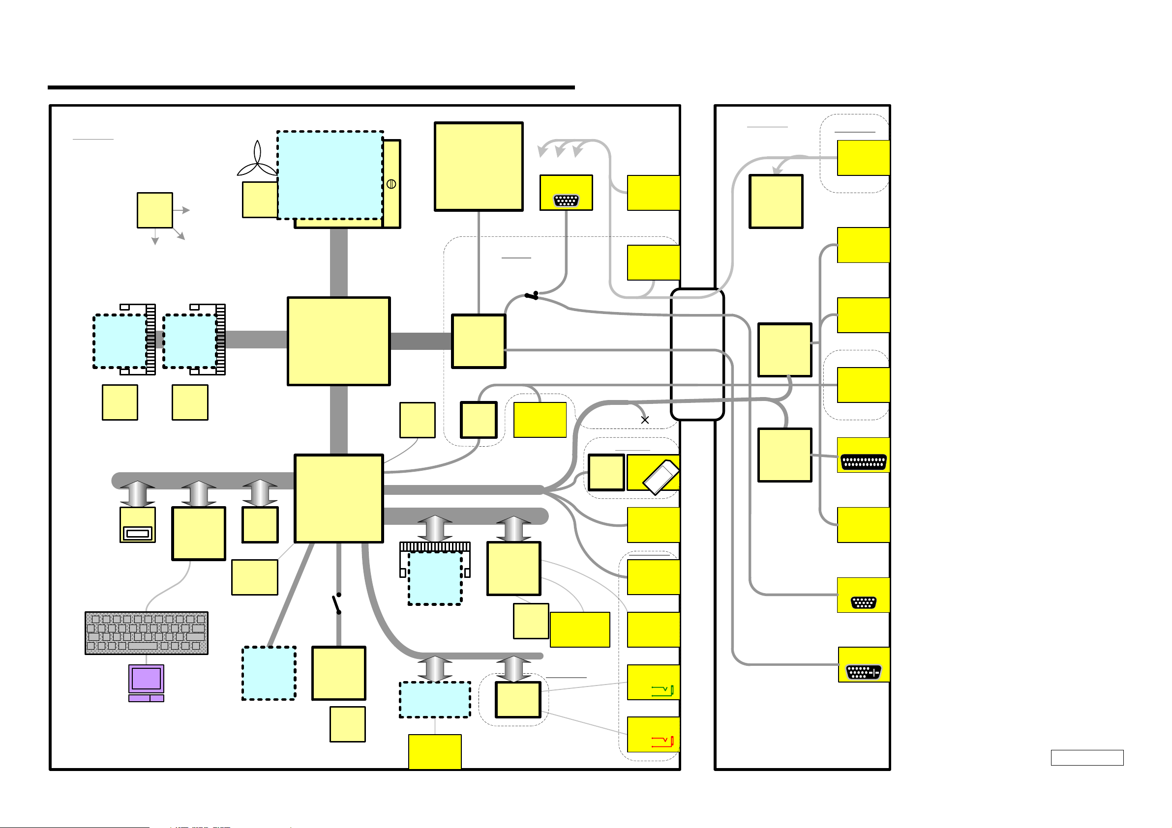
CHAPTER 1.
SPECIFICATIONS
AMJ AO
CPU PM-1.3GHz PM-1.5GHz PM-1.4GHz PM-1.4GHz PM-1.4GHz PM-1.6GHz PM-1.5GHz PM-1.5GHz PM-1.5GHz PM-1.5GHz PM-1.5GHz
LCD 12.1XGA 12.1XGA 12.1XGA 12.1XGA 12.1XGA 12.1XGA 12.1XGA 12.1XGA 12.1XGA 12.1XGA 12.1XGA
HDD 40GB 60GB 40GB 60GB 60GB 40GB 40GB 40GB 40GB 40GB 40GB
Graphics M9+X(32MB) M9+X(32MB) M9+X(32MB) M9+X(32MB) M9+X(32MB) M9+X(32MB) M9+X(32MB) M9+X(32MB) M9+X(32MB) M9+X(32MB) M9+X(32MB)
MEMORY1
QUANTITY
[STANDARD/MAX] 256MB/2GB 512MB/2GB 512MB/2GB 512MB/2GB 512MB/2GB 512MB/2GB 512MB/2GB 512MB/2GB 512MB/2GB 512MB/2GB 512MB/2GB
OPT-DRIVE CD-RW/DVD-ROM CD-RW/DVD-ROM CD-RW/DVD-ROM CD-RW/DVD-ROM CD-RW/DVD-ROM CD-RW/DVD-ROM CD-RW/DVD-ROM CD-RW/DVD-ROM Combo 9.5 Combo 9.5 Combo 9.5
internal W-LAN
AC adaptor PCGA-AC16V6 PCGA-AC16V6 PCGA-AC16V6 PCGA-AC16V6 PCGA-AC16V7 PCGA-AC16V7 PCGA-AC16V7 PCGA-AC16V7 PCGA-AC16V6 PCGA-AC16V6 PCGA-AC16V6
Battery PCGA-BP2V PCGA-BP2V PCGA-BP2V PCGA-BP2V PCGA-BP2V PCGA-BP2V PCGA-BP2V PCGA-BP2V PCGA-BP2V PCGA-BP2V PCGA-BP2V
OS WinXP Home WinXP Pro XP Home XP Home XP Pro XP Pro XP Pro XP Pro XP Pro XP Pro XP Pro
PCG-V505F/B PCG-V505W/P PCG-V505DH PCG-V505DX PCG-V505DXP PCG-V505CP PCG-V505MP PCG-V506MLP PCG-V505MSP PCG-V505MTP PCG-V505MCP
256MB × 1 512MB × 1 256MB × 2 256MB × 2 256MB × 2 512MB × 1 512MB × 1 512MB × 1 512MB × 1 512MB × 1 512MB × 1
aaaaaaaaaaa
[MA]
2
[MA]
2
[MA]
2
EU
[MA]
2
[MA]
2
[MA]
2
[MA]
3
[MA]
3
[MA]
3
• The trademarks of registered trademarks of above table, refer to page 2.
• 本表中の商標・登録商標については,2ページをご参照ください。
1-1
(END)
Confidential
PCG-V505F/V505T3x/V505W (J)
PCG-V505DC1x/V505DC1Px/V505DH/V505DX/V505DXP (AM)
PCG-V505CP (EU)
PCG-V505MCP/V505MP/V505MLP/V505MSP/V505MTP (AO)
CHAPTER 2.
BLOCK DIAGRAM
MBX-100
Clock
Gen.
SO-DIMM SO-DIMM
Thermal
Sensor
LM26
Thermal
Sensor
LM26
333 MHz
DDR
SDRAM
LPC
(33
MHz)
ATF0
LM86
Intel®
Pentium® M
Processor
478 mFCPGA
(socket)
400 MHz
PSB
Intel® 855PM
MCH
593
mFCBGA
(ODEM)
HUB
Interface
66 MHz
Intel®
82801DBM
AGP 4X
(264 MHz)
EEPROM
(MAC address)
LCD
12" XGA
LVDS
Graphics
ATI M9+
Ether
Kinnereth
USB
VIF-33
RJ-45
VGA
TMDS
Port 4
Memory
Stick
(SUMIRE 3)
Battery
DC Jack
(16 V)
Port 5
IFX-290
MS
CNX-201
DC/DC
port1
USB 2.0
Hub
port3
USB-
Parallel
CNX-206
DC Jack
(16 V)
USB
USB
RJ-45
Parallel
Debug
Internal Keyboard
TouchPad
EC/K
BC
FWH
EEPROM
(password)
HDD
421 BGA
(ICH4-M)
IDE
(Ultra ATA100)
Opt.
Drive
ATF1
LM75
PCI Bus
(33 MHz)
W-LAN
(Mini PCI
Type 3B socket)
AC'97
Bus
MDC Modem
RJ-11
i.LINK
&
PC Card
EEPROM
(GUID)
Audio
CODEC
Port 0
PC Card
(Type II x 1)
CNX-226
2-1
(END)
Port 2
USB
(right)
CNX-227
USB
(left)
i.LINK
Headphone
Microphone
USB
VGA
DVI-D
PCGA-PRV1

Confidential
PCG-V505F/V505T3x/V505W (J)
PCG-V505DC1x/V505DC1Px/V505DH/V505DX/V505DXP (AM)
PCG-V505CP (EU)
PCG-V505MCP/V505MP/V505MLP/V505MSP/V505MTP (AO)
CHAPTER 3.
FRAME HARNESS DIAGRAM
Side L
DC IN
SPEAKER
CNX-226 BOARD
SIDE A
CN5201
MONITOR
CN5130
USB
CN5120
i.LINK
MIC IN
HEADPHONE
PC CARD
L ch
1211
CN5251
PC CARD
CONNECTOR
CN5401
1
2
KEY BOARD
CN2800
(WITH HEATSINK)
12
FFC (CNX197)
CN5100
14
1
CN5101
CNX-227
BOARD
SIDE A
1
110
CN5400
124
DC FAN
CN5200
12
39 40
1211
79 80
HARNESS (WITH DC JACK 2P)
Y
A
FFC (LEX44)
M
CN2650
12
39 40
12
FPC (I.LINK&USB)
CN1401
12
LEX-52 BOARD
SIDE B
LITHIUM ION
BATTERY PACK
CN4051
18
12
910
NICKEL
HYDROGEN
BATTERY
CN60
21
CN3902
CN2660
49 50
1
CN1201
FLEXIBLE
PRINT PWB (HDD)
HDD
CN2900
12
2
114
LCD
HARNESS
(LCD)
CPU
TOUCH PAD
CN5621
29 30
12
CN5851
21
MBX-100 BOARD
SIDE A
1
12
CN2830
FFC (TP)
SWX-154
BOARD
SIDE B
RIGHT BUTTON
3-1
(END)
CN5000
CN2600
S5802
120
200181
120
200181
FFC (SWX130)
CN5801
FLEXIBLE FLAT CABLE (LEX43)
CN5300
110
CN2850
12
10
112
CENTER BUTTON
CN5800
112
S5508
LEX-51 BOARD
SIDE B
From board to connector (direct connection)
Harness (with connectors on both ends)
Harness (soldering on either end)
INVERTER UNIT
VIF-33 BOARD
SIDE A
RJ-45 HARNESS
SPEAKER
R ch
CNX-228
BOARD
(COMBO DRIVE)
CN1202
12
49 50
CN2860
1
FFC (MBX-IFX)
10
1
CN5802
S5801
LEFT BUTTON
CN2680
21
10
9
CN5700
CN2001
30 29
21
FFC (MBX-IFX)
10 1
MODEM
CARD
SWX-156
BOARD
SIDE A
110
WIRELESS
LAN CARD
DOCKING STATION
PCGA-PRV1
CN5001
2
1
HARNESS (RJ11)
IFX-290
BOARD
CN4602
SIDE A
100
99
CN4601
1
10
Side R
NETWORK
MODULAR
JACK
MEMORY
STICK
Loading...