


SLA24C164-D-3-P
Table of contents
 Loading...
Siemens SLA24C164-D-3-P, SLA24C164-D-P, SLA24C164-S-3-P, SLA24C164-S-P, SLE24C164-D-P Datasheet
...
Standard EEPROM ICs
SLx 24C164/P
16 Kbit (2048 × 8bit)
Serial CMOS-EEPROM with
2
C Synchronous 2-Wire Bus
I
and Page Protection Mode
Data Sheet 1998-07-27
™
SLx 24C164/P
Revision History: Current Version: 1998-07-27
Previous Version: 06.97
Page
(in previous
Version)
Page
(in current
Version)
Subjects (major changes since last revision)
3 3 Text was changed to “Typical programming time 5 ms for up to
16 bytes”.
55WP=
11, 12 11, 12 The erase/write cycle is finished latest after 10
V
protects the upper half entire memory.
CC
8ms.
15 15 Figure 11: second command byte is a CSR and not CSW.
21 21 The write or erase cycle is finished latest after 10
4ms.
19 24 “Capacitive l oad …” were added.
25 25 Some timings were changed.
25 25 The line “erase/write cycle” was removed.
25 25 Chapter 8.4 “Erase and Write Characteristics” has been added.
I2CBus
Purchase of Siemens I
2
C system p rovided the system conforms to the I2C specifications defined by Philips.
the I
2
C components conveys the license under the Philips I2C patent to use the components in
Edition 1998-07-27
Published by Siemens AG,
Bereich Halbleiter, MarketingKommunikation, Balanstraße 73,
81541 München
©
Siemens AG 1998.
All Rights Reserved.
Attention please!
As far as patents or other rights of third parties are concerned, liability is only assumed for components, not for applications, processes
and circuits implemented within components or assemblies.
The information describes the type of component and shall not be considered as assured characteristics.
Terms of delivery and rights to change design reserved.
For questions on technology, delivery and prices please contact the Semiconductor Group Offices in Germany or the Siemens Companies
and Representatives worldwide (see address list).
Due to technical requirements components may contain dangerous substances. For information on the types in question please contact
your nearest Siemens Office, Semiconductor Group.
Siemens AG is an approved CECC manufacturer.
Packing
Please use the recycling operators known to you. We can also help you – get in touch with your nearest sales office. B y agreement we
will take packing material back, if it is sorted. You must bear the costs of transport.
For pa cking material that is returned to us unsorted or which we are not obliged to accept, we shall have to invoice you for any costs incurred.
Components used in life-support devices or systems must be expressly authorized for such purpose!
Critical components
written appr oval of the Semiconductor Group of Siemens AG.
1 A critical component is a component used in a life-support device or system whose failure can reasonably be expected to cause the
failure of that life-support device or system, or to affect its safety or effectiveness of that device or system.
2 Life support devices or systems are intended (a) to be implanted in the human body, or (b) to support and/or maintain and sustain hu-
man life. If they fail, it is reasonable to assume that the health of the user may be endangered.
1
of the Semiconductor Group of Siemens AG, may only be used in life-support devices or systems2with the express
16 Kbit (2048 × 8bit)SerialCMOS
2
EEPROMs, I
Page Protection Mode
Features
• Data EEPROM internally organized as
2048 bytes and 128 pages × 16 bytes
• Page protection mode, flexible page-by-page
hardware write protection
– Additional protection EEPROM of 128 bits, 1 bit
per data page
– Protection setting for each data page by writing its
protection bit
– Protection managementwithoutswitching WPpin
• Low power CMOS
C Synchronous 2-Wire Bus,
™
SLx 24C164/P
P-DIP-8-4
V
•
• Two wire serial interface bus, I
= 2.7 to 5.5 V operation
CC
2
C-Bus
compatible
• Three chip select pins to address 8 devices
• Filtered inputs for noise suppression with
Schmitt trigger
P-DSO-8-3
• Clock frequency up to 400 kHz
• High programming flexibility
– Internal programming voltage
– Self timed programming cycle including erase
– Byte-write and page-write programming, between 1 and 16 bytes
– Typical programming time 5 ms for up to 16 bytes
• High reliability
6
– Endurance 10
cycles
– Data retention 40 years
1)
1)
– ESD protection 4000 V on all pins
• 8 pin DIP/DSO packages
• Available for extended temperature ranges
– Industrial: − 40 °C to + 85 °C
– Automotive: − 40°C to + 125 °C
1)
Values are temperature dependent, for further information please refer to your Siemens Sales office.
Semiconductor Group 3 1998-07-27
SLx 24C164/P
Ordering Information
Type Ordering Code Package Temperature Voltage
SLA 24C164-D/P Q67100-H3504 P-DIP-8-4 – 40 °C … + 85 °C 4.5 V...5.5 V
SLA 24C164-S/P Q67100-H3499 P-DSO-8-3 – 40 °C … + 85 °C 4.5 V...5.5 V
SLA 24C164-D-3/P Q67100-H3502 P-DIP-8-4 – 40 °C … + 85 °C 2.7 V...5.5 V
SLA 24C164-S-3/P Q67100-H3498 P-DSO-8-3 – 40 °C … + 85 °C 2.7 V...5.5 V
SLE 24C164-D/P Q67100-H3503 P-DIP-8-4 – 40°C … + 125 °C 4.5 V...5.5 V
SLE 24C164-S/P Q67100-H3497 P-DSO-8-3 – 40°C … + 125 °C 4.5 V...5.5 V
Other types are available on request
– Temperature range (– 55 °C … + 150 °C)
– Package (die, wafer delivery)
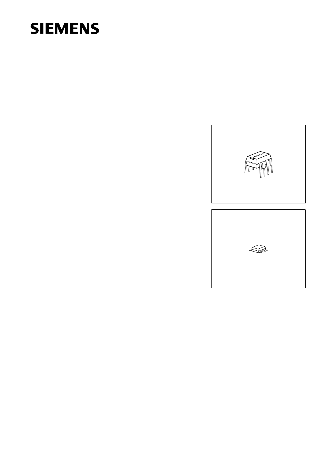
1 Pin Configuration
P-DSO-8-3
CS0
CS1
CS2
V
SS
1
2
3
4
IEP02124
CS0
CS1
CS2
V
SS
P-DIP-8-4
V
18
IEP02125
CC
72
WP
SCL63
SDA54
Figure 1
Pin Configuration (top view)
Pin Definitions and Functions
Table 1
Pin No. Symbol Function
1, 2, 3 CS0, CS1, CS2 Chip select inputs
V
8
CC
7
WP
6
SCL
SDA
5
4
V
SS
Ground
5 SDA Serial bidirectional data bus
6 SCL Serial clock input
7 WP Write protection input
8
V
CC
Semiconductor Group 4 1998-07-27
Supply voltage

SLx 24C164/P
Pin Description
Serial Clock (SCL)
The SCL input is used to clock data into the device on the rising edge and to clock data
out of the device on the falling edge.
Serial Data (SDA)
SDA is a bidirectional pin used to transfer addresses, data or control information into the
device or to transfer data out of the device. The output is open drain, performing a wired
AND function with any number of other open drain or open collector devices. The SDA
V
bus requires a pull-up resistor to
Chip Select (CS0, CS1, CS2)
CC
.
The CS0, CS1 and CS2 pins are chip select inputs either hard wired or actively driven
V
to
or VSS. These inputs allow the selection of one of eight possible devices sharing
CC
acommonbus.
Write Protection (WP)
V
WP switched to
WP switched to
allows normal read/write operations.
SS
V
protects the entire EEPROM against changes (hardware write
CC
protection).
Additionally write protection is managed by a protection bit associated to each page.
TM
(refer to chapter 7 Page Protection Mode
)
Semiconductor Group 5 1998-07-27
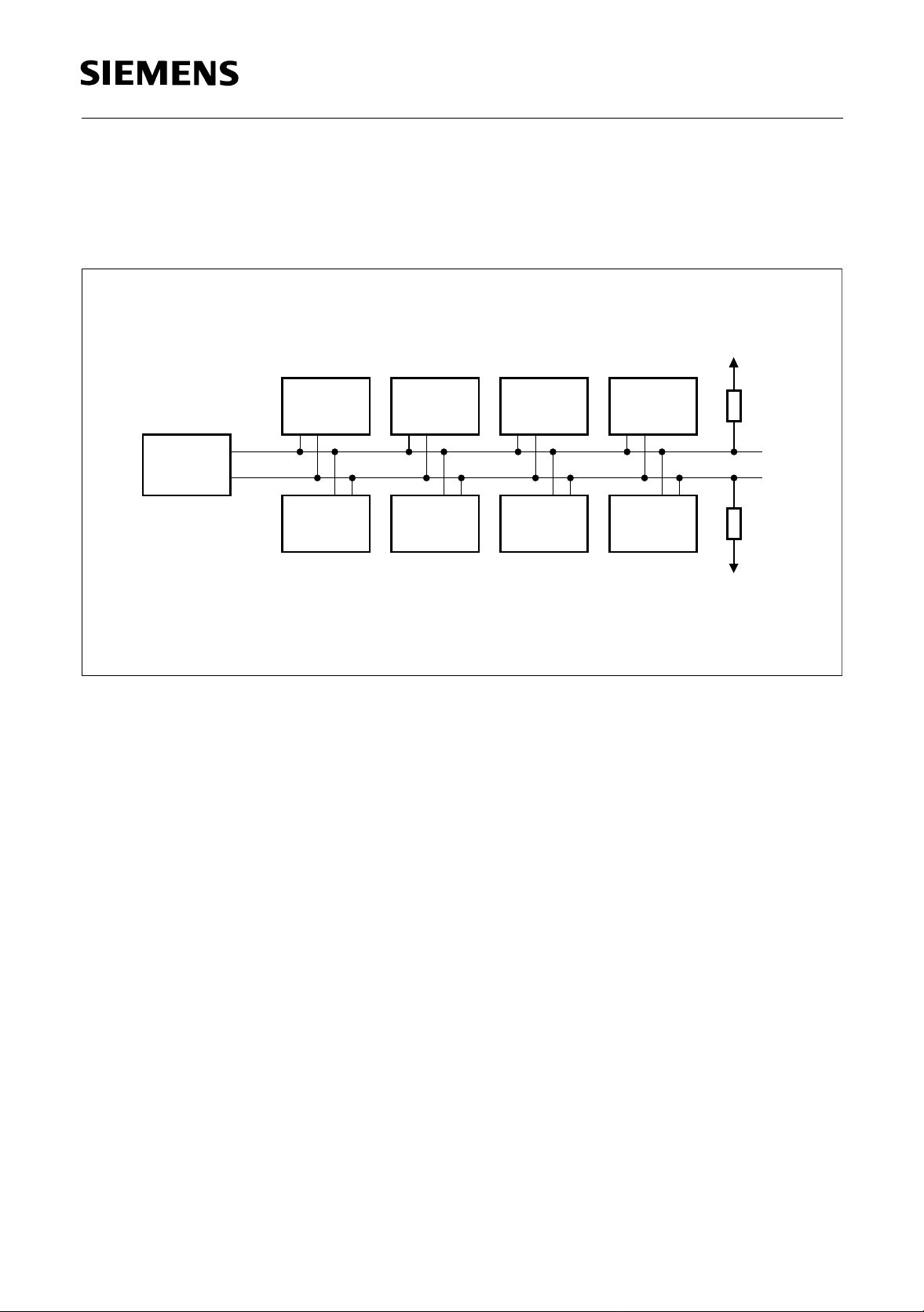
2 Description
SLx 24C164/P
The SLx 24C164/P device is a serial e
emory (EEPROM), organized as 2048 × 8 bit. The data memory is divided into
m
lectrically erasable and programmable read only
128 pages. The 16 bytes of a page can be programmed simultaneously. Each page may
be protected individually against changes by its associated protection bit.
2
The device conforms to the specification of the 2-wire serial I
2
pins allow the addressing of 8 devices on the I
C-Bus. Low voltage design permits
C-Bus. Three chip select
operation down to 2.7 V with low active and standby currents. All devices have a
6
minimum endurance of 10
erase/write cycles.
The device operates at 5.0 V ± 10% with a maximum clock frequency of 400 kHz and at
2.7 ... 4.5 V with a maximum clock frequency of 100 kHz. The device is available as 5 V
V
type (
applications and as 3 V type (
= 4.5 … 5.5 V) with two temperature ranges for industrial and automotive
CC
V
= 2.7 … 5.5 V) for industrial applications. The
CC
EEPROMs are mounted in eight-pin DIP and DSO packages or are also supplied as
chips.
V
SS
V
CC
CS0 CS1 CS2
WP
SCL
SDA
Start/
Stop
Logic
Chip Address
Control
Logic
Serial
Control
Logic
Address
Logic
Programming
Control
H.V. Pump
X
EEPROM
DEC
Page Logic
Dout/ACK
Page
Prot. Bit
EEPROM
Y DEC
IEB02271
Figure 2
Block Diagram
Semiconductor Group 6 1998-07-27
SLx 24C164/P
3 I2C-Bus Characteristics
The SLx 24C164/P devices support a master/slave bidirectional bus oriented protocol in
which the EEPROM always takes the role of a slave.
V
CC
Slave 1 Slave 2 Slave 3 Slave 4
SCL
Master
SDA
Slave 8Slave 5 Slave 6 Slave 7
V
CC
IES02183
Figure 3
Bus Configuration
Master Device that initiates the transfer of data and provides the clock for both
transmit and receive operations.
Slave Device addressed by the master, capable of receiving and transmitting
data.
Transmitter The device with the SDA as output is defined as the transmitter. Due to
the open drain characteristic of the SDA output the device applying a low
level wins.
Receiver The device with the SDA as input is defined as the receiver.
Semiconductor Group 7 1998-07-27

SLx 24C164/P
The conventions for the serial clock line and the bidirectional data line are shown in
figure 4.
SCL
SDA
START Condition Data allowed STOP Condition
12
to Change
8
Acknowledge
9
ACK ACK
1
9
IED02128
Figure 4
2
C-Bus Timing Conventions for START Condition, STOP Condition, Data Valida-
I
tion and Transfer of Acknowledge ACK
Standby Mode in which the bus is not busy (no serial transmission, no
programming): both clock (SCL) and data line (SDA) are in high
state. The device enters the standby mode after a STOP condition
or after a programming cycle.
START Condition High to low transition of SDA when SCL is high, preceding all
commands.
STOP Condition Low to high transition of SDA when SCL is high, terminating all
communications. A STOP condition initiates an EEPROM
programming cycle. A STOP condition after reading a data byte
from the EEPROM initiates the Standby mode.
Acknowledge A successful reception of eight data bits is indicated by the
receiver by pulling down the SDA line during the following clock
cycle of SCL (ACK). The transmitter on the other hand has to
release the SDA line after the transmission of eight data bits.
The EEPROM as the receiving device responds with an
acknowledge, when addressed. The master, on the other side,
acknowledges each data byte transmitted by the EEPROM and
can at any time end a read operation by releasing the SDA line (no
ACK) followed by a STOP condition.
Data Transfer Data must change only during low SCL state, data remains valid
on the SDA bus during high SCL state. Nine clock pulses are
required to transfer one data byte, the most significant bit (MSB)
is transmitted first.
Semiconductor Group 8 1998-07-27
SLx 24C164/P
4 Device Addressing and EEPROM Addressing
After a START condition, the master always transmits a Command Byte CSW or CSR.
After the acknowledge of the EEPROM a Control Byte follows, its content and the
transmitter depend on the previous Command Byte. The description of the Command
and Control Bytes is shown in table 2.
Command Byte Selects one of the 8 addressable devices: the chip select bits c2,
and c0 (bit positions b6 to b4) are compared to their
c1
corresponding hard wired input pins CS2, CS1 and CS0,
respectively (c1
Selects operation: the least significant bit b0 is low for a write
operation (C
read operation (C
Contains address information: in the CSW Command Byte, the
bit positions b3 to b1 are decoded for the three uppermost EEPROM
address bits A10, A9, A8 (in the CSR Command Byte, the bit
positions b3 to b1 are left undefined).
is the complement of CS1 pin).
hip Select Write Command Byte CSW) or set high for a
hip Select Read Command Byte CSR).
Control Byte Following CSW (b0 = 0): contains the eight lower bits of the
EEPROM address (EEA) bit A7 to A0, or an additional command
byte for the handling of the protection bit.
Following CSR (b0 = 1): contains the data read out, transmitted by
the EEPROM. The EEPROM data are read as long as the master
pulls down SDA after each byte in order to acknowledge the
transfer. The read operation is stopped by the master by releasing
SDA (no acknowledge is applied) followed by a STOP condition.
Table 2
2
Command and Control Byte for I
C-Bus Addressing of Chip and EEPROM
Definition Function
b7 b6 b5 b4 b3 b2 b1 b0
CSW 1 c2 c1
CSR 1 c2 c1
c0A10A9A80 ChipSelectforWrite
c0 x x x 1 Chip Select for Read
EEA A7 A6 A5 A4 A3 A2 A1 A0 EEPROM address
The device has an internal address counter which points to the current EEPROM
address.
The address counter is incremented
– after a data byte to be written has been acknowledged, during entry of further data
byte
– during a byte read, thus the address counter points to the following address after
reading a data byte.
Semiconductor Group 9 1998-07-27
Loading...