


CD-C401W,CP-C402
SERVICE MANUAL
No. S7751CDC401W/
CD-C401W
CP-C402
CD-C401W and CP-C402 constitute CD-C401W.
• In the interests of user-safety the set should be restored to its original condition and only parts identical to those specified be used.
CONTENTS |
|
|
Page |
SAFETY PRECAUTION FOR SERVICE MANUAL .......................................................................................................... |
2 |
VOLTAGE SELECTOR ..................................................................................................................................................... |
2 |
AC POWER SUPPLY CORD AND AC PLUG ADAPTOR ................................................................................................ |
2 |
SPECIFICATIONS ............................................................................................................................................................ |
3 |
NAMES OF PARTS .......................................................................................................................................................... |
4 |
OPERATION MANUAL ..................................................................................................................................................... |
6 |
DISASSEMBLY ................................................................................................................................................................. |
7 |
REMOVING AND REINSTALLING THE MAIN PARTS .................................................................................................... |
9 |
ADJUSTMENT ................................................................................................................................................................ |
10 |
NOTES ON SCHEMATIC DIAGRAM ............................................................................................................................. |
12 |
TYPE OF TRANSISTER ................................................................................................................................................. |
12 |
BLOCK DIAGRAM .......................................................................................................................................................... |
13 |
SCHEMATIC DIAGRAM / WIRING SIDE OF P.W.BOARD ............................................................................................. |
16 |
VOLTAGE ....................................................................................................................................................................... |
28 |
WAVEFORMS OF CD CIRCUIT ..................................................................................................................................... |
29 |
TROUBLESHOOTING (CD SECTION) .......................................................................................................................... |
30 |
FUNCTION TABLE OF IC .............................................................................................................................................. |
34 |
DISPLAY PANEL ............................................................................................................................................................ |
40 |
REPLACEMENT PARTS LIST/EXPLODED VIEW |
|
SHARP CORPORATION
– 1 –

CD-C401W,CP-C402
SAFETY PRECAUTION FOR
SERVICE MANUAL
Precaution to be taken when replacing and servicing the Laser Pickup.
The AEL (Accessible Emission Level) of Laser Power Output for this model is specified to be lower than Class I Requirements. However, the following precautions must be observed during servicing to protect your eyes against exposure to the Laser beam.
(1)When the cabinet has been removed, the power is turned on without a compact disc, and the Pickup is on a position outer than the lead-in position, the Laser will light for several seconds to detect a disc. Do not look into the Pickup Lens.
(2)The Laser Power Output of the Pickup inside the unit and replacement service parts have already been adjusted prior to shipping.
(3)No adjustment to the Laser Power should be attempted when replacing or servicing the Pickup.
(4)Under no circumstances look directly into the Pickup Lens at any time.
(5)CAUTION - Use of controls or adjustments, or performance of procedures other than those specified herein may result in hazardous radiation exposure.
Laser Diode Properties Material: GaAIAs Wavelength: 780 nm
Emission Duration: continuous Laser Output: max. 0.6 mW
CAUTION-INVISIBLE LASER RADIATION WHEN OPEN. DO NOT STARE INTO BEAM OR VIEW DIRECTLY WITH OPTICAL INSTRUMENTS.
VARNING-OSYNLIG LASERSTRALNING NAR DENNA DEL AR OPPNAD. STIRRA EJ IN I STRALEN OCH BETRAKTA EJ STRALEN MED OPTISKA INSTRUMENT.
ADVERSEL-USYNLIG LASERSTRALING VED ABNING. SE IKKE IND I
STRALEN-HELLER IKKE MED OPTISKE INSTRUMENTER.
VARO! AVATTAESSA OLET ALTTIINA NAKYMATON LASERSATEILYLLE. ALA TUIJOTA SATEESEEN ALAKA KATSO SITA OPTISEN LAITTEEN LAPI.
VARNING-OSYNLIG LASERSTRALNING NAR DENNA DEL AR OPPNAD. STIRRA EJ IN I STRALEN OCH BETRAKTA EJ STRALEN GENOM OPTISKT INSTRUMENT.
ADVERSEL-USYNLIG LASERSTRALING NAR DEKSEL APNES. STIRR IKKE INN I STRALEN ELLER SE DIREKTE MED OPTISKE INSTRUMENTER.
VOLTAGE SELECTION
The voltage selector is located on the AC voltage selector box. If adjustment is necessary, use a screwdriver in order to turn the selector in either direction the correct voltage figure is displayed in the window next to the adjisument screw.
QACCB0004AW00 |
|
|
|
|
|
|
|
|
|
|
|
|
92LCoRD577B |
|||||||
|
|
|
|
|
|
|
|
|
|
|
|
|
|
|
|
|
|
|
|
|
|
|
|
|
|
|
|
|
|
|
|
|
|
|
|
|
|
|
|
|
|
|
|
|
|
|
|
|
|
|
|
|
|
|
|
|
|
|
|
|
|
|
QACCE0007AW00 |
|
|
|
|
|
|
|
|
92LPLUG027 |
92LPLUG155A |
||||||
|
|
|
|
|
|
|
|
|
|
|
|
|
|
|
|
|
|
|
|
|
|
|
|
|
|
|
|
|
|
|
|
|
|
|
|
|
|
|
|
|
|
|
|
|
|
|
|
|
|
|
|
|
|
|
|
|
|
|
|
|
|
|
|
|
|
|
|
92LCoRDZ1652A
Figure 2 AC POWER SUPPLY CORD AND AC PLUG ADAPTOR
– 2 –
CD-C401W,CP-C402
FOR A COMPLETE DESCRIPTION OF THE OPERATION OF THIS UNIT, PLEASE REFER TO THE OPERATION MANUAL.
SPECIFICATIONS
CD-C401W
 General
Power source: |
AC 110/127/220/230-240 V, |
|
50/60 Hz |
Power consumption: |
80 W |
Dimensions: |
Width; 270 mm (10-5/8") |
|
Height; 280 mm (11-1/16") |
|
Depth; 332.5 mm (13-1/8") |
Weight: |
4.2 kg (9.2 Ibs.) |
 Amplifier section
Output power: |
PMPO; 160 W |
|
MPO; 34 W (17 W + 17 W) |
|
(10 % T.H.D.) |
|
RMS; 20 W (10 W + 10 W) |
|
(10 % T.H.D.) |
Output terminals: |
Speakers; 8 ohms |
|
Headphones; 16 - 50 ohms |
|
(recommended; 32 ohms) |
 Tuner section
Frequency range: |
FM; 88 - 108 MHz |
|
AM; 531- 1,602 kHz |
 Cassette deck section
Frequency response: |
50 - 14,000 Hz (Normal tape) |
Signal/noise ratio: |
50 dB (TAPE 1, recording/ |
|
playback) |
|
55 dB (TAPE 2, playback) |
Wow and flutter: |
0.15 % (WRMS) |
 Compact disc player section
Type: |
3-disc multi-play compact disc |
|
|
|
player |
Signal readout: |
Non-contact, 3-beam semi- |
|
|
|
conductor laser pickup |
D/A Converter: |
1-bit D/A converter |
|
Frequency response: |
20 - 20,000 Hz |
|
Dynamic range: |
90 dB (1 kHz) |
|
|
|
|
CP-C402 |
|
|
Speaker section |
|
|
Type: |
10 cm (4") full range speaker |
|
Maximum input power: 20 W |
||
Impedance: |
8 ohms |
|
Dimensions: |
Width; 170 mm (6-11/16") |
|
|
|
Height; 280 mm (11") |
|
|
Depth; 151 mm (5-15/16") |
Weight: |
1.4 kg (3.1 Ibs.)/each |
|
Specifications for this model are subject to change without prior notice.
– 3 –
CD-C401W,CP-C402
|
|
NAMES OF PARTS |
||
|
|
1 |
||
|
CD-C401W |
|||
|
Front Panel |
|
|
|
|
|
|
|
|
1. Disc Tray |
|
|
|
|
|
|
|
||
|
|
|
|
|
|
|
|
|
|
|
|
|
|
|
|
|
|
|
|
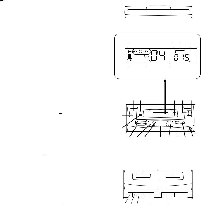
2.CD Play Indicator: 
3.Disc Number Indicators
4.FM Stereo Mode Indicator: ST
5.Extra Bass Indicator: X-BASS
6.Memory Indicator
7.CD Pause Indicator: 

8.CD Repeat Indicator: 
9.FM Stereo Indicator: 
10.Function/CD Track/CD Counter/Frequency/Preset Channel/Volume Indicator
11.On/Stand-by Switch
12.Memory Set Button
13.Clock/Timer Button
14.Extra Bass Button: X-BASS
15.Volume Up/Down Buttons: 

16.Function Selector Button
17.Band Selector Button
18.Tuning Up/Down Buttons: 

19.Track Down/Review/Preset Down Button: 


20.Play/Repeat Button: 
21.Stop Button: 
22.Track Up/Cue/Preset Up Button: 


23.Disc Skip Button
24.Open/Close Button: 
25.Headphone Socket
26.(TAPE 1) Cassette Compartment
27.(TAPE 2) Cassette Compartment
28.(TAPE 1) Record Button: 
29.(TAPE 1) Play Button: 
30.(TAPE 1) Rewind Button: 
31.(TAPE 1) Fast Forward Button: 
32.(TAPE 1) Stop/Eject Button:  /
/
33.(TAPE 2) Play Button: 
34.(TAPE 2) Stop/Eject Button:  /
/
2 |
3 |
4 |
5 |
6 |
1 |
2 |
3 |
ST X-BASS |
MEMORY |
7 |
|
|
|
|
8 |
9 |
10 |
11 12 |
|
13 14 15 |
16 |
|
|
17 |
|
|
18 19 20 |
21 |
22 23 24 25 |
26 |
27 |
|
28 29 3031 32 |
33 |
34 |
– 4 –
CD-C401W

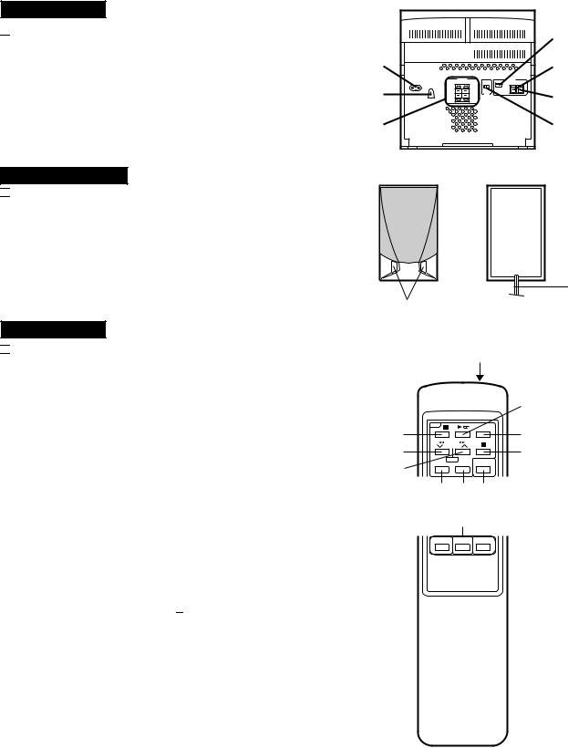
 Rear Panel
1.AC Power Input Socket
2.AC Voltage Selector
3.Speaker Terminals
4.AM Loop Aerial Input Socket
5.Aerial Earth Terminal
6.FM 75 ohms Aerial Socket
7.Span Selector Switch
CP-C402

 Speaker Section
8.Bass Reflex Duct
9.Speaker Wire
CD-C401W

 Remote Control
1. Remote Control Transmitter LED
 CD Control section
2.Stop Button: 
3.(CD) Track Down/Review Button: 

 (TUNER) Preset Down Button:
4.(CD) Track Up/Cue Button: 

 (TUNER) Preset Up Button:
5.Play/Repeat Button: 
6.Disc Skip Button
7.Pause Button: 

8.Memory Button
9.Clear Button
 Common section
10.Extra Bass Button: X-BASS
11.Function Selector Buttons
12.Power Button
13.Volume Up/Down Buttons: 

|
CD-C401W,CP-C402 |
|
4 |
1 |
5 |
2 |
6 |
3 |
7 |
9
8 |
|
|
1 |
|
5 |
2 |
6 |
3 |
7 |
4 |
|
8 |
9 10 |
|
11 |
12 
 13
13
– 5 –

– 6 –
SETTING THE CLOCK
In this example, the clock is set for the 24hour (0:00) system.
ON/STAND-BY
MEMORY/
SET

 CLOCK/
TIMER
TUNING ( )
)
1
2
3
AM 12:00 
 AM 0:00
 0:00
0:00
4
5
6
7 
8
1 Press the ON/STAND-BY switch to enter the stand-by mode.
The display brightness will decrease in stand-by mode.
2 Press the MEMORY/SET button.
3 Press the TUNING ( or ) button to select the time display |
|
mode. |
|
"AM 12:00" |
→ The 12-hour display will appear. |
|
(AM 12:00 - PM 11:59) |
"AM 0:00" |
→ The 12-hour display will appear. |
|
(AM 0:00 - PM 11:59) |
"0:00" |
→ The 24-hour display will appear. |
|
(0:00 - 23:59) |
|
Note that this can only be set when the unit is first installed |
||
4 |
or it has been reset (see below). |
||
Press the MEMORY/SET button. |
|||
5 |
Press the TUNING ( |
or |
) button to adjust the hour. |
|
Press the TUNING button once to advance the time by 1 |
||
|
hour. Press for more than 0.5 seconds to advance continu- |
||
|
ously. |
|
|
|
When the 12-hour display is selected, "AM" will change auto- |
||
6 |
matically to "PM". |
|
|
Press the MEMORY/SET button. |
|||
7 |
Press the TUNING ( |
or |
) button to adjust the minutes. |
|
Press the button for at least 0.5 seconds to advance continu- |
||
|
ously. |
|
|
|
The hour setting will not advance even if minutes advance |
||
8 |
from "59" to "00". |
|
|
Press the MEMORY/SET button. |
|||
|
The clock starts operating from "0" seconds. (Seconds are |
||
|
not displayed.) |
|
|
Note:
In the event of a power failure or when the AC power lead is disconnected, the clock display will go out.
When the AC power supply is resumed, the clock display will flash on and off to indicate that the time must be reset.
If this happens, follow steps 1 and 4 - 8 in the procedure described above.
To change the clock time:
When the ON/STAND-BY switch is set to STAND-BY.
1 Press the MEMORY/SET button.
2 Perform steps 5 - 8 above.
When the ON/STAND-BY switch is set to ON.
1 Press the CLOCK/TIMER button.
2 Within 3 seconds, press the MEMORY/SET button.
3 Perform steps 5 - 8 above.
To change the time display mode:
1 Press the ON/STAND-BY switch to enter the stand-by mode.
2 Press and hold down the  button, and then hold down the ON/STAND-BY switch for at least 1 second.
(Refer to RESETTING THE MICROCOMPUTER on page 15.)
3 Perform steps 1 - 8 above.
Note:
The operation explained above will erase all data stored in memory, such as clock and timer settings, tuner and CD presets.
PREPARATION FOR USE
0.2 m - 6 m (8" - 20')
15 |
15 |
|
Notes concerning use:
Replace the batteries if control distance decreases or operation becomes erratic.
Periodically clean the transmitter LED on the remote control and the sensor on the main unit with a soft cloth.
Exposing the sensor on the main unit to strong light may interfere with operation. Change the lighting or the direction of the unit.
Keep the remote control away from moisture, excessive heat, shock, and vibrations.
C402-C401W,CP-CD
RESETTING THE MICROCOMPUTER
1,2
2
Reset the microcomputer under the following conditions:
 To erase all of the stored memory contents (clock and timer settings, tuner and CD presets).
 If the display is not correct.
 If the operation is not correct.
1 Press the ON/STAND-BY switch to enter the stand-by mode.
2 Press and hold down the  button, and then hold down the ON/STAND-BY switch for at least 1 second.
MANUAL OPERATION
CD-C401W,CP-C402
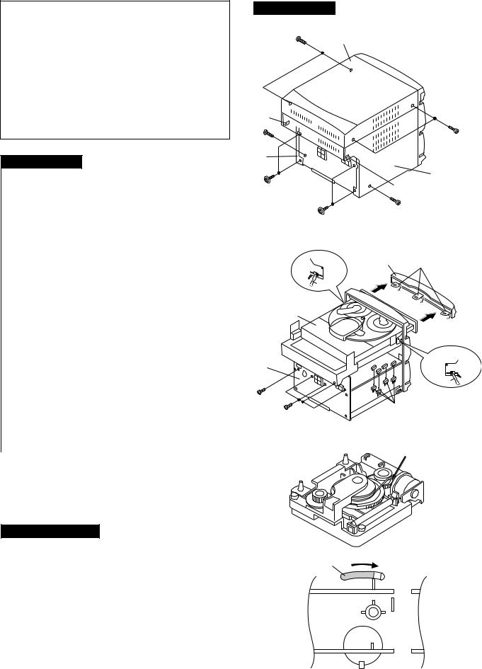
DISASSEMBLY
Caution on Disassembly
Follow the below-mentioned notes when disassembling the unit and reassembling it, to keep it safe and ensure excellent performance:
1.Take cassette tape and compact disc out of the unit.
2.Be sure to remove the power supply plug from the wall outlet before starting to disassemble the unit.
3.Take off nylon bands or wire holders where they need be removed when disassembling the unit. After servicing the unit, be sure to rearrange the leads where they were before disassembling.
4.Take sufficient care on static electricity of integrated circuits and other circuits when servicing.
CD-C401W
STEP |
REMOVAL |
|
PROCEDURE |
|
FIGURE |
|
|
|
|
|
|
1 |
Top Cabinet |
1. Screw ..................... |
(A1) x4 |
7-1 |
|
|
|
|
|
|
|
2 |
Side Panel |
1. Screw ..................... |
(B1) x6 |
7-1 |
|
|
(Left/right) |
|
|
|
|
|
|
|
|
|
|
3 |
CD Player Unit/ |
1. |
Turn on the power supply, |
7-2 |
|
|
CD Tray Cover |
|
open the disc tray, take out |
|
|
|
|
|
the CD cover, and close. |
|
|
|
|
|
(Note 1) |
|
|
|
|
2. |
Hook ....................... |
(C1) x3 |
|
|
|
3. |
Hook ....................... |
(C2) x2 |
|
|
|
4. |
Socket .................... |
(C3) x4 |
|
|
|
|
|
|
|
4 |
Back Board |
1. Screw ..................... |
(D1) x5 |
7-2 |
|
|
|
|
|
|
|
5 |
Main PWB/ |
1. Screw ..................... |
(E1) x10 |
8-1 |
|
|
Display PWB |
2. Hook ....................... |
(E2) x2 |
|
|
|
|
3. |
Socket .................... |
(E3) x5 |
|
|
|
|
|
|
|
6 |
Front Panel |
1. Screw ..................... |
(F1) x2 |
8-1 |
|
|
|
2. |
Hook ....................... |
(F2) x3 |
|
|
|
|
|
|
|
7 |
Tape Mechanism |
1. |
Open the cassette holder. |
8-2 |
|
|
|
2. |
Screw...................... |
(G1) x6 |
|
|
|
|
|
|
|
8 |
Turntable |
1. Screw ..................... |
(H1) x1 |
8-3 |
|
|
|
2. |
Cover ..................... |
(H2) x1 |
|
|
|
|
|
|
|
9 |
Disc Tray |
1. |
Screw ..................... |
(J1) x2 |
8-3 |
|
|
2. |
Guide ..................... |
(J2) x2 |
|
|
|
|
|
|
|
10 |
CD Changer |
1. Screw ..................... |
(K1) x4 |
8-4 |
|
|
Mechanism |
|
|
|
|
|
|
|
|
|
|
11 |
CD Mechanism |
1. Screw ..................... |
(L1) x1 |
8-4 |
|
|
|
|
|
|
|
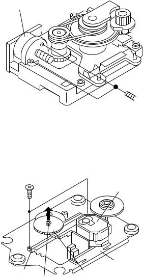
Note 1:
How to open the change manually. (Fig. 7-3)
1.Insert the tip of fine screwdriver into the hole of CD player base, and press down the worm wheel <A>.
2.Then, turn fully the lock lever in the arrow direction through the hole on the loading chassis bottom in this state.
After that, push forward the CD player base.
CP-C402
STEP |
REMOVAL |
PROCEDURE |
|
FIGURE |
|
|
|
|
|
1 |
Speaker |
1. Front panel ............. |
(A1) x1 |
8-5 |
|
|
2. Screw ...................... |
(A2) x4 |
8-6 |
|
|
|
|
|
CD-C401W
(A1)x2
ø3x12mm
Top Cabinet
Hook |
|
|
|
(B1)x1 |
|
(A1)x2 |
|
ø3x12mm |
|
||
Side Panel |
|
ø3x12mm |
|
|
|
||
(Right) |
|
|
|
|
|
Side Panel |
|
(B1)x2 |
Hook |
(Left) |
|
|
|||
ø3x12mm |
|
|
|
|
(B1)x1 |
|
|
(B1)x2 |
ø3x12mm |
||
ø3x12mm |
|
|
|
|
Figure 7-1 |
|
|
Hook |
CD Tray Cover |
Hook |
|
(C1)x3 |
|||
(C2)x1 |
|
||
|
|
||
Push |
|
|
|
Driver |
|
|
|
CD Player Unit |
|
|
|
|
|
Hook |
|
|
|
(C2)x1 |
|
Back Board |
|
Push |
|
|
|
||
|
|
Driver |
|
(D1)x1 |
|
|
|
ø3x8mm |
(C3)x4 |
|
|
(D1)x4 |
|
||
|
|
||
ø3x8mm |
|
|
|
|
Figure 7-2 |
|
|
|
< A > |
|
|
LOCK
LEVER
Figure 7-3
– 7 –

CD-C401W,CP-C402
|
Front Panel |
|
Hook |
(E1)x8 |
(E2)x2 |
ø3x10mm |
|
(E3)x2 |
|
|
Display PWB |
(E3)x1 |
Main PWB |
|
|
(E1)x2 |
|
ø3x10mm |
|
(E3)x1
(E3)x1
Hook
(F2)x3  (F1)x2
  ø3x10mm
Figure 8-1
Front Panel

 Open (G1)x6


 ø3x10mm

 Cassette
Holder (Left/Right)
Tape Mechanism
Figure 8-2
( H1 ) x1 ø3 x10mm 
( H2 ) x1
Turntable
( J1 ) x1 |
Disc Tray |
|
|
ø3 x10mm |
|
( J2 ) x1
( J1 ) x1 ø3 x10mm
CD Player Unit |
( J2 ) x1 |
|
|
Figure 8-3 |
|
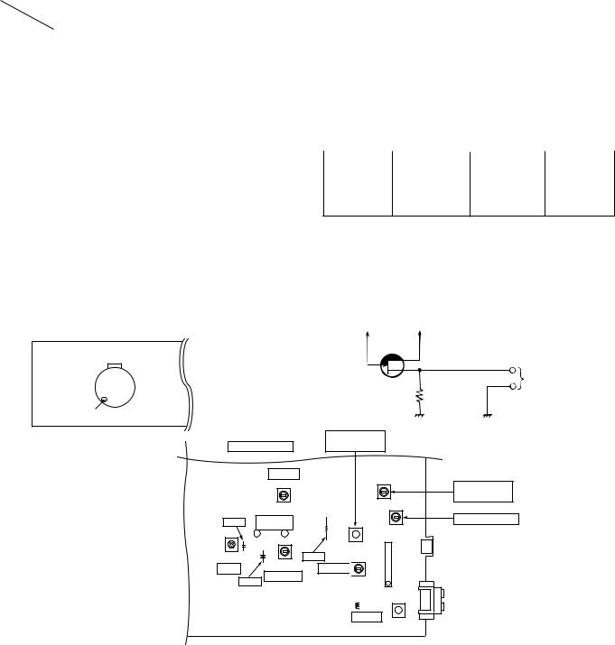
 ( K1 ) x4
 ø3 x14mm
( L1 ) x1 ø2.6 x10mm
Shift Lever
CD Changer
Mechanism
CD Player Base |
CD Mechanism |
Care when installing the CD changer mechanism.
Install the CD changer mechanism on the CD player base after the shift lever has been set in the highest position.
Figure 8-4
CP-C402
Front Panel |
Speaker Box |
|
|
(A1) x1 |
|
Driver should be pried
 away from Speaker Box.
|
Screw |
Direction of handle |
Driver |
|
Figure 8-5
Woofer |
Speaker Box |
(A2) x2 ø4x12mm
Figure 8-6
– 8 –
CD-C401W,CP-C402
REMOVING AND REINSTALLING THE MAIN PARTS
CD MECHANISM SECTION
Perform steps 1, 2, 3, 13 and 14 of the disassembly method to remove the CD mechanism.
How to remove the turntable up/down motor (See Fig. 9-1)
1.Remove the screws (A1) x 2 pcs., to remove the turntable up/down motor.
How to remove the pickup (See Fig. 9-2)
1.Remove the screws (B1) x 2 pcs., to remove the shaft (B2).
2.Remove the stop washer (B3) x 1 pc., to remove the gear (B4).
3.Remove the pickup.
Turntable Up/Down
Motor
( A1 ) x2  ø2 x5mm
Figure 9-1
( B1 ) x2
 2.6 x6mm
Pickup
CD Mechanism
( B2 ) x1 ( B4 ) x1 ( B3 ) x1
Figure 9-2
– 9 –
CD-C401W,CP-C402
ADJUSTMENT
MECHANISM SECTION
∙ Driving Force Check
Torque Meter |
Specified Value |
|
|
Play: TW-2412 |
Tape 1: Over 50 g |
|
Tape 2: Over 100 g |
|
|
∙ Torque Check
Torque Meter |
Specified Value |
|
|
|
|
|
Tape 1 |
Tape 2 |
|
|
|
Play: TW-2111 |
30 to 60 g. cm |
30 to 60 g.cm |
|
|
|
Fast forward: TW-2231 |
— |
80 to 135 g.cm |
|
|
|
Rewind: TW-2231 |
— |
80 to 135 g.cm |
|
|
|
∙ Tape Speed |
|
|
|
Test Tape |
Adjusting |
Specified |
Instrument |
|
|
Point |
Value |
Connection |
|
|
|
|
|
Normal |
MTT-111 |
Volume in |
3,000 ± |
Speaker |
speed |
|
motor |
30 Hz |
terminal |
|
|
|
|
(Load |
|
|
|
|
resistance: |
|
|
|
|
8 ohms) |
|
|
|
|
|
TUNER SECTION
fL: Low-range frequency fH: High-renge frequency
∙ AM IF/RF
Signal generator: 400 Hz, 30%, AM modulated
Test Stage |
Frequency |
Frequency |
Setting/ |
Instrument |
|
|
Display |
Adjusting |
Connection |
|
|
|
Parts |
|
IF |
450 kHz |
1,602 kHz |
T351 |
*1 |
|
|
|
|
|
Band |
— |
531 kHz |
(fL): T333 |
*2 |
Coverage |
|
|
1.1 ± 0.1 V |
|
|
|
|
|
|
Tracking |
990 kHz |
990 kHz |
(fL): T331 |
*1 |
*1. Input: Antenna (CNP301), Output: TP302
*2. Input: Antenna (CNP301), Output: TP301
∙ FM RF
Signal generator: 1 kHz, 75 kHz dev., FM modulated
Test Stage |
Frequency |
Frequency |
Serring/ |
Instrument |
|
|
Display |
Adjusting |
Connection |
|
|
|
Point |
|
|
|
|
|
|
Band |
— |
88.0 MHz |
L303(fL): |
*1 |
Coverage |
|
|
3.4 V ± 50 mV |
|
|
|
|
|
|
RF |
98.00 MHz |
98.00 MHz |
L302 |
*2 |
|
(10-30 dB) |
|
|
|
|
|
|
|
|
*1. Input: Antenna (CNP301), Output: TP301
*2. Input: Antenna (CNP301), Output: Speaker terminal
∙ Detection
Signal generator: 10.7 MHz, FM sweep generator
Test |
Frequency |
Frequency |
Adjusting |
Instrument |
||
Stage |
|
|
Display |
|
Parts |
Connection |
|
|
|
|
|
|
|
Detection |
10.7 MHz |
98.00 MHz |
|
T352 |
Input: Pin 1 of |
|
|
|
|
|
|
|
IC301 |
|
|
|
|
|
|
Output: TP302 |
|
|
|
|
|
|
|
IF |
10.7 MHz |
98.00 MHz |
|
T301(Turn |
Input: Pin 1 of |
|
|
|
|
|
|
the core of |
IC301 |
|
|
|
|
|
transformer |
Output: TP302 |
|
|
|
|
|
T352 fully |
|
|
|
|
|
|
counter- |
|
|
|
|
|
|
clookwise.) |
|
|
|
|
|
|
|
|
∙ VCO Frequency |
|
|
|
|
||
|
|
|
|
|
||
Frequency |
Frequency |
|
Adjusting |
Instrument |
||
|
|
Display |
|
Parts |
Connection |
|
|
|
|
|
|||
98.00 MHz |
98.00 MHz |
VR351* |
Pin 13, Pin 21 |
|||
(60 dB) |
|
|
|
|
|
and ground |
|
|
|
|
|
|
of IC351 |
* Adjust for 76 kHz ± 200 Hz.
Notes:
After preparing the test circuit shown in Fig 10-2, connect the Pin 13 , Pin 21 and ground of the IC351 with test circuit, and measure the Value.
At this time, apply a standard unmodulated signal input and adjust the VCO.
TAPE MECHANISM |
Pin 13 of IC351 Pin 21 of IC351 |
FET : 2SK19 or 2SK54
G  D
D
S |
TO FREQUENCY |
|
COUNTER |
|
10 kohm |
Volume in motor
MAIN PWB
|
|
|
|
AM IF |
|
|
|
|
|
T351 |
|
TP303 |
|
|
IC351 |
||
|
C364 |
13 |
C360 |
21 |
|
VR351 |
+ |
|
|||
|
|
|
T352 |
||
VCO |
|
|
|
||
|
|
FM DET. |
|||
TP302 |
|||||
|
|
||||
Figure 10-2
FM BAND
COVERAGE
|
T333 |
|
AM BAND |
|
COVERAGE fL |
R319 |
AM TRAKING fL |
T331 |
|
L303 |
CNP301 |
|
AM LOOP ANTENNA |
TP301
FM IF 

T301 |
1 |
|
|
|
|
|
IC301 |
SO301 |
|
|
|
|
|
ANTENNA |
L302 |
|
TERMINAL |
FM RF
L301
Figure 10-1 ADJUSTMENT POINTS
– 10 –
CD SECTION
Since this CD system incorporates the following automatic adjustment function, when the pickup is replaced, it is not necessary to readjust it.
Since this CD unit does not need adjustment, the combination of PWB and laser pickup unit is not restricted.
• Automatic adjustment item
1.Focus offset (Fig. 11-1)
2.Tracking offset (Fig. 11-2)
3.E/F balance (tracking error balance) (Fig. 11-3)
4.RF level AGC function (HF level: constant)
5.RF level automatic follow-up of the tracking gain
This automatic adjustment is performed each time a disc is changed.
Therefore, each disc is played back using the optimal settings.
0.1s |
|
|
0.50 V |
|
|
IC1 20 |
FE |
|
|
|
FOCUS |
|
|
OFF-SET |
|
|
ADJUST |
0.1s |
|
|
0.50 V |
|
|
IC1 7 |
TE |
TRACKING |
|
|
|
|
|
OFF-SET |
|
|
1 ADJUST |
|
|
2 |
|
|
Figure 11-1 |
10ms |
|
Enlarged |
|
View |
|
0.50 V |
|
|
|
|
|
IC1 20 |
FE |
|
10ms |
|
|
0.50 V |
|
|
IC1 7 |
TE |
TRACKING |
|
|
OFF-SET |
|
|
1 ADJUST |
|
2 |
|
|
Figure 11-2 |
|
200 ms |
TRACKING/ |
|
1V/diV |
ERROR |
|
IC 1 15 |
BARANCE |
|
TO |
1 ADJUST |
|
|
||
200 ms |
|
|
1V/diV |
|
|
IC 1 7 |
2 |
|
TE |
||
|
||
|
Figure 11-3 |
CD-C401W,CP-C402
CD TEST MODE
|
|
|
|
When the PLAY |
and POWER keys are |
|||
|
|
|
||||||
|
|
|
|
pressed at the same time in OFF MODE, the |
||||
|
|
|
|
set will enter CD TEST MODE |
||||
IL is not |
|
|
|
↓ |
|
|
|
|
performed. |
|
|
"CD TEST" of LCD will light up. |
|||||
|
|
|
|
|
↓ |
|
|
|
|
|
|
|
The pickup can be moved by using the ( ) or |
||||
|
|
|
|
( ) key. |
|
|
||
|
|
|
|
|
|
|||
|
|
|
|
|
|
|
|
|
|
|
|
|
|
→ ↓ |
Press PLAY key |
|
|
|
|
|
|
|
|
|||
|
|
|
|
|
|
|
||
|
|
|
|
LASER ON |
|
|
||
|
|
|
|
|
|
|
|
|
|
|
|
|
|
↓ |
Press PLAY key |
|
|
|
|
|
|
|
|
|
|
|
|
|
|
|
|
|
|
|
|
|
|
|
|
FOCUS SERVO ON |
|
|
||
Press PLAY key
↓
TRACKING ON THE STOP SERVO OFF PLAY Display "CD 01 0:00"
Press PLAY key
↓
TRACKING ON THE STOP SERVO OFF PLAY
↓ |
Press PLAY key |
|
STOP "CD TEST" will display
Cancel method: POWER OFF
LCD display: After the PLAY or APMS MEMORY key has been pressed, the track No. and time only will appear (valid). The other items are optional.
Note: The pickup can be slid using the  or
or  key only while in the stop mode.
ALL CLEAR AND RE-START FUNCTION
When the STOP and POWER keys are pressed to turn on the power, the entire internal memory will be cleared and the mechanism will run from address 0.
All of the tuner presets, APMS, TOC and disc numbers which were last stored in memory will be cleared, and the tuner, changer mechanism and all of the other items will be initialized.
– 11 –

CD-C401W,CP-C402
NOTES ON SCHEMATIC DIAGRAM
∙Resistor:
To differentiate the units of resistors, such symbol as K and M are used: the symbol K means 1000 ohm and the symbol M means 1000 kohm and the resistor without any symbol is ohm-type resistor. Besides, the one with “Fusible” is a fuse type.
∙Capacitor:
To indicate the unit of capacitor, a symbol P is used: this symbol P means micro-micro-farad and the unit of the capacitor without such a symbol is microfarad. As to electrolytic capacitor, the expression “capacitance/withstand voltage” is used.
(CH), (TH), (RH), (UJ): Temperature compensation (ML): Mylar type
(P.P.): Polypropylene type
∙Schematic diagram and Wiring Side of P.W.Board for this model are subject to change for improvement without prior notice.
∙The indicated voltage in each section is the one measured by Digital Multimeter between such a section and the chassis with no signal given.
1.In the tuner section, ( ) indicates AM
< > indicates FM stereo
2.In the main section, a tape is being played back.
3.In the deck section, a tape is being played back. ( ) indicates the record state.
4.In the power section, a tape is being played back.
5.In the CD section, the CD is stopped.
∙Parts marked with “ ” (
” ( 


 ) are important for maintaining the safety of the set. Be sure to replace these parts with specified ones for maintaining the safety and performance of the set.
REF. NO |
DESCRIPTION |
POSITION |
|
|
|
SW1 |
OPEN/CLOSE |
ON—OFF |
|
|
|
SW2 |
MECHA UP |
ON—OFF |
|
|
|
SW3 |
DISC NUMBER |
ON—OFF |
|
|
|
SW4 |
PICKUP IN |
ON—OFF |
|
|
|
SW605 |
TAPE 1 MAIN |
ON—OFF |
|
|
|
SW606 |
TAPE 2 MAIN |
ON—OFF |
|
|
|
SW607 |
REC. |
ON—OFF |
|
|
|
SW608 |
TAPE 1 PLAY |
ON—OFF |
|
|
|
SW701 |
POWER |
ON—OFF |
|
|
|
SW702 |
VOLUME UP |
ON—OFF |
|
|
|
SW703 |
VOLUME DOWN |
ON—OFF |
|
|
|
SW704 |
PLAY |
ON—OFF |
|
|
|
SW705 |
FF |
ON—OFF |
|
|
|
SW706 |
REW |
ON—OFF |
|
|
|
SW707 |
OPEN/CLOSE |
ON—OFF |
|
|
|
REF. NO |
DESCRIPTION |
POSITION |
|
|
|
SW708 |
STOP |
ON—OFF |
|
|
|
SW709 |
DISC SKIP |
ON—OFF |
|
|
|
SW710 |
X-BASS |
ON—OFF |
|
|
|
SW711 |
FUNCTION |
ON—OFF |
SW712 |
BAND |
ON—OFF |
|
|
|
SW713 |
CLOCK/TIMER |
ON—OFF |
|
|
|
SW714 |
MEMORY |
ON—OFF |
|
|
|
SW715 |
TUNING UP |
ON—OFF |
|
|
|
SW716 |
TUNING DOWN |
ON—OFF |
|
|
|
SW718 |
SPAN SELECTOR |
50/9—100/10 |
|
|
|
SW901 |
VOLTAGE SELECTOR |
110—127— |
|
|
220—230/240 |
|
|
|
SWM 3 |
FOOL PROOF |
ON—OFF |
|
|
|
SWM 4 |
F.A.S. |
ON—OFF |
|
|
|
SWM 5 |
CAM |
ON—OFF |
|
|
|
FRONT |
|
FRONT |
||||||||||||
|
VIEW |
|
|
VIEW |
||||||||||
|
|
|
|
|
|
|
|
|
|
|
|
|
|
|
|
|
|
|
|
|
|
|
|
|
|
|
|
|
|
E C B |
B C E |
|
(S) (G)(D) |
(D)(G)(S) |
|
(1) (2) (3) |
(3) (2) (1) |
|
2SC1845 F |
KRC104 M |
2SD2012 Y |
2SC380 O |
KTA1266 GR |
|
KRA102 M |
KTA1271 Y |
|
KRA109 M |
KTC3199 GR |
|
KRC102 M |
KTC3203 Y |
|
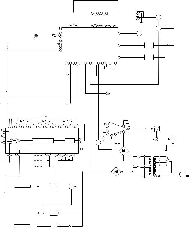
Figure 12 TYPES OF TRANSISTOR
– 12 –
13 – |
BLOCK 13 Figure |
– |
DIAGRAM |
|
(1/3) |
PICKUP UNIT
FOCUS COIL
TRACKING COIL
M2 |
M1 |
SLED |
SPINDLE |
MOTOR |
MOTOR |
M |
M |
PICKUP IN
SW4
VOLTAGE |
|
|
|
|
|
|
|
|
|
|
|
|
REGULATOR |
+5V |
|
|
|
|
|
|
|
|
|
|
|
Q1 |
|
|
|
|
|
+5V |
|
|
|
|
|
|
|
|
|
|
XL1 |
|
|
|
|
|
|
|
|
|
|
|
|
|
|
|
|
|
|
|
|
|
62 |
64 |
56 |
|
45 |
44 |
6 23 36 41 43 |
|
|
|
|
|
|
LD0 |
VCC1 |
VCC2 |
|
XIN |
XOUT |
VVDD VDD LVDD |
RVDD XVDD |
|
|
|
|
|
|
|
|
|
|
|
|
|
|||||
|
|
|
|
|
IC2 |
LCHO37 |
|
|
|
|
||
|
IC1 |
|
|
|
LVSS |
38 |
|
|
|
TO MAIN SECTION |
||
|
|
|
|
LC78623D |
RVSS |
39 |
|
|
|
|||
|
|
|
|
|
|
|
|
|||||
|
|
|
|
|
RCHO |
40 |
|
|
|
( TO IC401 ) |
||
LA9241M |
|
|
9 EFMO SERVO/SIGNAL |
|
|
|
|
|||||
JP– 32 |
|
|
|
|
|
|||||||
|
|
|
|
|
|
|
|
|
|
|
||
1 FIN2 |
|
|
~ |
10 EFMIN |
|
|
|
|
|
|
|
|
2 FIN1 SERVO AMP. CV+ |
40 |
12 CLV+ |
CONTROL |
|
|
|
|
|
|
|||
3 E |
|
SLC 43 |
~ |
|
|
|
|
|
|
|
|
|
4 F |
|
SL1 |
44 |
20 JP– |
|
|
CONT1 |
24 |
1 |
IC91 |
6 |
+B5 |
|
|
|
|
|
|
|
TA7291 |
|||||
|
|
|
|
|
|
|
|
|
|
|
|
|
TO FD SPO SP SLD |
SL– SL+ DRF |
CL DAT CE |
|
RES. CQCK. COIN |
CONT2 25 |
9 |
MOTOR |
5 |
|
|||
|
SQOUT. RWC. WRQ |
|
|
|
CONTROL |
|
|
|||||
15 16 27 23 29 |
30 31 54 |
51 52 53 |
|
|
53 ~ 58 |
26 |
|
|
|
3 7 |
|
|
|
5 22 32 |
6 |
|
7 |
IC5 |
12 |
13 |
M56748FP |
|
|
24 |
DRIVER |
25 |
|
30 |
|
31 |
|
|
8 9 10 11 |
Q93 |
SWITCHING |
CL, DAT, SELIAL CONTROL/CE |
|
|
VOLTAGE |
|
REGULATOR |
Q91 |
+12V(+B3) |
|
FROM POWER AMP. |
SL+. SL–. DRF |
SECTION |
20 +B5
+B5
26
27
28
29
34
35

36
PU-IN SW
+5V 
+B5 
10 |
GND (D) |
10 |
|
SW2 |
9 |
MECHA UP |
9 |
|
MECHA UP |
|
|
|||
8 |
GND (D) |
8 |
|
SW3 |
7 |
DISK NO. |
7 |
|
DISC NUMBER |
6 |
OPEN/CLOSE |
6 |
|
SW1 |
5 |
GND (D) |
5 |
|
OPEN/CLOSE |
4 |
M– |
4 |
M |
M3 |
3 |
M+ |
3 |
LOADING |
|
2 |
GND (M) |
2 |
|
|
1 |
|
1 |
|
SOLM1 |
CNP10 |
CNS10 |
|
|
|
TO DISPLAY
SECTION
VOLTAGE
REGULATOR
Q81 |
+5V (+B5) |
FROM POWER AMP.
SECTION
C402-C401W,CP-CD

CD-C401W,CP-C402
|
|
|
|
FM FRONT END |
|
|
|
|||
|
|
|
|
|
IC301 |
|
|
|
|
|
|
|
|
|
TA7358AP |
|
|
|
|
||
SO301 |
|
|
|
MIX |
|
B.A |
|
|
|
|
ANTENNA |
|
RF |
|
|
|
|
|
|
||
|
|
|
|
|
|
|
|
|||
TERMINAL |
|
|
|
|
|
|
|
OSC |
|
FM IF IN |
|
|
|
|
|
|
|
|
|
||
|
|
|
|
|
|
|
|
|
|
|
FM75ohms |
1 |
|
3 |
4 |
6 |
5 |
7 |
8 |
9 |
10.7MHz |
|
CF302 |
|||||||||
|
|
|
|
|
|
|
|
|
|
|
L301 |
|
FM IN |
|
VD301 |
|
|
|
|
|
|
|
|
|
|
|
|
|
|
|
|
|
AM LOOP |
|
|
|
|
|
|
|
|
|
VD302 |
|
|
L302 |
|
T301 |
|
L303 |
|
|
||
ANTENNA |
|
FM RF |
|
|
FM IF |
|
FM |
|
|
|
|
|
|
|
|
|
|
||||
|
|
|
|
|
|
|
|
OSC. |
|
|
|
|
|
|
|
|
|
|
|
|
FM +B |
2 |
|
|
|
|
|
|
|
|
|
|
1 |
|
|
|
|
|
|
|
|
|
|
CNP301 |
|
|
|
|
|
|
|
|
|
|
AM ANT. |
|
|
|
|
|
|
|
|
|
|
TERMINAL |
|
|
|
|
|
|
|
|
|
|
|
|
T331 |
AM ANT. |
T333 |
AM OSC. |
|
|
|
|
|
|
|
|
|
|
|
|
|
|
|
RF AMP |
|
|
VD331-1 |
|
VD331-2 |
|
|
|
Q302 |
||
|
|
|
|
|
|
|
||||
|
|
|
|
|
|
|
|
|
D381 |
|
|
CD |
|
|
|
|
|
|
|
|
|
SECTION |
|
|
|
|
|
|
|
M601 |
M |
|
|
|
|
|
|
|
|
MOTORTAPE |
|
|
|
|
|
|
|
|
|
|
|
|
|
D201 |
D202 |
|
|
|
|
|
|
|
|
|
|
|
+B4 |
|
|
|
|
SW606 |
|
|
|
|
|
|
|
|
|
T2 MAIN |
|
|
|
|
|
|
|
|
|
SW605 |
|
|
|
|
|
|
|
|
|
T1 MAIN |
|
|
|
|
|
|
|
|
|
SW608 |
|
|
|
|
|
|
|
|
|
T1 PLAY |
|
|
|
|
|
|
|
|
|
|
|
REC. /P. B. AMP. |
|
|
|
||
TAPE1 |
|
|
|
|
IC201 |
|
|
|
|
|
|
|
|
AN7345K |
|
|
VCC |
|
|
P.B. HEAD |
|
|
|
|
|
|
|
|
|
L-CH |
REC |
PB |
T1 L |
1 |
|
|
13 |
+B5 |
|
R-CH |
|
P. B |
|
|
|
|
|||
|
SWITCHING |
T1 R |
24 |
L |
4 L OUT |
|
|||
TAPE2 |
|
|
|||||||
|
Q201 |
T2 L |
2 |
|
R |
21 R OUT |
|
||
REC/P. B. HEAD |
|
~ |
23 |
|
|
|
|
|
|
L-CH |
|
Q206 |
T2 R |
|
|
|
|
|
|
|
|
|
|
|
|
|
|||
R-CH |
|
|
L NF |
3 |
|
|
|
T1/T2 |
|
|
|
|
|
|
19 |
|
|||
|
|
|
R NF 22 |
|
|
|
|
||
|
|
|
|
|
|
|
|
||
|
|
|
POP |
|
|
|
7 L REC IN |
|
|
|
|
|
REDUCE 6 |
|
|
|
|||
|
|
|
L REC |
9 |
REC |
|
18 |
R REC IN |
|
|
|
|
|
16 |
|
|
8 |
|
|
|
|
|
R REC |
|
|
Q210 |
REC MUTING |
||
|
|
|
|
|
|
17 |
|||
|
|
|
|
|
|
|
Q213 |
||
|
|
|
|
12 |
|
|
|
|
|
|
|
|
|
|
|
|
|
|
|
|
|
|
|
|
ALC |
|
|
|
|
|
|
|
|
|
10 |
11 |
|
|
|
|
|
|
|
|
|
|
ALC CUT |
|
|
|
|
|
SWITCHING |
|
|
|
|
||
|
|
|
Q207~ |
|
|
|
|
|
|
|
|
|
Q209 |
|
|
|
|
|
|
ERASE |
Q212 |
|
L203 |
||
HEAD |
||
|
||
|
BIAS OSC |
|
|
|
|
|
|
|
|
|
|
|
|
+B5 |
|
|
AM IF |
|
|
FM DET |
SWITCHING |
||||||
|
|
|
|
|
|
|||||||
|
T351 |
CF351 |
|
T352 |
|
|
|
FM/AM |
Q352 |
FM +B |
||
|
|
OUT |
IN |
|
|
|
|
VCC |
||||
|
|
|
|
|
|
|
|
|||||
|
|
AM MIX |
AM IF |
|
|
|
|
|
|
|||
1 |
3 |
|
|
5 |
|
20 |
|
|
21 |
11 |
|
|
|
|
|
IC351 |
|
FM DET |
|
|
|
L |
|
||
|
|
|
|
|
|
|
|
|
|
|||
|
|
|
LA1805 |
|
|
|
|
L OUT 9 |
|
|||
|
|
|
|
|
|
|
R OUT 10 R |
|
||||
FM IF DET. /FM MPX. /AM IF |
|
|
||||||||||
8 6 |
22 |
23 24 |
17 |
|
16 |
7 |
15 |
13 |
|
|
||
|
INRFAM |
+BAM |
OSCAM |
OUTDET |
|
INMPX |
STEREO |
MONO/ST |
|
|
VR351 |
|
|
|
|
|
|
|
|
|
|
|
|
FM VCO |
|
|
|
|
|
Q351 |
|
|
|
|
|
|
||
|
|
|
|
|
|
|
|
|
|
|
|
D382 |
|
|
|
|
MUTING |
|
|
|
|
|
|
||
|
|
|
X381 |
|
|
|
|
|
|
|
|
|
|
|
|
4.5MHz |
|
|
|
|
|
|
|
|
|
|
VT |
|
1 |
FM IN |
AM IN |
ST |
ST |
|
|
|
|
|
|
20 |
22 |
16 15 |
11 |
10 |
10 |
|
VOLTAGE |
||||
|
|
|
|
IC381 |
|
|
|
|
|
REGULATOR |
||
|
|
|
|
|
|
|
VDD 17 |
ZD381 |
||||
|
|
|
|
LC72131 |
|
|
|
|||||
|
|
|
|
PLL |
|
|
|
|
|
|
||
|
7 |
|
|
|
|
3 |
4 |
5 |
6 |
21 |
|
|
|
FM |
|
|
|
|
CE |
DI |
CL |
DO |
|
|
|
|
Q381 |
|
+B5 |
|
|
|
|
|
|
|
|
|
SWITCHING |
|
|
|
|
|
|
|
|
|
|||
|
|
CE DI |
CL |
9 4 |
|
L |
25 24 23 |
||
|
21 |
|
|
|
|
CD |
|
|
|
|
|
|
|
|
|
R |
28 |
|
|
|
L |
19 |
|
|
T2 ON |
TUNER |
|
|
|
|
|
|
||
R |
30 |
|
|
|
|
|
|
||
|
L |
17 |
|
|
|
TAPE |
|
|
|
|
|
|
|
|
|
R |
32 |
|
|
T1 PLAY |
|
|
|
|
|
|
16 |
33 |
14 |
|
|
L |
R |
L |
T1/T2 |
|
|
|
|
TO
REC |
+B4 |
Q211 |
|
SWITCHING |
|
REC |
|
SW607 |
TO |
Figure 14 BLOCK DIAGRAM (2/3)
– 14 –
CD-C401W,CP-C402
|
LCD701 |
|
|
|
|
|
|
|
|
COM 0 ~ |
|
|
|
|
|
|
|
|
COM 3 |
S0 ~ S20 |
LMP1 |
|
|
|||
|
25 |
~ 22 |
21 |
~ |
1 |
SWITCHING |
|
|
|
|
|
||||||
|
|
|
|
|
|
LMP2 |
Q704 |
|
|
|
|
|
|
|
|
|
|
LCD BIAS |
|
|
|
|
|
|
|
|
25 ~ 28 |
21 |
~ 24 |
1 |
~ |
9 69 |
~ 80 |
Q705 |
+B5 |
29 |
COM OUT |
|
SEG OUT |
|
||||
|
|
RESET |
|
|||||
KEY MATRIX |
~ |
32 |
RESET 68 |
SWITCHING |
Q701 |
SW702 ~ SW716 |
34 |
|
|
~ |
KEY IN |
|
|
|
|
|
|
|
37 |
|
|
IC701 |
|
|
|
|
DO |
|
|
|
|
|
|
|
|
63 |
|
|
IX0182AW |
|
|
Q702 |
D703 |
|
DI |
|
|
SYSTEM STOP 13 |
+B6 |
||||
65 |
|
|
SYSTEM |
Q703 |
||||
CE |
|
|
|
|
|
|||
CL |
66 |
|
|
MICROCOMPUTOR |
|
POWER FAIL |
|
|
64 |
|
|
|
|
||||
|
|
|
|
|
|
DETECTOR |
|
|
|
|
INITIAL1 |
|
|
|
|
|
|
|
|
INITIAL2 |
|
|
|
REMOCON 38 |
RX701 |
|
|
|
|
|
|
|
|
||
|
|
|
|
40 ~ 51 60 52 |
|
|
REMOCON |
|
|
|
61 62 67 |
53 53 53 |
59 58 |
|
|
||
|
|
T1 PLAY T2 ON |
T1/T2 |
POWERCONT. |
POWERCONT. |
XL701 |
|
|
|
|
|
|
|
VDD |
|
|
|
|
|
|
|
|
|
4.19MHz |
|
|
|
|
|
|
|
|
SW718 |
|
|
|
|
|
|
|
|
SPAN |
|
|
|
|
|
|
|
|
SELECTOR |
|
|
|
|
|
|
|
|
|
GRAPHIC EQUALIZER |
|
|
|
|
|
|
|
|
|
|
|
|
|
|
|
|||
|
|
|
|
|
|
|
|
|
|
|
|
|
|
|
|
|
|
IC601 |
|
|
|
|
|
|
|
|
|
|
|
|
|
|
|
|
|
|
|
|
|
|
|
|
|
LA4282 |
|
|
|
|
|
|
|
|
|
|
|
|
|
|
|
|
|
|
|
|
|
|
|
|
|
POWER AMP. |
|
|
|
|
|||
|
CE |
DI |
CL |
9 40 |
8 41 |
7 42 |
6 43 |
|
4 45 |
|
2 47 |
1 48 |
|
|
|
2 L-IN |
|
|
9 |
L-OUT |
|
|
|
||
|
25 24 23 |
5 44 |
3 46 |
|
|
|
5 R-IN |
|
|
J601 |
|
|
|||||||||||||
L |
|
|
|
|
|
|
11 |
|
|
||||||||||||||||
21 |
|
|
|
|
IC431 |
|
|
|
|
|
|
|
|
|
|
|
|
|
7 R-OUT |
HEADPHONES |
|
||||
R |
|
|
|
|
|
|
|
|
|
|
|
|
1 |
NF |
|
|
10 |
|
|
|
|||||
28 |
|
|
|
|
|
|
|
|
|
|
|
|
|
12 |
|
|
|
|
|||||||
|
|
|
|
|
|
LC75394E |
|
|
|
|
|
|
|
|
6 |
|
4 |
|
|
|
|
|
|||
L |
|
|
|
|
|
|
|
|
|
|
|
|
|
3 |
|
|
|
|
|
|
|||||
19 |
|
|
|
AUDIO PROCESSOR |
|
|
|
|
|
|
|
|
GND |
VCC33V |
|
|
|
|
|||||||
|
|
|
|
|
|
|
|
|
OUT |
|
|
GND |
|
|
|
|
|||||||||
R |
30 |
|
|
|
|
|
|
|
|
|
|
|
|
|
|
|
CONT |
|
|
|
|
||||
|
|
|
|
|
|
|
|
|
|
VOLUME |
58 |
L |
|
|
|
|
|
|
|
|
|
|
|||
L |
|
|
|
|
|
GRAPHIC EQUALIZER |
|
|
|
|
|
|
|
|
|
|
|
|
|||||||
17 |
|
|
|
|
|
|
55 R |
|
|
|
|
|
|
|
SPEAKER SWITCH |
|
|
||||||||
|
|
|
|
|
|
|
|
|
|
|
|
|
|
Q641 |
|
|
|
|
|
|
|
||||
R |
32 |
|
|
|
|
|
|
|
|
|
|
|
|
|
|
|
VOLTAGE |
P- |
|
|
|
|
|
|
|
|
|
|
|
|
|
|
VREFL |
VREFR |
|
|
|
|
|
|
|
|
|
|
|
|
D901 ~ D904 |
|
|
|
|
|
|
|
|
|
|
REFV |
VSS VSSA |
|
|
|
|
|
|
|
REGULATOR |
|
|
|
|
POWER |
TERMINAL |
|
|||
|
|
|
|
|
|
|
|
|
|
|
|
|
VDD |
57 |
|
+B5 |
|
|
|
|
|
|
SO601 |
|
|
|
|
|
|
|
|
|
|
|
|
|
|
|
|
|
|
|
|
|
|
T901 |
SPEAKER |
|
|||
|
|
|
|
|
|
|
|
|
|
|
|
|
|
|
|
|
|
|
|
|
|
|
|
||
|
|
16 33 |
14 35 |
|
56 |
63 |
50 |
26 27 |
12 37 |
11 38 |
10 39 |
|
|
|
|
|
|
|
|
F901 |
TRANSFORMER |
|
|
||
|
|
R |
|
|
|
|
|
|
|
|
T2.5A L 250V |
230-240V |
SW901 |
|
|||||||||||
|
L |
R |
L |
|
|
|
|
|
|
|
|
|
|
|
|
|
|
|
|
|
|
||||
|
|
|
|
|
|
|
|
|
|
|
|
|
|
|
|
|
|
|
|
|
|
|
|
VOLTAGE |
|
|
|
|
|
|
|
|
|
|
|
|
|
|
|
|
|
|
|
|
|
|
|
|
220V |
SELECTOR |
|
|
|
|
|
|
|
|
|
|
|
|
X- BASS |
|
|
|
|
|
|
|
|
|
|
127V |
|
|
|
|
|
|
|
|
|
|
|
|
|
|
|
|
|
|
|
|
|
|
|
|
110V |
|
|
||
|
|
|
|
|
|
|
|
|
|
|
|
|
|
|
|
|
|
D905 ~ D908 |
|
|
|
|
|||
|
|
|
|
|
|
|
|
|
|
|
|
|
|
|
|
|
|
|
|
|
|
|
|||
|
|
|
|
|
|
|
|
|
|
|
|
|
|
|
|
|
|
|
|
|
|
F902 |
|
AC SOCKET |
AC POWER |
|
|
|
|
|
|
|
|
|
|
|
|
|
|
|
|
|
|
|
|
|
|
|
SUPPLY CORD |
||
|
|
|
|
|
|
|
|
|
|
|
|
|
|
|
|
|
|
|
|
|
|
T1.6A L 250V |
|
SO901 |
|
|
|
|
|
|
|
|
|
|
|
|
|
|
|
|
|
|
|
|
|
|
|
|
T.F |
|
|
|
|
|
|
|
|
|
|
|
|
|
|
|
|
|
|
|
|
|
|
|
|
|
|
|
AC 110V/127V/220V/ |
|
|
|
|
|
|
|
|
|
|
|
|
VOLTAGE |
|
|
|
|
|
|
|
|
|
|
|
230-240V |
|
|
|
|
|
|
|
|
|
|
|
|
|
|
|
|
|
|
|
|
|
|
|
|
50/60Hz |
||
|
|
|
|
|
|
|
|
|
|
|
|
REGULATOR |
|
|
|
|
|
|
|
|
|
|
|
||
|
|
|
|
|
|
|
|
|
|
|
|
|
|
|
|
|
|
|
|
|
|
|
|
||
|
|
|
|
TO CD SECTION |
+B4 |
|
|
|
Q925 |
|
Q924 |
|
|
|
|
|
|
|
|
|
|
|
|
||
|
|
|
|
|
|
+12V |
(MECHA) |
Q926 |
|
|
|
|
|
|
|
|
|
|
|
|
|
||||
|
|
|
|
|
|
|
|
|
|
|
|
|
|
|
|
|
|
|
|
|
|||||
|
|
|
|
|
|
|
|
|
VOLTAGE |
|
|
|
|
|
|
|
|
|
|
|
|
|
|
|
|
|
|
|
|
|
|
|
|
|
REGULATOR |
|
|
|
|
|
|
|
|
|
|
|
|
|
|
||
|
|
|
|
|
|
|
|
|
VOLTAGE |
|
|
|
|
|
|
|
|
|
|
|
|
|
|
|
|
|
|
|
|
|
|
|
|
|
REGULATOR |
|
|
|
|
|
|
|
|
|
|
|
|
|
|
||
|
|
|
|
|
|
+B5 |
|
(ANALOG) |
IC922 |
|
|
|
|
|
|
|
|
|
|
|
|
|
|
|
|
|
|
|
|
|
|
+12V |
|
|
|
|
|
|
|
|
|
|
|
|
|
|
|
|
|
||
|
|
|
|
|
|
|
|
|
VOLTAGE |
|
|
|
|
|
|
|
|
|
|
|
|
|
|
|
|
|
|
|
|
|
|
|
|
|
REGULATOR |
|
|
|
|
|
|
|
|
|
|
|
|
|
|
||
|
|
|
|
TO CD SECTION |
+B6(5V) |
|
|
|
IC921 |
|
|
|
|
|
|
|
|
|
|
|
|
|
|
|
|
|
|
|
|
|
|
|
|
|
|
|
|
F921 |
|
|
|
|
|
|
|
|
|
|
|
|
|
|
|
|
|
|
|
|
|
|
|
|
|
T500mA L 250V |
|
|
|
|
|
|
|
|
|
|
|
|
|
Figure 15 BLOCK DIAGRAM (3/3)
– 15 –

CD-C401W,CP-C402
A
|
|
CNS1B |
CNS1A |
CNP1 |
B |
K |
1 |
1 |
1 |
E |
2 |
2 |
2 |
|
|
A |
3 |
3 |
3 |
|
B |
4 |
4 |
4 |
|
F |
5 |
5 |
5 |
C |
|
|
|
|
|
|
|
PICK UP UNIT |
|||
|
1 |
K |
VR1A |
|
1/16 |
|
E |
|
|||
|
2 |
A |
|
|
|
|
3 |
|
|
|
|
|
B |
|
|
|
|
|
4 |
|
|
|
|
D |
1M |
2200P |
1M |
2200P |
|
5 |
F |
|
|
|
|
|
|
|
|
||
|
1 |
|
|
|
TR+ |
|
2 |
|
|
|
|
|
|
|
|
|
|
|
3 |
|
|
|
FO+ |
|
4 |
|
|
|
|
|
5 |
|
|
|
|
6 |
FO- |
|
TR- |
||
7 |
||
|
||
8 |
ACTUATOR |
E |
|
|
|
|
CNS2B |
CNS2A |
CNP2 |
TR_ |
1 |
1 |
1 |
TR+ |
2 |
2 |
2 |
FO+ |
3 |
3 |
3 |
FO_ |
4 |
4 |
4 |
GND |
5 |
5 |
5 |
PD |
6 |
6 |
6 |
VR |
7 |
7 |
7 |
LD |
8 |
8 |
8 |
F |
|
|
|
|
CD MOTOR |
|
|
|
|
|
|
PWB-B |
CNS3B |
CNS3A |
|
|
|
|
M1 |
M |
CNP3 |
SP+ |
||
|
|
|
|
|||
|
SPINDLE |
6 |
6 |
6 |
||
|
MOTOR |
|
5 |
5 |
5 |
SP_ |
G |
|
|
SL+ |
|||
M2 |
M |
4 |
4 |
4 |
||
|
SLED |
3 |
3 |
3 |
SL_ |
|
|
MOTOR |
|
PU-IN |
|||
|
SW4 |
|
2 |
2 |
2 |
|
|
|
|
||||
|
PU-IN |
|
1 |
1 |
1 |
|
|
|
|
|
|||
H
R1
1K
C1 |
C2 |
|
|
|
|
|
|
|
|
|
|
|
|
|
|
|
|
|
|
|
|
|
|
|
|
|
|
|
|
|
|
|
|
|
|
|
|
0.01 |
47/10 |
Q1 |
R43 |
|
|
|
C40 0.33/50 |
|
|
|
|
|
|
|
|
|
|
|
|
|
|
|
|
|
|
|
|
|
|
|
|
|
R45 |
1K |
|||
|
KTA1266 GR |
|
|
|
|
C39 |
0.47/50 |
|
|
C38 .010 |
C37 |
220/6.3 |
C35 0.1/50 |
|
|
|
|
|
|
|
|
|
|
|
|
|
|
||||||||||
|
|
|
|
|
12 |
|
|
|
|
|
|
|
|
|
|
|
|
|
|
|
|
|
|
|
|
R46 |
1K |
||||||||||
|
|
|
|
|
|
|
|
|
|
|
|
|
|
|
|
|
|
|
|
|
|
|
|
|
|
|
|
|
|
|
|
|
|
||||
|
1.3V |
|
|
3.6V |
|
|
|
|
|
|
|
|
|
|
|
|
|
|
|
|
|
|
|
|
|
|
|
|
|
|
|
|
|
|
|
||
|
|
|
C24 |
|
|
|
|
|
|
|
|
|
|
|
|
|
|
|
|
|
|
|
|
|
|
|
|
|
|
|
|
|
R47 |
1K |
|||
|
C25 |
|
|
|
|
|
|
|
|
|
|
|
|
|
|
|
|
|
|
|
|
|
|
|
|
|
|
|
|
|
|
|
|
||||
|
|
3V |
1/50 |
|
|
|
|
|
|
|
|
|
|
|
|
|
|
|
|
|
|
|
|
|
|
|
|
|
|
|
|
|
|
|
|||
|
0.01 |
|
|
|
|
|
|
|
|
|
|
|
|
|
|
|
|
|
|
|
|
|
|
|
|
|
|
|
|
|
|
|
|
||||
|
|
|
|
|
|
|
|
|
|
|
|
|
|
|
|
|
|
|
|
|
|
|
|
|
|
|
|
|
|
|
|
|
|
|
|||
|
|
|
|
IC1 |
|
|
|
|
R42 560 |
|
|
|
|
|
|
|
|
|
|
|
|
|
|
|
|
|
|
|
|
|
|
|
|
|
|
||
|
LA9241M |
|
64 |
63 |
|
62 |
61 |
60 |
|
|
|
59 |
58 |
|
57 |
VCC256 |
55 |
|
54 |
53 |
52 DAT |
51 |
49 |
|
|
|
R41 4.7K C45 4.7/25 |
|
|
|
|||||||
|
SERVO AMP. |
|
VCC1 |
+ |
|
LDO |
BHI |
PHI |
|
|
|
LF2 |
VR |
|
REF1 |
FSS |
|
DRF |
CE |
CL |
CLK50 |
DEF |
|
|
|
C50 |
|
||||||||||
|
|
LDS |
|
|
|
|
|
|
|
|
|
|
|
|
|
|
|
|
|
|
|
|
|
|
|
|
|
|
|
||||||||
|
|
|
|
|
|
|
|
– |
|
|
|
|
|
|
|
|
|
|
|
|
|
|
|
|
|
|
|
|
|
|
48 |
|
|
|
|
|
|
|
|
|
|
|
|
1 |
FIN2 |
|
|
RF |
|
|
|
|
|
|
|
|
+ |
|
|
|
|
|
|
|
|
|
|
|
|
|
|
|
0.1 |
|
|
|
|
|
|
|
|
REF |
– |
|
|
|
|
|
|
|
|
|
|
– |
|
|
|
|
|
|
|
|
|
|
|
|
|
|
|
|
|||
|
|
|
|
|
|
|
|
|
|
|
|
|
|
|
|
|
|
|
|
|
|
|
|
|
|
|
|
|
|
|
|
|
(ML) |
|
|||
|
|
|
|
|
|
2 FIN1 |
+ |
|
|
|
|
|
|
|
REF |
|
|
|
|
|
|
|
|
|
|
|
|
|
TBC |
47 |
|
|
|
|
|||
|
|
|
|
|
|
– |
|
|
|
|
|
|
|
|
+ |
|
|
|
|
|
|
|
|
|
|
|
|
|
|
|
|
|
|||||
|
|
|
|
|
|
|
– |
|
FE1 |
|
|
|
|
|
DEF |
|
|
|
|
|
|
|
|
|
|
|
|
|
|
|
|
|
|||||
|
|
|
|
|
|
|
REF |
+ |
|
|
|
|
|
|
|
– |
|
EFBAL |
|
|
|
|
|
|
|
|
|
|
|
|
|
|
|
||||
|
|
|
|
|
|
3 |
E |
|
+ |
|
REF |
|
|
|
|
|
– |
|
|
FOSTA |
|
|
|
|
|
FSC |
|
|
46 |
|
|
|
|
|
|
||
|
|
|
|
|
|
F |
|
|
|
|
VCR |
|
|
|
|
|
+ |
|
HFL |
TOSTA |
|
|
|
|
CE |
|
DGND |
45 |
|
|
|
|
|
|
|||
|
C3 |
|
|
|
|
4 |
|
REF |
|
|
VCR |
|
|
|
|
|
|
|
|
|
|
|
|
|
|
SLI |
44 |
|
|
|
|
|
|
||||
|
|
|
|
|
|
|
– |
|
|
|
|
|
+ |
|
|
|
|
|
|
|
|
|
REF |
+ – |
|
|
|
C34 |
R38 |
|
|||||||
|
0.1/50 |
|
|
R3 5 |
TB |
|
|
+ |
|
|
|
|
|
VCR |
|
– |
|
DRF |
2FREQ |
|
|
|
LATOH |
CL |
|
|
C33 0.001 |
|
|
|
|||||||
|
C4 |
100K |
|
TE |
|
|
+ |
|
|
+ |
|
|
|
|
|
|
|
|
|
|
|
|
|
|
|
|
|
R36 |
R37 |
|
|||||||
|
|
|
|
|
|
|
|
|
VCR |
|
– |
|
|
|
|
|
|
|
LASER |
|
|
|
|
|
|
|
|
|
|
|
|
0.033 33K |
|
||||
|
|
|
R2 |
|
15K 6 TE- |
REF |
|
– |
|
|
|
|
|
|
|
|
|
|
|
|
|
|
|
|
|
|
|
|
|
|
|
|
(ML) |
|
|||
|
0.001 |
|
|
|
|
|
|
|
|
|
|
|
|
|
FSTA |
|
|
|
|
|
|
|
|
|
|
|
|
47K |
47K |
|
|||||||
|
|
|
C5 |
|
7 |
|
|
|
|
|
|
|
|
|
|
|
|
|
|
8/12CM |
|
|
|
|
|
|
SLC |
43 |
|
|
|
|
|||||
|
|
|
|
|
|
REF + |
|
|
|
|
+ |
|
|
|
|
|
|
|
SLOF |
|
|
|
|
|
|
|
|
|
|
|
|
|
|
||||
|
|
|
0.033(ML) |
|
|
– |
|
|
|
|
|
|
|
|
|
|
|
|
|
|
|
|
|
|
|
|
|
|
R33 |
C32 |
R34 |
|
|||||
|
R4 |
|
|
TESI |
|
|
|
REF |
|
– |
|
|
|
|
|
+ |
|
|
|
|
|
|
|
|
|
RFS– |
|
|
|
|
|||||||
|
|
|
|
|
|
|
|
|
|
|
|
|
|
|
|
|
|
|
|
|
|
|
|
|
|
|
|
|
5.6K |
27P |
1K |
|
|||||
|
|
|
|
|
|
|
|
|
|
|
|
|
|
|
|
|
|
|
VCC |
|
|
|
|
|
|
|
|
|
|
|
|
|
|
|
|
|
|
|
2.2K |
|
|
|
|
8 |
|
|
|
|
|
|
|
|
|
|
|
|
|
|
|
|
|
|
|
|
|
REF |
|
|
42 |
|
|
|
|
|
|
|
|
C6 |
0.033(ML) |
|
|
|
|
|
|
|
|
|
|
|
|
– |
|
|
|
|
|
|
|
|
+ – |
|
C30 |
2.2P |
|
|
|
|
|
||||
|
|
|
|
|
|
REF |
|
|
|
|
|
|
|
|
|
REF |
|
|
|
CV– |
|
|
|
|
TP1 |
|
C31 |
LUG1 |
|||||||||
|
100 |
0.1/50 |
TH |
|
|
|
|
– |
|
TGL1 |
|
|
|
S.Q.R |
|
|
|
|
+ |
|
|
|
|
|
|
470 |
|||||||||||
|
6.8K |
|
|
|
|
|
SCI |
|
|
|
|
|
|
|
|
|
– |
|
|
|
|
– |
|
|
|
|
|
|
|
R32 56K |
|
|
|||||
|
R5 |
|
|
|
|
9 |
|
|
|
|
|
|
+ |
|
|
|
|
|
+ |
|
|
|
|
+ |
|
|
|
|
|
|
|
|
|
|
R35 |
|
|
|
|
|
|
C7 |
|
|
|
|
|
|
|
|
|
|
|
REF |
|
|
|
|
|
|
CV+ |
|
RF |
|
41 |
|
|
|
|
|
|
||||
|
R6 |
|
|
|
|
|
|
|
|
|
|
|
|
|
|
|
|
|
|
|
|
|
|
|
|
|
|
|
|
|
|||||||
|
|
|
|
|
|
|
|
|
|
THDL |
GL |
|
|
|
FSTA |
REF |
|
|
|
|
|
|
|
RFSM |
|
|
|
|
|
|
|
||||||
|
|
|
|
|
|
|
|
|
|
|
|
|
|
|
|
JP– |
|
|
|
|
|
|
|
|
|
|
|
||||||||||
|
|
|
|
|
|
|
|
|
|
|
|
|
|
|
|
|
|
|
|
|
|
|
|
|
|
|
|
|
|
|
|
|
|
|
|||
|
R7 |
|
|
C8 |
10 |
|
|
|
|
|
|
|
|
THD |
|
|
|
|
JP |
|
|
– |
JP+ |
|
|
|
|
|
|
|
|
0.0027 |
|
||||
|
|
|
|
– |
+ |
|
|
|
|
|
|
|
|
|
|
|
|
|
|
|
CV+ |
|
40 |
|
|
|
|
||||||||||
|
|
|
|
|
|
|
|
|
|
|
|
|
|
|
|
|
|
|
|
|
|
|
|
|
|
|
|
|
|
||||||||
|
1K |
|
|
0.068 |
|
|
|
|
JP |
|
FSC |
|
|
|
|
|
|
|
JPCLO |
|
SLOF SLOF |
|
|
CV– |
|
39 |
|
|
|
|
|
|
|||||
|
|
|
|
(ML) 11 |
|
|
|
|
|
|
|
|
|
|
|
|
|
|
|
|
|
|
|
|
|
|
|||||||||||
|
R9 |
|
C9 |
|
|
12 |
|
GEN |
|
+ |
REF |
FOSTA |
REF |
FE1 |
|
REF |
|
|
|
|
|
OR |
|
|
|
SLOF |
|
38 |
|
|
|
|
|
|
|||
|
|
0.047 |
|
|
TD- |
|
|
– |
TO |
GEN |
|
|
|
–+ |
|
|
|
|
|
SLOF |
|
|
|
37 |
|
|
|
|
|
|
|||||||
|
27K |
|
(ML) |
R8 |
|
|
|
|
|
REF |
|
|
+ |
|
+– |
|
|
|
|
|
|
|
|
|
|
HFL |
|
|
|
|
|
|
|
||||
|
3.3K |
|
|
JP |
REF |
|
REF |
|
– |
REF |
|
|
|
|
–+ |
|
|
|
|
REF |
|
|
+ |
|
TOFF |
|
|
|
|
|
|
|
|||||
|
C10 |
|
|
|
|
|
|
|
|
|
|
|
|
|
|
|
|
– |
|
|
|
|
|
|
|
|
|||||||||||
|
|
R11 |
12K |
|
13 |
TD |
|
|
+ |
GEN |
|
|
|
|
|
|
|
|
|
|
|
|
|
|
|
|
TES |
|
36 |
|
|
|
|
|
|
||
|
|
|
|
|
|
|
|
– |
|
|
|
|
|
|
|
|
|
|
|
|
|
|
|
|
|
|
|
|
|
|
|
|
|
|
|||
|
|
|
|
180P |
|
14 |
TO +– |
|
|
+ |
|
|
|
|
|
|
|
|
|
|
|
|
|
|
|
|
|
|
|
|
35 |
|
|
|
|
|
|
|
|
|
|
|
15 |
|
|
– |
|
|
|
|
|
|
|
|
|
|
|
|
|
|
|
|
+ |
TGL |
34 |
|
|
|
|
|
|
||||
|
C75 100P |
|
|
|
|
|
17 |
|
18 |
19 |
20 |
|
21 |
22 AGND |
23 |
REF |
24 |
25 |
26 C16 0.001 27 |
|
28 |
|
|
|
29 |
– |
|
|
|
|
|
|
|||||
|
|
|
|
|
|
FD |
|
|
|
|
|
|
30 |
31 JP– 32 |
|
|
|
|
|
|
|
||||||||||||||||
|
|
|
|
|
|
16 |
- FD |
|
FA |
FA– |
FE |
|
FE– |
|
SP |
SPI |
SPG |
SP– |
SPO |
SLEO |
|
|
|
SLD |
SL– |
JP+ |
33 |
|
|
|
|
|
|
||||
|
|
|
|
|
|
|
|
|
|
|
|
|
|
|
|
|
|
|
|
|
|
|
|
|
REF |
|
|
|
|
|
|
|
|
|
|
|
|
|
|
|
|
|
R13 |
|
|
|
|
|
|
|
|
|
|
|
|
|
|
|
|
|
C19 |
|
|
|
|
|
|
|
|
|
|
|
C53 |
||
|
|
|
|
|
33K |
|
|
|
|
|
|
|
|
|
|
|
|
|
|
|
|
|
|
|
|
|
|
|
|
|
|
|
|
||||
|
|
|
|
|
|
|
|
|
R14 10K |
C12 330P R17 82K |
|
C15 |
00470. |
|
R2010K |
|
|
|
|
47/10 |
|
|
|
|
|
|
|
|
|
|
220P |
||||||
|
|
|
R28 |
R29 |
|
(ML) |
|
|
|
R22 |
|
|
|
|
C18 1/50 |
|
|
|
|
|
|
|
|
|
|
||||||||||||
|
|
|
|
|
R12 |
C13 |
|
|
|
|
|
|
|
|
|
|
|
|
R21 |
|
|
|
|
|
|
|
|
|
|
|
|
|
|
|
|
||
|
|
|
R39 |
|
15K |
0.1 |
|
|
R15 |
R16 |
|
|
39K |
|
|
56K |
|
|
R25 1.2K |
R24 10K |
|
C20 |
0.0033 |
R27 220K |
|
|
|
|
|
||||||||
|
|
|
|
|
|
|
|
|
|
|
|
R23 1.2K |
|
|
|
|
|
|
|
|
|
||||||||||||||||
|
|
|
1K |
1K |
|
|
|
|
|
|
C14 |
|
|
|
|
|
|
6.8K |
|
|
|
|
|
|
|
|
|
|
|
|
|
|
|
|
|||
|
|
|
|
|
|
|
|
|
0.01 |
|
|
R19 |
|
|
|
|
|
|
|
|
|
|
|
|
|
|
|
|
|
||||||||
|
|
|
|
|
|
|
|
|
|
|
|
|
|
|
|
|
|
|
|
|
|
|
|
|
|
|
|
|
|
|
|
|
|
|
|||
|
22K |
|
22K |
|
|
|
|
|
|
47K |
1.5K |
|
|
|
|
|
|
|
|
|
|
|
|
|
|
R30 18K |
R26 |
220K |
|
|
|
|
|
|
|
||
|
R40 |
|
|
|
|
|
|
|
|
|
|
|
|
|
|
|
|
|
|
|
|
|
|
|
|
|
|
|
|
|
|
|
|
|
|
|
|
|
C11 |
|
|
|
|
|
|
|
|
|
|
|
|
|
|
|
|
|
|
C17 |
|
|
|
|
|
|
|
|
|
|
|
|
|
|
|
|
|
|
0.1 |
|
|
|
|
|
|
|
|
|
|
|
|
|
|
|
|
|
0.47/50 |
|
|
|
|
|
|
|
|
|
|
|
|
|
|
|
|
||
|
(ML) |
|
|
|
|
|
|
|
|
|
|
|
|
|
|
|
|
|
|
|
|
|
|
|
|
|
|
|
|
|
|
|
|
|
|
|
|
|
|
|
|
|
|
|
|
|
|
|
|
|
|
|
|
|
|
|
|
|
|
|
|
|
|
|
|
|
|
|
|
|
|
C21 |
|
|
|
|
|
|
|
|
|
|
|
|
|
|
|
|
|
|
|
|
|
|
|
|
|
|
|
|
|
|
|
|
|
|
|
|
|
1/50 |
|
|
|
|
|
|
|
|
|
|
|
|
|
|
|
|
|
|
|
|
|
|
|
|
|
|
|
|
|
|
|
|
|
|
R10 |
|
|
D2 |
|
||
|
|
|
|
|
|
|
1 |
|
|
|
|
|
|
|
36 |
|
|
|
|
|
|
|
|
|
|
|
|
|
|
|
82K |
|
|
1SS119 |
|||
|
|
|
|
|
|
|
|
|
|
|
|
|
|
|
|
|
|
|
|
|
|
|
|
|
|
|
|
|
|
|
|
|
|
|
|
||
|
|
|
|
|
|
|
2 |
|
|
|
|
|
|
|
35 |
|
|
|
|
|
|
|
|
|
|
|
|
|
|
|
|
|
|
|
|
|
|
|
|
|
|
|
|
|
3 |
|
|
|
|
|
|
|
34 |
|
|
|
|
|
|
|
|
|
|
|
|
|
|
|
|
|
|
|
|
|
|
|
|
|
|
|
|
|
4 |
|
|
IC5 M56748FP FOCUS/TRACKING/ SPIN/SLIDEDRIVER |
|
33 |
|
|
|
|
|
|
|
|
|
|
|
|
|
|
|
|
|
|
|
|
|
|
|||
|
|
|
|
|
|
|
5 |
|
|
|
32 |
|
|
|
|
|
|
|
|
|
|
|
|
|
|
|
|
|
|
|
|
+5V |
|
||||
|
|
|
|
|
|
|
15 |
|
|
|
22 |
|
|
|
|
|
|
|
|
|
|
|
|
|
|
|
|
|
|
|
|
|
|||||
|
|
|
|
|
|
|
6 |
|
|
|
|
|
|
|
31 |
|
|
|
|
|
|
|
|
|
|
|
|
|
|
|
|
|
|
|
|
|
|
|
|
|
|
|
|
|
7 |
|
|
|
|
|
|
|
30 |
|
|
|
|
|
|
|
|
|
|
|
|
|
|
|
|
|
|
|
|
|
|
|
|
|
|
|
|
|
8 |
|
|
|
|
|
|
|
29 |
|
|
|
|
|
|
|
|
|
|
|
|
|
|
|
|
|
|
|
|
|
|
|
|
|
|
|
|
|
9 |
|
|
|
|
|
|
|
28 |
|
|
|
|
|
|
|
|
|
|
|
|
|
|
|
|
|
|
|
|
|
|
|
|
|
|
|
|
|
10 |
|
|
|
|
|
|
|
27 |
|
|
|
|
|
|
|
|
|
|
|
|
|
|
|
|
|
|
|
|
|
|
|
|
|
|
|
|
|
11 |
|
|
|
|
|
|
|
26 |
|
|
|
|
|
|
|
|
|
|
|
|
|
|
|
|
|
|
|
|
|
|
|
|
|
|
|
|
|
12 |
|
|
|
|
|
|
|
25 |
R31 |
|
|
|
|
|
|
|
|
|
|
|
|
|
|
|
|
|
|
|
|
|
|
|
|
|
|
|
|
13 |
|
|
|
|
|
|
|
24 |
|
|
|
|
|
|
|
|
|
|
|
|
|
|
|
|
|
|
|
|
||
|
|
|
|
|
|
|
14 |
|
|
|
|
|
|
|
23 |
10K |
|
|
|
|
|
|
|
|
|
|
|
|
|
|
|
|
|
|
|
|
|
|
|
|
|
|
|
|
|
|
|
|
|
|
|
|
|
|
|
|
|
|
|
|
|
|
|
|
|
|
|
|
|
|
|
|
|
||
|
|
|
|
C44 |
|
|
|
|
|
|
|
|
|
|
|
|
|
|
|
|
|
|
|
|
|
|
|
|
|
|
|
|
|
|
|
|
|
|
|
|
|
330/10 |
|
16 |
|
|
|
|
|
|
|
21 |
|
|
|
|
|
|
|
|
|
|
|
|
|
|
|
|
|
|
|
|
|
|
|
|
|
|
|
|
|
|
17 |
|
|
|
|
|
|
|
20 |
|
|
|
|
|
|
|
|
|
|
|
|
|
|
|
|
|
|
|
|
|
|
|
|
|
|
|
|
|
18 |
|
|
|
|
|
|
|
19 |
|
|
|
|
|
|
|
|
|
|
|
|
|
|
|
|
|
|
|
|
|
|
R54 |
PUIN |
SL– |
SL+ |
DRF |
1K |
|
|
|
|
|
1 |
2 |
3 |
4 |
P
TO D
• NOTES ON SCHEMATIC DIAGRAM can be found on page 12.
|
1 |
2 |
3 |
4 |
5 |
6 |
Figure 16 SCHEMATIC DIAGRAM (1/9)
– 16 –
 Loading...