


 Loading...
Training Manual
DSC-S75 |
DSC-S85 |
|
DSC-F707
Digital Still Camera Servicing
Models: DSC-S75
DSC-S85
DSC-F707
Circuit Descriptions and Troubleshooting
Course: DSC-02

Table of Contents
1.Overview ............................................. |
1 |
Symbol Explanations ............................................ |
1 |
2. Software - All Models ....................... |
2 |
PTP ......................................................................... |
2 |
DSC-S75 and DSC-S85 |
|
3. DSC-S75 & DSC-S85 Digital |
|
Cameras ................................................. |
3 |
Overview................................................................. |
3 |
Repair Tools & Jigs ............................................... |
3 |
Alignment ............................................................... |
4 |
Radar W and RM-85 ............................................ |
5 |
4. Block Diagram ................................... |
6 |
Overview................................................................. |
6 |
Operation................................................................ |
6 |
SY-68 Board T roubleshooting ............................ |
6 |
5. Power Supply .................................... |
9 |
Board Access ......................................................... |
9 |
Circuit Operation ................................................... |
9 |
Unregulated always ON voltages ...................... |
11 |
V REF .................................................................... |
11 |
DC IN - Battery Switching ................................... |
11 |
Power Supply Troubleshooting .......................... |
13 |
6. Flash Assembly ................................ |
14 |
7. Video Processing ............................. |
15 |
8. Lens Assembly ................................. |
16 |
Operation............................................................... |
16 |
Troubleshooting .................................................... |
18 |
9. Camera Switches ............................. |
20 |
Overview................................................................ |
20 |
Troubleshooting .................................................... |
20 |
DSC-F707 |
|
10. Features .......................................... |
22 |
11. Repair Tools & Jigs ........................ |
23 |
12. Alignment ........................................ |
24 |
Radar W and RM-85 ........................................... |
24 |
When to Align ....................................................... |
25 |
13. Block Diagram ................................ |
26 |
Lens Assembly ..................................................... |
26 |
Camera Control .................................................... |
27 |
Audio and Vidceo ................................................. |
27 |
Flash ...................................................................... |
27 |
14. Lens Assembly ............................... |
28 |
Overview................................................................ |
28 |
Circuit Description................................................ |
29 |
Iris ........................................................................... |
30 |
Servicing ................................................................ |
32 |
Focus Ring Repairs ............................................. |
34 |
15. Power Supply ................................. |
35 |
Converter Operation ............................................ |
36 |
SCP ........................................................................ |
37 |
Troubleshooting .................................................... |
38 |
Discharging Storage Capacitors ........................ |
39 |
Checking FR-181 Board ..................................... |
39 |
16. Flash Circuit ................................... |
40 |
Overview................................................................ |
40 |
Operation............................................................... |
40 |
Servicing ................................................................ |
41 |
Procedure .............................................................. |
42 |
Blue Flash ............................................................. |
42 |
17. Jigging Camera .............................. |
43 |
18. Camera Switches ........................... |
44 |
Overview................................................................ |
44 |
Troubleshooting .................................................... |
44 |

9. Self-Diagnostics & Screen Display (DA4 & DA-4X Chassis)
Chapter 1 - Overview
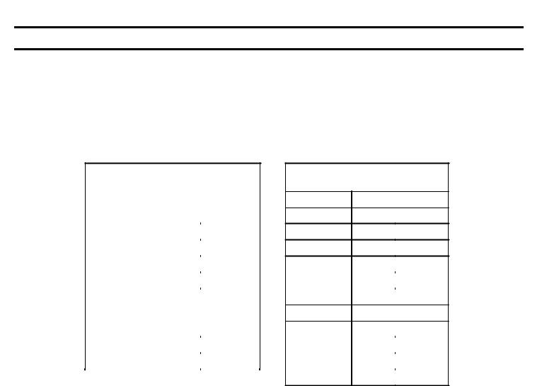
The DSC-S75, DSC-S85 and DSC-F707 cameras are high quality ‘high–end’ cameras with many features, including Carl Zeiss lenses, multi-step and continuous focus, optical and digital zoom, low light auto focus illumination, USB connectivity, JPEG, GIF and TIFF picture formats, burst and bracketed still modes and a MPEG movie mode. The camera specifications are shown in the table:
|
|
|
|
|
MSRP |
999.95 |
599.95 |
499.95 |
|
Imager (Gross) |
1/1.2" 5.2MP Super |
1/1.8" 4.1MP CCD |
1/1.8" 3.3MP CCD |
|
MAD CCD |
||||
|
|
|
||
Effective Pixels |
5.0 Megapixel |
4.0 Megapixel |
3.3 Megapixel |
|
Optical/Digital Zoom |
5X / 2X / 10X |
3X / 2X / 6X |
3X / 2X / 6X |
|
|
|
|
|
|
Carl Zeiss Lens |
Yes |
Yes |
Yes |
|
Lens Thread |
58mm |
52mm w/adapter |
52mm w/adapter |
|
Manual Focus |
Yes, Continuous Ring |
Yes, 13 Step |
Yes, 13 Step |
|
A/D Conversion |
14-bit DXP |
14-bit DXP |
14-bit DXP |
|
AF Illuminator |
Hologram AF |
Yes, On/Off Select |
Yes, On/Off Select |
|
Flash Modes |
Auto/Forced/Off |
Auto/Forced/Off |
Auto/Forced/Off |
|
Red-eye Reduction |
On/Off |
On/Off |
On/Off |
|
LCD/Viewfinder |
1.8" 123K Pixel |
1.8" 123K Pixel |
1.8" 123K Pixel |
|
LCD Backlight |
On/Off, adjustable |
On/Off adjustable |
On/Off adjustable |
|
Recording Media |
Memory Stick only |
Memory Stick only |
Memory Stick only |
|
Still Image Formats |
JPEG, GIF, TIFF |
JPEG, GIF, TIFF |
JPEG, GIF, TIFF |
|
E-mail Mode |
Yes, adds 320x240 |
Yes, adds 320x240 |
Yes, adds 320x240 |
|
Movie Modes |
MPEG EX/HQ |
MPEG EX/HQ |
MPEG EX/HQ |
|
Supplied Storage Media |
16MB Memory Stick |
16MB Memory Stick |
8MB Memory Stick |
|
|
|
|
|
|
Connections |
Video/USB/AC Power |
Video/USB/AC Power |
Video/USB/AC Power |
|
Dimensions |
6-5/6 x 4-7/8 x 2-5/8" |
4-15/16 x 2 x 2-9/16" |
4-15/16 x 2 x 2-9/16" |
|
Weight |
1 lb, 6.4 oz (635g) |
15.2 oz (423g) |
15.2 oz (423g) |
|
Warranty Terms |
1 Year parts, 90 days |
1 Year parts, 90 days |
1 Year parts, 90 days |
|
|
labor |
labor |
labor |
Symbol Explanations
The following symbols used in this manual:
? This symbol in front of a paragraph indicates a helpful service tip or step
N The upraised arm symbol indicates a momentary halt to a process or procedure and evaluate if it is done correctly
X This indicates a caution or warning
1
9. Self-Diagnostics & Screen Display (DA4 & DA-4X Chassis)
Chapter 2 - Software - All Models
All current model Sony still cameras are packaged with a CD containing a USB driver for interfacing with USB computer ports and a number of video editing programs:
∙Two versions of MGI PhotoSuite, a still video editing and album creating application: Version 8.1 for Windows operating systems and version 1.1 for Mac operating systems
∙Also included is MGI Video Wave III, an entry-level motion video editing system.
∙As of this writing, the supplied USB camera driver is version SVP-004. Tables 2-1 and 2-2 list the driver compatibility with Macintosh and Windows operating systems.
Table 2-1 - Windows Operating
Systems
OS Version |
Status |
|
|
3.1 |
X |
|
|
95 |
X |
|
|
98 |
OK |
|
|
98SE |
OK |
|
|
ME |
OK |
|
|
NT3.5.1 |
X |
|
|
NT4.0 |
X |
|
|
2000 PRO |
OK |
|
|
XP PRO |
OK* |
|
|
CE |
X |
|
|
*Driver not needed. Already built into OS
Table 2-2 - Mac Operating
Systems
OS Version Status
7.1.2X
7.5 X
7.6.1X
8.0 |
X |
8.1 |
X |
|
|
8.5 |
X |
8.5.1OK
8.6 |
OK |
9.0 |
OK |
|
|
9.1 |
OK |
|
|
X (10) |
OK* |
X= Not Compatible
The SVP-004 USB device driver is included as an accessory with each camera. It can be downloaded from the Sony web support site at:
http://www.ita.sel.sony.com/support/dvimag/cybershot/
PTP (Picture Transfer Protocol)
∙Picture data is transferred from the camera to a computer via the USB port using PTP (Picture Transfer Protocol).
∙PTP is an open standards protocol for transferring pictures from digital cameras to computers using the USB port
∙PTP protocol allows the camera to be seen by the computer as a mass storage device. When connected to a computer, the computer will see the picture files in the camera as data files.
∙PTP allows only picture objects to be seen and transferred between the camera and the computer. When the memory stick is installed in the camera, non picture files that are stored on the memory stick will not be seen by the computer.
∙PTP works only with Windows XP. It is not supported by any earlier operating system.
2
3. DSC-S75 and DSC-S85 Digital Cameras
Chapter 3 - DSC-S75 and DSC-S85 Digital Cameras
Overview
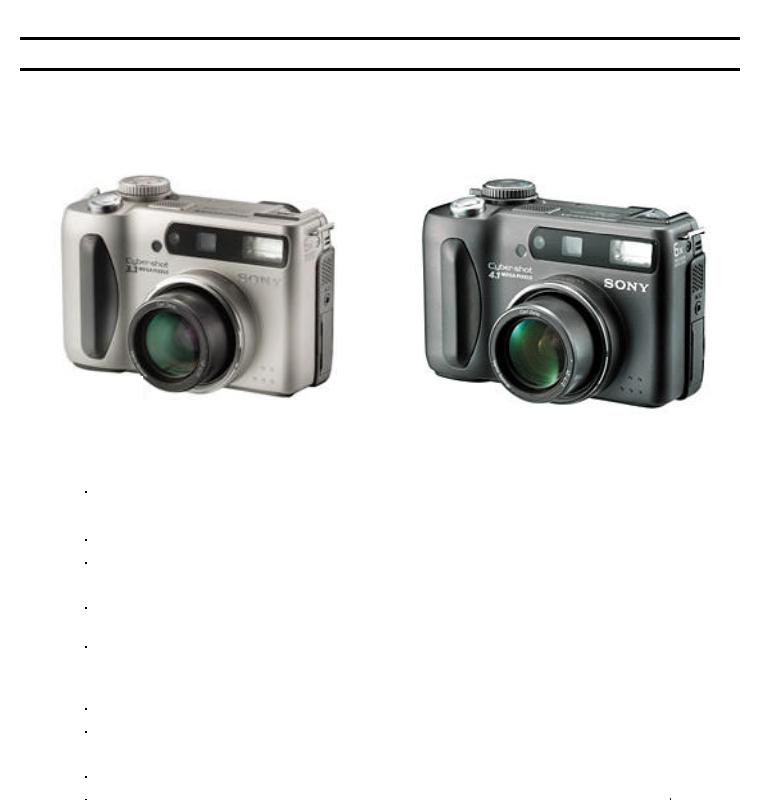
The DSC-S75 and S85 Cyber-shot® digital cameras are very similar in appearance and operation. The circuit descriptions and repair procedures are also very similar and apply equally to both models. The differences are in the body colors (S85 is black and S75 is silver), the number of CCD pixels and the price. The S75 is supplied with an 8 MB Memory Stick ™ and the S85 with a 16 MB memory stick.
DSC-S75 |
DSC-S85 |
|
Repair Tools and Jigs
Repairing these digital cameras requires the following specialized tools and jigs. See Table 3-1 below:
Table 3-1 – Repair Tools and Jigs |
|
|
|
|
|
Jig or Tool |
Vendor |
|
|
|
|
NTSC color monitor |
Your choice |
|
|
|
|
Vectorscope |
Your choice |
|
|
|
|
Radar W jig |
J-6082-429-A |
|
|
|
|
Radar Jig Software |
Available Online at |
|
|
http://service.sel.sony.com/ |
|
|
|
|
Computer to run Radar W software |
Must have USB & bi-direction parallel |
|
|
printer port |
|
|
|
|
RM-95 Adjusting Remote Commander |
J-6082-053-B |
|
|
|
|
CPC 9 interface jig See note 1. |
J-6082-393-C See note 1. |
|
Light box with focus and color bar patterns |
Your choice |
|
|
|
|
Tripod |
Your choice |
|
|
|
|
Tool to discharge flash capacitor |
Made with 1000 ohm 1 watt resistor |
|
|
|
|
Note 1: Do not use earlier version of CPC-9 interface jigs. Use only -393-C version. Earlier versions will damage the SY-68 board. The version and part numbers are silk screened on the CPC-9 jigs.
3

3. DSC-S75 and DSC-S85 Digital Cameras
Alignment
When to Align
Cameras will need alignment when one of the following components is replaced:
∙SY-68 board
∙Lens assembly
∙Flash
∙LCD display
∙LCD character display
Table 3-2 shows the areas that will need realignment when one of the above components is replaced.
Table 3-2 - Adjustment Table
SY-68 |
LCD |
LCD |
FLASH |
BOARD |
LENS DISPLAY BACKLITE |
||
INITIALIZATION OF D PAGE DATA
INITIALIZATION OF 7,9,B,E,F PAGE DATA
VIDEO SYNC LEVEL ADJ.
VIDEO BURST LEVEL ADJ.
FLANGE BACK ADJ.
F No. STANDARD DATA INPUT
MECHANICAL SHUTTER ADJ.
LIGHT LEVEL ADJ.
MIXED COLOR CANCEL ADJ.
AUTO WHITE BALANCE STANDARD DATA INPUT
AUTO WHIT BALANCE ADJ.
COLOR REPRODUCTION ADJ.
CCD (WHITE AND BLACK0 DEFECT COMPENSATION
STROBE WHITE BALANCE ADJ.
LCD INITIAL DATA INPUT
LCD VCO ADJ.
LCD D RANGE ADJ.
LCD BRIGHT ADJ.
LCD CONTRAST ADJ.
LCD COLOR ADJ.
LCD V-COM LEVEL ADJ.
LCD V-COM ADJ.
LCD WHITE BALANCE ADJ
4

3. DSC-S75 and DSC-S85 Digital Cameras
Radar W and RM-95
Alignments should be done with the RADAR W interface jig and associated software. They can also be done with the Adjustment RM-95 remote control jig, but RADAR W is an order of magnitudes faster than the Service RM-95, and unlike the RM-95, it is less prone to data entry mistakes.
The Sony part number for the Radar W interface jig is J-6082-429-A.
The RM-95 jig should be reserved for making small registry changes or for checking the operation of the camera switches.
The diagrams show how to interconnect the interface jig between the camera and the RM-95 or the Radar W jig.
FROM |
+ |
- |
|
CAMERA |
|
ADJUSTING |
INTERFACE UNIT |
|
1 |
REMOTE |
|
|
COMMANDER |
J-6082-429-A |
|
|
|
||
|
|
RM-95 |
|
TO
COMPUTER
PARALLEL
PORT
|
|
REPLACE RM-95 PLUG |
|
|
|
CPC-9 JIG |
|
WITH INTERFACE |
J-6082-393-C |
|
UNIT PLUG |
|
INTERFACING RM-95 OR RADAR W JIG |
|
5

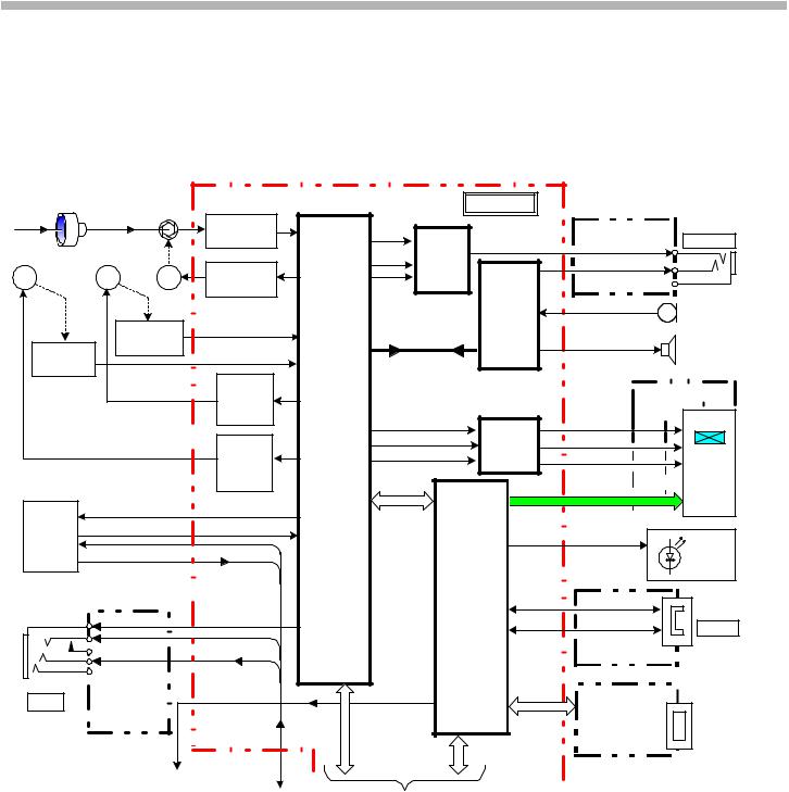
4. DSC-75 and DSC-S85 Block Diagram
Chapter 4 - DSC-S75 and DSC-S85 Block Diagram
The following is a short explanation of the internal camera operations in block diagram format, based on the SY68 board as the central item.
Overview
Refer to Figure 4-1. Most of the camera functions are concentrated on SY-68 board, including interfaces for external switches, controls and I/O interfaces to the outside world. The power supply is on the DM-101 board.
Operation
The camera is controlled by three processors: CAMERA DSP IC301, FRONT CONTROL IC402 and MC CAMERA SH DSP IC501. The video to the LCD panel and a power supply DC CONTROL IC.
∙The CAMERA DSP converts the light image falling on the CCD into video signals for the LCD monitor and A/ V jack and into digital video data for the memory stick and USB port.
∙The Front Control IC acts as an I/O interface. It processes all input commands from the camera switches dials and sensors, controls the flash charging and generates the characters for the LCD monitor panel and the LCD readout display.
∙The MC Camera SH DSP IC controls the digital data to the LCD monitor panel (the video signals are controlled by the Camera DSP) and the USB I/O.
∙The DC Control IC controls all of the regulated power supply outputs from the DM-101 board.
Accessory jack J782 interfaces with the camera LANC data and is also used for triggering an external flash.
CN753 is the Memory Stick™ socket
SY-68 Board Troubleshooting
The SY-68 board is not a repairable item. If defective, it should be replaced and the old board returned for core credit, as per Sony policy.
The board, together with the lens assembly, is easily removable once the back cover is taken off. They are held in place by just five easily visible screws; no further explanation is necessary.
NThe camera must be fully aligned after the board is replaced. This includes flange back adjustment. To reduce the alignment time, whenever possible use Radar W to upload and save the data from the original SY board to the computer then download it back into the new board.
?If camera is intermittent, check the SY board for flatness. Replace if it is slightly bowed along its long axis.
?After replacing a SY-68 board, the camera may display Japanese characters. Use the Service RM-95 to change the display to English. Change the data in page D, address 4F, to 04 (do not forget to disable write protect before writing and to press Pause after writing). You can also use this method if the user inadvertently changes the display to another language.
6
4. DSC-75 and DSC-S85 Block Diagram
|
|
|
|
|
|
|
|
|
SY-68 BD. |
|
|
|
|
|
|
|
IMAGER |
|
Y |
|
|
JK-211BD. |
|
|
|
|
|
|
PROCESS |
|
|
VIDEO OUT |
AV OUT |
||
|
ZOOM |
|
|
|
VIDEO |
||||||
|
|
|
|
C |
|
|
|||||
|
|
|
|
|
|
|
|||||
|
|
SHUTTER |
|
AMP |
|
|
|
||||
M |
FOCUS |
M |
IRIS |
M |
|
|
|
AUDIO OUT |
|
||
DRIVE |
|
V |
|
|
|
||||||
|
|
|
|
|
|
|
AUDIO |
|
|||
|
|
|
|
|
|
|
|
|
|
|
|
|
|
|
|
|
Z SENS RST |
|
|
|
PROC. |
|
MIC. |
|
|
|
SENSOR |
|
|
|
& AMP. |
|
|
||
|
|
|
|
|
|
|
|
|
SPEAKER |
||
|
SENSOR |
|
|
|
FSENS RST |
|
|
|
|
|
|
|
|
|
|
|
|
|
|
|
|
||
|
|
|
|
|
ZOOM |
|
|
|
|
CK-103 BOARD |
|
|
|
|
|
|
MOTOR |
IC301 |
|
|
|
||
|
|
|
|
|
|
|
|
|
|
||
|
|
|
|
|
DRIVE |
|
|
|
|
|
|
|
|
|
|
|
CAMERA |
|
|
|
VR |
LCD901 |
|
|
|
|
|
|
|
|
|
LCD |
|||
|
|
|
|
|
FOCUS |
DSP |
|
|
VG |
|
|
|
|
|
|
|
|
|
|
DRIVE |
|
||
|
|
|
|
|
|
|
|
VB |
|
||
|
|
|
|
|
MOTOR |
|
|
|
COLOR |
||
|
|
|
|
|
|
|
|
|
|||
|
|
|
|
|
|
|
|
|
|
||
|
|
|
|
|
DRIVE |
|
|
|
|
|
|
|
|
|
|
|
|
|
|
|
|
LCD |
|
|
|
|
|
|
|
|
|
|
|
|
|
|
|
|
|
|
STRB ON |
|
|
|
|
|
MON. |
|
|
|
|
|
|
|
|
|
|
|
|
STRB AIN
FLASH
|
STB CHARGE |
|
|
|
BACK |
|
XSTB FULL |
|
IC501 |
|
LIGHT |
|
|
|
|
|
|
|
EXT STRB ON |
MC |
USB D+ |
|
|
|
CAMERA |
|
|||
|
USB D- |
USB |
|||
|
|
|
SH DSP |
||
|
|
|
|
||
|
LANC SIG. |
|
JK-211BOARD |
|
|
|
LANC DC |
|
|
||
J782 |
|
|
|
||
JK-211 |
|
|
|
|
|
ACC |
|
|
DM-101 |
|
|
BOARD |
|
|
|
||
|
|
CLK |
CN753 |
||
|
|
|
BOARD |
||
|
|
|
|
MEMORY |
|
|
|
|
|
|
|
|
|
|
|
|
STICK |
|
IC001 |
|
|
|
SOCKET |
|
|
|
|
|
|
|
DC CONT. |
TO/FROM FRONT CONTROL IC |
|
|
|
|
|
FIGURE 4-1 - OVERALL BLOCK DIAGRAM A |
4.1DSC02a 1483 10/10/02 |
||
7
4. DSC-75 and DSC-S85 Block Diagram
|
|
|
TO/FROM |
|
|
|
TO/ FROM |
|
|
MC CAMERA |
|
|
|
|
|
SH DSP |
|
|
|
|
FLASH UNIT & |
|
|
|
|
||
TO/FROM |
|
|
|
|||
LANC |
|
|
|
|
||
|
CAMERA |
|
|
|
||
ACC |
|
|
|
|
||
|
|
DSP |
|
|
|
|
|
|
|
|
|
|
|
|
|
|
|
|
CK-103 |
KY-55 BOARD |
|
|
|
|
|
|
|
|
|
|
KEY AD 0-2 |
BOARD |
FUNCTION |
|
JK-211 |
|
|
|
KEY |
||
|
|
|
|
|
||
BOARD |
|
|
|
|
|
|
LITHIUM |
VL 3V |
INITIAL |
|
|
|
CONTROL SW |
BATT. |
|
RESET |
|
|
|
|
|
|
|
|
BLOCK (MODE |
||
|
|
BACK-UP |
|
|
|
|
|
|
|
|
|
SHUTTER |
|
|
|
|
|
|
|
|
|
|
DM-101 BD. |
|
|
|
SWITCH |
+ |
|
|
|
|
MODE |
|
|
|
|
|
|
||
BATT. |
|
BATT. SIG. |
IC402 |
|
|
DIAL |
TERM. S |
|
|
|
|
POWER |
|
- |
|
SYSDD ON |
FRONT |
|
|
|
|
|
D1.8V |
CONTROL |
|
|
ON/OFF |
|
|
|
|
|
|
|
|
|
D3.2V |
|
COM 0-3 |
|
|
|
|
CAM 3.2V |
|
|
|
|
|
IC001 |
A 3.2V |
|
SEG 0-19 |
|
|
|
CAM P 5V |
|
|
LCD |
||
|
DC |
A 4.9V |
|
|
|
CHARACTER DISP. |
|
CONT. |
P 4.9V |
|
|
|
|
|
|
10.05V |
|
KEY AD3 |
|
ZOOM |
|
|
15.05V |
|
|
||
|
|
-10.05V |
|
|
|
SWITCH |
|
|
PANEL-15.3V |
|
DIAL A,B |
|
JOG DIAL |
DC IN |
|
CAM -7.5V |
|
|
|
|
|
|
|
CONTROL SW. |
|||
|
|
|
|
|||
|
ACV UNREG |
|
|
|||
|
|
|
BLOCK ZOOM |
|||
|
ST UNREG |
SY-68 BOARD |
|
|
|
|
|
|
BATT.UNREG |
|
|
|
|
|
|
|
|
|
|
|
FIGURE 4-2 - OVERALL BLOCK DIAGRAM B |
4.2DSC02b 1483 10/1 |
8
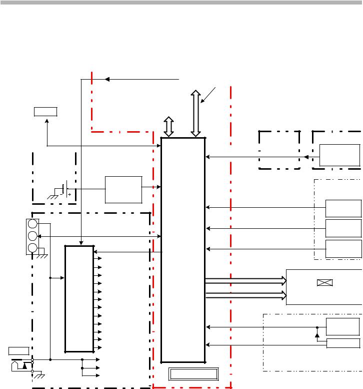
5. DSC-S75 and DSC-S85 Power Supply
Chapter 5 - DSC-S75 and DSC-S85 Power Supply
The DM-101 Power Supply board converts the dc input from the ac adapter or battery into all of the necessary ac and ±dc voltages.
BoardAccess
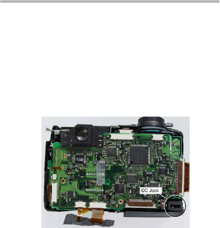
The DM-101 board is sandwiched between the SY-68 board and the front of the camera and is not easily accessible for live troubleshooting.
The output and control lines to the board can be checked at CN701 on the SY-68 board when the camera back is removed. Although the camera will not operate properly with the back removed, the power supply will power up. The picture shows the location of CN701 on the SY-68 board.
Circuit Operation
Figure 5-1 shows a block diagram of the power supply board. Due to limited access, “live” troubleshooting is limited to the CN701 connector on the SY-68 board. Therefore, the circuit description of the DM-101 board will be limited to a block diagram.
With the exception of an unregulated always-on voltage and an unregulated battery voltage, all voltages are produced by discrete switching circuits on the board. The switching circuits are controlled and regulated by DC Control IC001, which provides the switching signals and feedback control to the switching transistors.
9

5. DSC-S75 and DSC-S85 Power Supply
CN001 |
|
|
|
|
BATT. ON |
39 |
7 |
CN701 |
|||
|
F004 |
F005 |
|
ALWAYS ON |
|||||||
|
1 |
|
|
35 |
11 |
|
|||||
|
|
F003 |
|
|
|
|
|
|
|||
|
2 |
|
|
VCC-B |
VCC-C |
|
|
|
|||
J001 |
3 |
|
F001 |
|
|
|
|
||||
|
|
|
|
|
|
33 |
|
|
|||
|
|
F002 |
VCC-A |
|
|
|
17 |
|
|||
DC IN |
|
|
|
|
|
|
|||||
|
|
|
|
|
34 |
13 |
|
||||
|
Q002 |
|
VCC-D |
|
|
A 3.2V |
28 |
17 |
|
||
|
FAST |
|
|
|
Q009 |
CAM 3.2V |
29 |
18 |
|
||
|
CH. |
|
|
|
26 |
19 |
|
||||
|
|
|
|
3.2V CAM |
|
||||||
|
|
|
|
|
|
|
|
|
|||
|
|
|
|
|
SW. REG. |
|
|
|
27 |
20 |
|
|
|
|
|
SW |
|
D 3.2V |
|
|
|
||
|
|
|
|
|
|
23 |
21 |
|
|||
Q003,004 |
|
|
|
|
|
|
|||||
|
|
VCC-D |
FB |
|
|
25 |
23 |
|
|||
|
INIT. |
|
|
|
|
|
|
|
|||
|
|
|
|
|
|
|
|
|
|
|
|
|
CH. |
|
|
|
|
|
|
|
|
|
|
|
CN002 |
D003 |
|
|
Q007 |
|
A 4.9V |
12 |
32 |
|
|
|
|
|
CAM |
|
|
||||||
+ |
|
|
|
|
|
|
|
||||
1 |
|
|
|
|
|
|
14 |
34 |
|
||
|
|
|
SW. REG. |
|
|
|
SY-68 BD. |
||||
S |
2 |
|
|
SW |
|
P4.9V |
|||||
|
|
|
|
|
|||||||
BATT |
|
|
|
11 |
35 |
|
|||||
- |
3 |
|
FB |
|
|
|
|
|
|||
SIG. |
|
|
|
|
|
|
|
|
|||
|
|
|
|
|
|
|
|
|
|
|
|
|
BT902 |
|
|
|
4.9V |
|
|
|
|
|
|
|
BATT. |
|
|
VCC-B |
|
|
10V |
|
|
|
|
TERMINAL |
|
|
|
Q005 |
|
|
19 |
27 |
|
||
|
|
|
|
|
15V |
|
|||||
|
|
|
|
|
|
|
|
|
|
||
|
|
|
|
|
+10V |
|
|
18 |
28 |
|
|
|
|
|
|
|
|
|
-10.5V |
|
|||
|
|
|
|
|
+15V |
|
|
17 |
29 |
|
|
|
|
|
|
|
|
|
|
|
|||
|
|
|
IC001 |
SW |
-10.5V |
|
|
V. REF. |
|
|
|
|
|
|
DC |
|
|
|
|
|
|
||
|
|
SCP |
|
FB |
|
|
|
|
|
||
|
|
CONTROL |
|
|
|
|
|
|
|
||
|
|
|
VCC-B |
|
|
|
|
|
|
|
|
|
|
|
|
|
|
|
CAM |
|
|
|
|
|
|
|
|
|
|
V. REF. |
|
16 |
30 |
|
|
|
|
SYS |
|
|
|
|
|
-7.5V |
|
|
|
|
|
|
|
|
|
|
|
|
|
|
|
|
|
DD ON |
|
|
Q008 |
|
|
PANEL |
|
|
|
|
|
|
|
SW |
BACK |
|
|
|
|
|
|
|
|
|
|
Q070. |
|
-15.3V |
|
|
|
||
|
|
|
|
LIGHT |
|
|
|
|
|||
|
|
|
|
|
|
15 |
31 |
|
|||
|
|
|
|
|
Q076 |
|
|
|
|||
|
|
|
|
|
-VOL |
|
|
7 |
39 |
|
|
|
|
|
|
|
-15V |
|
|
|
|||
|
|
|
|
VCC-A |
|
|
ON/OFF |
|
|||
|
|
|
|
|
SW. REG. |
|
|
|
|||
|
|
|
|
|
BL VO- |
|
|
|
|||
|
|
MD-101 |
|
|
|
|
|
31 |
15 |
|
|
|
|
|
|
|
|
|
|
|
|||
|
|
BOARD |
|
|
Q011, |
|
|
D 1.8V |
8 |
36 |
|
|
|
|
|
|
|
|
SCP |
10 |
38 |
|
|
|
|
|
|
|
Q012 |
|
|
|
|||
|
|
|
|
|
|
SYS DD ON |
30 |
16 |
|
||
|
|
|
|
SW |
1.8B |
|
32 |
14 |
|
||
|
|
|
|
|
BATT SIG |
|
|||||
|
|
|
|
SW |
SW. REG. |
|
40 |
6 |
|
||
|
|
|
|
|
|
|
INIT CH. ON |
|
|||
|
|
|
|
|
|
FB |
36 |
10 |
|
||
|
|
|
|
|
|
|
FAST CH. |
|
|||
|
|
|
|
|
|
|
|
|
|||
|
|
|
|
|
|
|
|
37 |
9 |
|
|
|
|
|
|
V. REF. |
|
BATT. /XEXT |
|
||||
|
|
|
|
|
38 |
8 |
|
||||
|
|
FIGURE 5-1 - POWER SUPPLY BLOCK DIAGRAM 1DSC02 1479 |
|
||||||||
|
|
10/11/02 |
|
|
|||||||
10
5. DSC-S75 and DSC-S85 Power Supply
Unregulated always ON voltages
The always-on voltage is fed to all circuits via four fuses ? F1 ~ F4. Each fuse supplies a different section of
IC001 and its respective external VCC-B switching circuit.
+10V, +15V, -10V Supplies |
FROM |
The circuit supplying these voltages |
IC001 |
|
|
is unique: one of the secondary |
|
windings is in series with the +4.9V |
|
output from Q007. See Figure 5-2. It |
|
operates as follows: |
|
1.The primary winding of the transformer is switched by Q005 to provide an ac voltage to the
primary. Q005 is powered by Vcc-B.
|
|
-10.5V |
Q005 |
+ |
|
|
|
|
SW. |
+ |
+15V |
|
|
|
|
PRI |
|
|
+ |
+10V |
|
|
4.9V FROM
Q007
FIGURE 5-2 - +10V, +15V,-10.5V DIAGRAM 9DSC02 1493 9/26/02
2.The turn ratio of the secondary +10V and +15V winding can provide only +5V and +10V. To get the additional 5 volts, the common leg of the secondary winding is not connected to ground but to the +4.9V line from Q007. This causes the output from this secondary winding to increase by 4.9V.
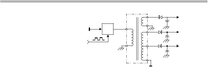
V REF
This output line from Control IC001 provides a very stable 1.5 reference voltage to many of the voltage regulators in the power supply.
DC IN – Battery Switching
AC Adapter Connected
See Figure 5-1.
∙The ac adapter directly supplies the camera with power when it is connected. Q002 provides a fast charge (initial charge) to the battery if the battery charge is low.
∙Q003, Q004 and D003 charges the battery with a slow initial charge (current limiting)
∙Once the battery has charged up a little, switch Q003 / Q004 opens and Q002 closes. This provides the battery with a faster charge.
∙When the battery has fully charged, switch Q002 opens and the battery is isolated from the ac adapter power.
AC adapter Not Connected
See Figure 5-1.
∙The battery supplies power to fuses F001 ~ F004 via switch Q003/Q004 and D003.
11

5. DSC-S75 and DSC-S85 Power Supply
Control Circuits
See Figure 5-1
The control lines for this power supply are:
SYS DD ON
This is the master switch that turns the DC Control IC ON/OFF. The line must be HIGH (3.2v) for the IC to operate. It is controlled by the SY-68 board.
SCP (Short Circuit Protection)
See Figure 5-3
This is the short circuit protection line. The SY-68 board monitors the -10.5V and +15 volt lines and will output a LOW on the SCP line if the voltages it monitors drops to -8.5 volts and +12 volts, respectively.
DC BATT./ |
F004 |
|
|
|
|
|
|
ADAPTER |
|
|
|
|
|
||
F003 |
|
|
|
|
|
||
INPUT |
|
|
|
|
|
||
F001 |
|
|
|
|
|
||
DM-101 |
|
|
|
|
|
||
F002 |
|
|
|
|
|
||
BOARD (1/2) |
|
|
|
|
|
||
|
|
|
|
|
|
|
|
|
VCC 63 |
|
|
|
|
|
|
|
VCC 42 |
15V |
18 |
28 |
15V |
|
|
|
VCC |
51 |
-10.5V |
|
|
||
|
17 |
29 |
|
|
|||
|
VCC 28 |
|
|
|
|||
|
|
|
-10.5V |
|
|||
|
IC001 |
|
|
|
|
|
CAM 15V |
|
DC |
|
|
|
|
|
|
|
|
|
|
|
|
|
|
CONTROL |
|
|
|
|
|
|
|
SCP |
|
64 |
|
|
|
|
|
|
|
|
|
|
|
|
|
13 |
|
|
|
|
|
|
|
SYS |
|
50 |
|
|
|
|
|
OUT |
|
PULSE |
|
|
|
|
|
DD ON |
|
|
|
|
|
||
SC |
|
OUTPUTS |
|
|
|
|
|
30 |
56 |
|
|
|
|
||
|
TL1 |
|
|
|
|
|
|
29 |
SC |
4 |
|
|
|
Q062, 063 |
|
|
|
|
|
EMERGENCY |
SY-68 BOARD 1/2 |
||
|
|
|
|
|
|||
|
TL2 |
|
SCP |
30 |
SCP |
DETECT |
|
|
|
|
|
16 |
|
|
|
|
|
|
SYS DD ON |
|
|
|
SYS DD ON |
|
|
|
32 |
14 |
|
|
|
|
|
|
|
|
|
||
FIGURE 5-3 - SAFETY SHUTDOWN CIRCUIT (SCP) |
2DSC02 1480 10/11/02 |
12
5. DSC-S75 and DSC-S85 Power Supply
Power Supply Troubleshooting
NDo not repair any of the printed circuit boards on units under warranty. If defective, order a new one and send the old one back for a refund of the core charge, as per Sony policy.
Troubleshooting the DM-101 power supply board is limited to checking the output voltage levels and control signal lines on SY-68 connector CN701 and to checking fuses and other components with the board removed.
∙If the camera is dead, the most important voltage to check is the always-on voltage from fuse F004. See Figure 5-1. Since this fuse provides always-on power to the SY-68 board, that board will not be able to provide a HIGH to the SYS DD ON line and the power supply will not turn on.
Failure to diagnose this fuse can prevent the technician from determining which board is defective.
Replace the DM-101 board if this fuse is open after first making sure that there is not a short in the SY-68 board that is blowing the fuse.
∙If the lack of a particular output voltage is traced to a blown fuse, make sure to also check the switching transistors that it feeds for a short.
?A common complaint of the battery not charging or unit not running from ac adaptor is caused by a physically damaged ac adapter jack. Check this jack before replacing the battery or ac adapter. It is easily lifted out once the back cover is removed. The part number is for the jack is 1-7940-456-1. See Figure 5-4.
Figure 5-4
13
Loading...