


 Loading...
GSM TELEPHONE
SGH-D820
|
JVP WHOHSKRQH |
|
|
FRQWHQWV |
|
|
|
|
|
|
|
|
|
|
1. |
Specification |
|
|
|
|
|||
|
|
|
2. |
Circuit Description |
|
|
|
|
3. |
Exploded Views and Parts List |
|
|
|
|
4. |
Electrical Parts List |
|
|
|
|
5. |
Block Diagrams |
|
|
|
|
6. |
PCB Diagrams |
|
|
|
|
7. |
Flow Chart of Troubleshooting |
|
|
|
|
|
|
|
|
|
|
|
|
|

This Service Manual is a property of Samsung Electronics Co.,Ltd. Any unauthorized use of Manual can be punished under applicable International and/or domestic law.
Samsung Electronics Co.,Ltd. March. 2006 Printed in Korea.
Code No.: GH68-09648A BASIC.

1. Specification
1-1. GSM General Specification
|
GSM850 |
GSM900 |
EGSM 900 |
DCS1800 |
PCS1900 |
|
|
Phase 1 |
Phase 2 |
Phase 1 |
|||
|
|
|
||||
|
|
|
|
|
|
|
Freq. |
824~849 |
890~915 |
880~915 |
1710~1785 |
1850~1910 |
|
Band[MHz] |
||||||
869~864 |
935~960 |
925~960 |
1805~1880 |
1930~1990 |
||
Uplink/Downlink |
||||||
|
|
|
|
|
||
ARFCN range |
128~251 |
1~124 |
0~124 & |
512~885 |
512~810 |
|
975~1023 |
||||||
|
|
|
|
|
||
|
|
|
|
|
|
|
Tx/Rx spacing |
45MHz |
45MHz |
45MHz |
95MHz |
80MHz |
|
|
|
|
|
|
|
|
Mod. Bit rate |
270.833kbps |
270.833kbps |
270.833kbps |
270.833kbps |
270.833kbps |
|
/ Bit Period |
3.692us |
3.692us |
3.692us |
3.692us |
3.692us |
|
|
|
|
|
|
|
|
Time Slot |
576.9us |
576.9us |
576.9us |
576.9us |
576.9us |
|
Period |
||||||
4.615ms |
4.615ms |
4.615ms |
4.615ms |
4.615ms |
||
/ Frame Period |
||||||
|
|
|
|
|
||
|
|
|
|
|
|
|
Modulation |
0.3GMSK |
0.3GMSK |
0.3GMSK |
0.3GMSK |
0.3GMSK |
|
|
|
|
|
|
|
|
MS Power |
33dBm~5dBm |
33dBm~5dBm |
33dBm~5dBm |
30dBm~0dBm |
30dBm~0dBm |
|
|
|
|
|
|
|
|
Power Class |
5pcl ~ 19pcl |
5pcl ~ 19pcl |
5pcl ~ 19pcl |
0pcl ~ 15pcl |
0pcl ~ 15pcl |
|
|
|
|
|
|
|
|
Sensitivity |
-102dBm |
-102dBm |
-102dBm |
-100dBm |
-100dBm |
|
|
|
|
|
|
|
|
TDMA Mux |
8 |
8 |
8 |
8 |
8 |
|
|
|
|
|
|
|
|
Cell Radius |
35Km |
35Km |
35Km |
2Km |
2Km |
|
|
|
|
|
|
|
1-1
SAMSUNG Proprietary-Contents may change without notice
This Document can not be used without Samsung's authorization

Specification
1-2. GSM TX power class
|
TX Power |
|
|
TX Power |
|
|
TX Power |
|
|
TX Power |
|
|
|
control |
GSM850 |
|
control |
GSM900 |
|
control |
DCS1800 |
|
control |
PCS1900 |
|
|
level |
|
|
level |
|
|
level |
|
|
level |
|
|
|
5 |
33±3 dBm |
|
5 |
33±3 dBm |
|
0 |
30±3 dBm |
|
0 |
30±3 dBm |
|
|
|
|
|
|
|
|
|
|
|
|
|
|
|
6 |
31±3 dBm |
|
6 |
31±3 dBm |
|
1 |
28±3 dBm |
|
1 |
28±3 dBm |
|
|
|
|
|
|
|
|
|
|
|
|
|
|
|
7 |
29±3 dBm |
|
7 |
29±3 dBm |
|
2 |
26±3 dBm |
|
2 |
26±3 dBm |
|
|
|
|
|
|
|
|
|
|
|
|
|
|
|
8 |
27±3 dBm |
|
8 |
27±3 dBm |
|
3 |
24±3 dBm |
|
3 |
24±3 dBm |
|
|
|
|
|
|
|
|
|
|
|
|
|
|
|
9 |
25±3 dBm |
|
9 |
25±3 dBm |
|
4 |
22±3 dBm |
|
4 |
22±3 dBm |
|
|
|
|
|
|
|
|
|
|
|
|
|
|
|
10 |
23±3 dBm |
|
10 |
23±3 dBm |
|
5 |
20±3 dBm |
|
5 |
20±3 dBm |
|
|
|
|
|
|
|
|
|
|
|
|
|
|
|
11 |
21±3 dBm |
|
11 |
21±3 dBm |
|
6 |
18±3 dBm |
|
6 |
18±3 dBm |
|
|
|
|
|
|
|
|
|
|
|
|
|
|
|
12 |
19±3 dBm |
|
12 |
19±3 dBm |
|
7 |
16±3 dBm |
|
7 |
16±3 dBm |
|
|
|
|
|
|
|
|
|
|
|
|
|
|
|
13 |
17±3 dBm |
|
13 |
17±3 dBm |
|
8 |
14±3 dBm |
|
8 |
14±3 dBm |
|
|
|
|
|
|
|
|
|
|
|
|
|
|
|
14 |
15±3 dBm |
|
14 |
15±3 dBm |
|
|
|
|
|
|
|
|
|
|
9 |
12±4 dBm |
|
9 |
12±4 dBm |
|
||||
|
|
|
|
|
|
|
|
|
|
|
|
|
|
15 |
13±3 dBm |
|
15 |
13±3 dBm |
|
10 |
10±4 dBm |
|
10 |
10±4 dBm |
|
|
|
|
|
|
|
|
|
|
|
|
|
|
|
16 |
11±5 dBm |
|
16 |
11±5 dBm |
|
11 |
8±4dBm |
|
11 |
8±4dBm |
|
|
|
|
|
|
|
|
|
|
|
|
|
|
|
17 |
9±5 dBm |
|
17 |
9±5 dBm |
|
12 |
6±4 dBm |
|
12 |
6±4 dBm |
|
|
|
|
|
|
|
|
|
|
|
|
|
|
|
18 |
7±5 dBm |
|
18 |
7±5 dBm |
|
13 |
4±4 dBm |
|
13 |
4±4 dBm |
|
|
|
|
|
|
|
|
|
|
|
|
|
|
|
19 |
5±5 dBm |
|
19 |
5±5 dBm |
|
14 |
2±5 dBm |
|
14 |
2±5 dBm |
|
|
|
|
|
|
|
|
|
|
|
|
|
|
|
|
|
|
|
|
|
15 |
0±5 dBm |
|
15 |
0±5 dBm |
|
|
|
|
|
|
|
1 |
-2 |
|
|
|
|
|
|
|
|
|
|
|
|
|
|
|
|
|
|
SAMSUNG Proprietary-Contents may change without notice
This Document can not be used without Samsung's authorization

2. Circuit Description
2-1. SGH-D820 RF Circuit Description
2-1-1. RX PART
- FRONT END MODULE(ANTENNA SWITCH MODULE + RX SAW FILTER) (F101)
It performs to switch Tx & Rx paths for GSM850, GSM900, DCS1800 and PCS1900 with logic controls below.
- FEM Control Logic Table
|
FESW1 |
FESW2 |
FESW2 |
|
|
|
|
Tx Mode (GSM850/900) |
H |
L |
L |
|
|
|
|
Tx Mode (DCS1800/1900) |
L |
H |
L |
|
|
|
|
Rx Mode (GSM900/850) |
L |
L |
L |
|
|
|
|
Rx Mode (DCS1800) |
L |
L |
L |
|
|
|
|
Rx Mode (PCS1900) |
L |
L |
H |
|
|
|
|
- VC-TCXO (TCX100)
This |
module generates the 26MHz reference clock to drive the logic and RF systems. |
It is |
turned on when the supply voltage (+VCC_SYN) is applied. |
After buffering, the 26MHz reference clock is supplied to the other parts of the system through the transceiver pin |
|
CLKOUT. |
|
- Transceiver (U102)
This chip is fully integrated GSM & GPRS quad-band transceiver with RF VCO, loop filters and most of the passive components required in it.
It also fully integrated fractional N RF synthesizer with AFC control possibility, RF VCO with integrated supply regulator. Semi integrated reference oscillator with integrated supply regulator.
RF Receiver front-end amplifies the E-GSM900(GSM850), DCS1800 and PCS1900 aerial signal, convert the chosen
channel down to a low IF of 100kHz. |
|
In IF |
section, further amplifies the wanted channel, performs gain control to tune the output level to the desired value and |
rejects |
DC. |
2-1-2. TX PART
The transmitter is fully differential using a direct up conversion architecture. It consists of a signal side band
power |
up mixer. Gain is controlled by |
6 dB via 3-wire serial bus programing. The fully integrated VCO and power |
mixer |
achieve LO suppression, quadrature phase error, quadrature amplitude balance and low noise floor specification. |
|
Output |
matching/balun components drive |
a standard 50 ohms single ended load. |
2-1
SAMSUNG Proprietary-Contents may change without notice
This Document can not be used without Samsung's authorization

Circuit Description
2-2. Baseband Circuit description of SGH-D820
2-2-1. PCF50603 (U400)
-Power Management
Eight low-dropout regulators designed specifically for GSM applications power the terminal and help ensure optimal system performance and long battery life. A programmable boost converter provides support for 1.8V, 3.0V SIMs, while a self-resetting, electronically fused switch supplies power to external accessories. Ancillary support functions, such as RTC module and High Voltage Charge pump, Clock generator, aid in reducing both board area and system complexity.
I2C BUS serial interface provides access to control and configuration registers. This interface gives a microprocessor full control of the PCF50603 and enables system designers to maximize both standby and talk times.
Supervisory functions. including a reset generator, an input voltage monitor, and a temperature sensor, support reliable system design. These functions work together to ensure proper system behavior during start-up or in the event of a fault condition(low microprocessor voltage, insufficient battery energy, or excessive die temperature).
-Pulse-Width Modulator
The Backlight Brightness Modulator (BBM) contains a programmable Pulse-width modulator (PWM) to modulate the intensity of a series of LED's or to control a DC/DC converter that drives LCD backlight.
This phone is using PWM control to modulate the LCD backlight brightness.
-Clock Generator
The Clock Generator (CG) generates all clocks for internal and external usage. The 32.768 kHz crystal oscillator provides an accurate low clock frequency for the PCF50603 and other circuitry.
2-2-2. LCD
D820 has just one 2.12" TFT LCD. 16-bit data lines(LD(0)~LD(15)) transfers data and commands to LCD. There are couple of control signals such as RS, LCD_MAIN_CS, L_WRB, etc. RS stands for "Register Select pin." When RS = 0, data can be written to the index register or status can be read, and when RS = 1, an instruction can be issued or data can be written to or read from RAM. Read or write operation is selected according to L_WRB signals. The data is received when the R/W bit is 0, and is transmitted when the R/W bit is 1. At the falling edge of LCD_MAIN_CS input, serial data transfer is initiated. On the other hand, at the rising edge of LCD_MAIN_CS input, the data transfer is ceased.
2-2-3. Key
Key recognition part is consisted of 8 ports from PCF5213EL1. KEY_ROW(0:4) & KEY_COL(0:4)
These signals performs with the matrix. Any input from the matrix informs the key status to key interface in the PCF5213EL1. Power on/off key is independent of the matrix. Therefore, 'power on/off' signal is directly connected with PCF50603 to turn PCF50603 on.
Two 3.3V LDOs(U716, U823) enable Main and Sub Key LED on. Main and Sub Key LED are controlled by KEYLED_ON and SLIDER_KEY_ON signal respectively.
2-2
SAMSUNG Proprietary-Contents may change without notice
This Document can not be used without Samsung's authorization

Circuit Description
2-2-4. EMI ESD Filter (F500)
This system uses the EMI ESD filter (F500) to protect the device from noises from IF CONNECTOR part.
2-2-5. IF connetor (IFC500)
It has 20-pin. They are designed to allocate not only 'power and data lines'(VBAT, V_EXT_CHARGE, USB_D+, +VBUS, USB_D-, TXD1, RXD1, AUX_ON, EXT1, EXT2 and GND) but also Earphone lines(EAMMIC_P/N, EARSPK_R/L, EAR_SWITCH, EARSPK_COM and EAR_ADC). They connected to power supply IC, microprocessor, signal processor IC and Earphone.
2-2-6. Battery Charge Management
D820 has a complete constant-current/constant-voltage linear charger for single cell lithium-ion batteries inside.
If Travel Adapter is connected, "V_EXT_CHARGE" begins to provide the charger IC (to battery) with power (current). When the charging operation is done, "END_OF_CHG" informs it to PCF5213EL1 to stop the operation. "CHG_ON" signal enables the charger IC to operate in adequate circumstances.
2-2-7. Audio - Part
D820 has several audio-outputs such as stereo speaker, receiver, earphone, etc. HFR P/N signals from CPU are connected to the receiver. MIC_CP/N are connected to the main MIC and MIC_CP2/N2 as well.
SAPA1D2 is a Class-D amplifier for outputting sounds that are used by mobile phones including MP3 playback, melodies, voice output on speaker phone mode and so on..
STG3699(U515) is an analog switch to connect SAPA1D2 input port to main DSP or CODEC Chip.
2-2-8. Memory (UME307)
D820 has KBH10PD00M-D414 as a memory module.
The KBH10PD00M-D414 is a Multi Chip Package Memory which combines 256Mbit Synchronous Burst Multi Bank NOR Flash Memory and 1Gbit OneNAND Flash and 256Mbit Synchronous Burst UtRAM.
It has 16 bit data line, HD[0~15] which is connected to PCF5213 and CL8522S5(Multi-media chip), also has 24 bit address lines, HA[1~24]. There are 3 chip select signals, CS0n_FLASH, CS1n_RAM, and CS4n_NAND.
In the writing process, WEn is fallen to low and it enables writing process to operate. During reading process, OEn is fallen to low and it enables reading process to operate. Each chip select signals in the PCF5213EL1 choose different types of memory.
2-2-9. PCF5213EL1 (UCP200)
The PCF5213EL1 is mainly composed of embeded DSP and ARM core. The DSP subsystem includes the Saturn DSP core with embedded RAM and ROM, and a set of peripherals. It has 24k×16 bits PRAM, 104k×16 bits, 32k×16 XYRAM and 63k×16 XYROM in the DSP.
The ARM946E-S consists of an ARM9E-S processor core, 8 kbyte instruction cache and 8 kbyte data cache, tightly-coupled ITCM (Instruction Tightly Coupled Memory) and DTCM (Data Tightly Coupled Memory) memories, a memory protection unit, and an AMBA (Advanced Microcontroller Bus Architecture) AHB (Advanced High-performance Bus) bus interface with a write buffer. HD(0:15), data lines and HA(0:23), address lines are connected to KBH10PD00M-D414(memory) and CL8522S5(Multi-media chip)
. It has 64 kbyte SC RAM (0.5 Mbit) and 32 kbyte SC program ROM for bootstrap loader in the ARM core.
2-3
SAMSUNG Proprietary-Contents may change without notice
This Document can not be used without Samsung's authorization

Circuit Description
HD(0:15), data lines and HA(0:23), address lines are connected to memory and CL8522S5 to communicate.
ARM core and DSP core. OEn, WEn control the access of memory. KROW, and KCOL recognize the key string input status. It has J-TAG control pins (TDI/TDO/TCK) for ARM and DSP core. J-SEL signal controls different access to ARM and DSP core. ADC(Analog to Digital Convertor) receives the condition of temperature, battery type and battery voltage.
2-2-10. TCO-5871U (TCX100, 26MHz)
This system has the 26MHz TCXO, TCO-5871U from Toyocom. AFC controlling signal form PCF5213EL1 controls frequency from 26MHz X-tal. It generates the clock frequency. This clock is connected to PCF5213EL1 and UAA3587.
2-2-11. CL8522S5 (U303)
CL8522S5 |
provides rich video functions up to 30-frame display with minimized tasks in the handset main processor |
as well as |
hardware based real-time JPEG compression and decompression. CL8522S5 directly transmits and previews |
the RGB data to the LCD graphic memory by processing the sensor output data according to the handset's command. It can save the raw RGB data up to VGA resoultion into its image buffer and allows the host processor to download
with scalable |
sized compressed |
data. It also provides I2S data bus to playback MP3 formatted |
data. |
It utilizes 16 |
bit data bus for |
communication with the main processor, including bus interface |
types. |
2-4
SAMSUNG Proprietary-Contents may change without notice
This Document can not be used without Samsung's authorization

3. Exploded View and its Parts list
3-1. Exploded View
QFL01
QMW02 |
|
|
|
|
|
QVO02 |
QAN06 |
|
|
QVO09 |
QAN02 |
|
|
QCR06 |
QSP01 |
QFU01 |
|
QCR09 |
|
|
|
||
|
|
|
|
|
|
|
QSP02 |
|
|
|
QMO01 |
QHI01 |
|
|
QKP01 |
|
|
|
|
QKP02 |
|
|
|
QLC01 |
|
|
QVK06 |
|
|
|
|
QMI01 |
|
|
QSH01 |
|
|
|
|
QME01 |
|
|
|
QCH04 |
|
QMP01 |
|
QCH10 |
QCA01 |
QVK01 |
|
|
|
||
|
|
QCR06 |
|
|
|
|
|
QCW01 |
|
|
|
|
|
|
QCH05 |
QSC11 |
|
|
QRE01 |
|
|
|
|
QSC12 |
|
QIF01 |
|
QCR12 |
|
QCR26 |
QRF01 |
|
|
||
QCR17 |
|
|
|
QPC01 |
|
|
QBA01 |
|
|
|
QBA00
3-1
SAMSUNG Proprietary-Contents may change without notice
This Document can not be used without Samsung's authorization

Exploded view and its Part list
3-2. Parts List
Location NO. |
Description |
SEC CODE |
|
QAN06 |
|
MEC-TAPE ANTENNA RUBBER |
GH75-08483A |
QAR01 |
|
AUDIO-RECEIVER |
3009-001178 |
QBA00 |
|
MEC-BATTERY COVER |
GH75-08553A |
QBA01 |
|
INNER BATTERY PACK-800MAH,BLAC |
GH43-02098A |
QCA01 |
|
UNIT-CAMERA |
GH59-02787B |
QCH04 |
|
MEC-CAMERA UPPER |
GH75-08984A |
QCH10 |
|
MEC-CAMERA LOWER |
GH75-08107A |
QCR06 |
|
SCREW-MACHINE |
6001-001155 |
QCR09 |
|
SCREW-MACHINE |
6001-001670 |
QCR12 |
|
SCREW-MACHINE |
6001-001530 |
QCR17 |
|
SCREW-MACHINE |
6001-001460 |
QCR26 |
|
SCREW-MACHINE |
6001-001850 |
QCW01 |
|
PCT-CAMERA WINDOW |
GH72-25223A |
QFL01 |
|
MEC-FRONT SLIDER LOWER |
GH75-08922A |
QFU01 |
|
MEC-SLIDER UPPER |
GH75-09284A |
QHI01 |
|
MEC-HINGE(CAMERA) |
GH75-06936A |
QKP01 |
|
MEC-KEYPAD MAIN(EU/IKA) |
GH75-08928A |
QKP02 |
|
MEC-KEYPAD SUB |
GH75-08927A |
QLC01 |
|
ELA ETC-SGHD820 SUB LCD ASSY |
GH96-02105A |
QME01 |
|
UNIT-METAL DOME(SUB) |
GH59-02384A |
QMI01 |
|
MICROPHONE-ASSY |
GH30-00220A |
QMP01 |
|
PBA MAIN-SGHD820 |
GH92-02534A |
QMW02 |
|
PCT-MAIN WINDOW |
GH72-25222A |
QPC01 |
|
MEA-SLIDER FPCB KIT |
GH97-05501A |
QRF01 |
|
PMO-RF COVER |
GH72-25131A |
QSC11 |
|
PMO-S/LOWER SCREW CAP R |
GH72-26494A |
QSC12 |
|
PMO-S/LOWER SCREW CAP L |
GH72-26493A |
QSH01 |
|
MEC-SHIELD CAN |
GH75-09439A |
QVK01 |
|
UNIT-VOLUME KEY |
GH59-02935A |
QVK06 |
|
UNIT-KEYPAD FPCB(MAIN) |
GH59-02379A |
QVO02 |
|
PMO-KEY VOLUME |
GH72-24204A |
QVO09 |
|
NDC-VOLUME KEY COVER |
GH71-05436A |
QSP01 |
|
UNIT-SPK MOT INTENNA MODULE |
GH59-02915A |
|
QAN02 |
INTENNA-SGHD820 |
GH42-00767A |
|
QSP02 |
UNIT-MODULE SPEAKER |
GH59-02851A |
|
QMO01 |
MOTOR DC-SGHT809 |
GH31-00196A |
QRE01 |
|
MEC-REAR COVER |
GH75-08929A |
|
QCH05 |
PMO-T FLASH COVER V3 |
GH72-26991A |
|
QIF01 |
PMO-IF COVER V4 |
GH72-26995A |
3-2
SAMSUNG Proprietary-Contents may change without notice
This Document can not be used without Samsung's authorization
Exploded view and its Part list
Description |
SEC CODE |
BAG PE |
6902-000297 |
BAG PE |
6902-000378 |
CBF INTERFACE-AV CABLE |
GH39-00442A |
CBF INTERFACE-DATA LINK CABLE |
GH39-00444A |
ADAPTOR-SGHD800 TA(EU) |
GH44-01060A |
S/W CD-SAMSUNG PC STUDIO |
GH46-00191A |
UNIT-EARPHONE |
GH59-02499A |
LABEL(P)-IMEI |
GH68-01335D |
LABEL(P)-WATER SOAK |
GH68-02026A |
MANUAL-USER |
GH68-08207A |
LABEL(R)-SGHD820(EU) |
GH68-08973A |
BOX(P)-UNIT MAIN |
GH69-03456A |
BOX(P)-SLIP CASE(EU) |
GH69-03553A |
MPR-BOHO VINYL LCD CONN |
GH74-15350A |
MPR-TAPE MAIN WINDOW |
GH74-17833A |
MPR-TAPE SUB INSULATION |
GH74-17843A |
MPR-TAPE SUB INSULATION |
GH74-17843A |
MPR-TAPE MAIN CONNECTOR |
GH74-17844A |
MPR-TAPE RF COVER |
GH74-17845A |
MPR-TAPE EL FIXED |
GH74-18873A |
MPR-TAPE HOT BAR FIXED |
GH74-18878A |
MPR-BOHO VINYL INPUT BEF |
GH74-18886A |
MPR-BOHO VINYL INPUT AFT |
GH74-18887A |
MPR-TAPE VOLKEY SOLDER |
GH74-18904A |
MPR-BOHO VINYL KEYPAD |
GH74-19130A |
MPR-BOHO VINYL M/KEYPAD |
GH74-19246A |
MPR-TAPE SUB MIC SOLDER |
GH74-19264A |
MPR-TAPE LCD FPVB SUB 2 |
GH74-21187A |
MPR-TAPE LCD FPCB MAIN 1 |
GH74-21189A |
MPR-VINYL BOHO MAIN WIN FINAL |
GH74-21556A |
MPR-TAPE LCD ESD 1 |
GH74-21557A |
MPR-TAPE LCD ESD 2 |
GH74-21558A |
MPR-TAPE SUB CONNECTOR 2 |
GH74-21559A |
MPR-TAPE LCD HOT BAR 2 |
GH74-21560A |
MPR-GASKET MAIN CONN 2 |
GH74-22079A |
MPR-VINYL BOHO WIN DUST |
GH74-22082A |
MPR-TAPE EMI 1 |
GH74-22084A |
3-3
SAMSUNG Proprietary-Contents may change without notice
This Document can not be used without Samsung's authorization
Exploded view and its Part list
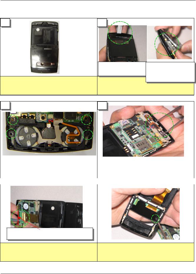
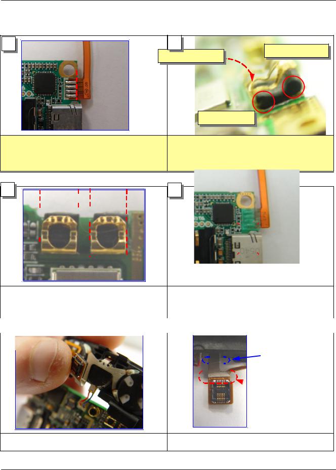
3-3.Disassembling Procedure
1 |
2 |
Open the rear case with Put the disassembly tool
your finger |
on lower end of rear |
case
Remove the 3 screws on rear case & Volume Do not disassemble the phone by compulsion Key
3 |
4 |
|
|
|
|
|
|
Remove the Antenna & Audio part by |
|
|
|
|
|
|
|
|
|
||
|
|
|
|
|
|
tweezer |
|
|
|
|
|
|
|
|
|
|
|
|
|
|
|
|
|
|
|
|
|
Remove the 4 screws on Antenna & Audio |
When remove the Antenna part, make |
||||||
|
|
Parts |
|
|
ensure the Vibrator part carefully |
|||
|
|
|
|
|
|
|
|
|
|
|
|
|
|
|
|
|
|
|
5 |
|
|
6 |
|
|
|
|
|
|
|
|
|
|
|
|
|
|
|
|
|
|
|
|
|
|
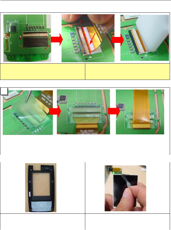
When you remove the FPCB, you must pull up the actuator
Slide up then remove the green tape
Remove the Main PCB and Key pad then remove the 2 screws
3-4
SAMSUNG Proprietary-Contents may change without notice
This Document can not be used without Samsung's authorization
Exploded view and its Part list
|
7 |
|
|
8 |
|
|
|
||||
|
|
|
|
|
|
|
|
|
|
|
|
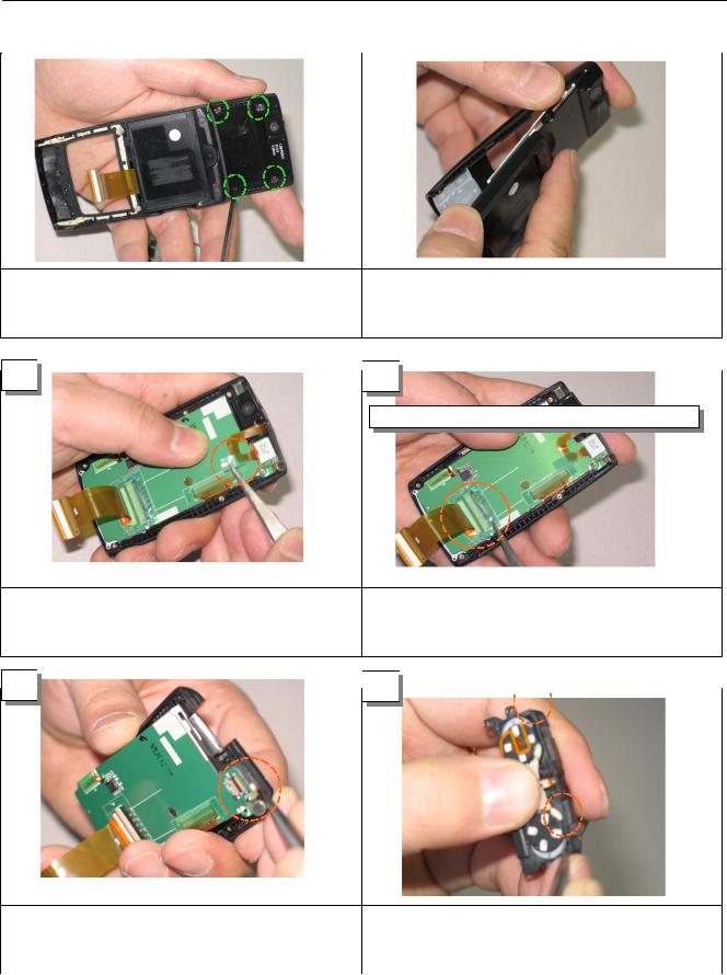
Make a Slide up, then remove the 4 screws |
Disassemble the Slide Part |
|
|
9 
 10
10 

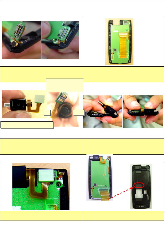
Remove the green tape then remove the FPCB
Before disassemble the Camera part, remove the |
When you remove the FPCB, first pull up the |
green tape |
actuator then removethe FPCB |
|
|
11 
 12
12 

|
Before disassemble the slider PCB, remove |
When you remove the audio part, using a |
|
|
the Receiver part |
removal hole by tweezer |
|
|
|
|
|
|
|
3-5 |
|
|
|
|
|
SAMSUNG Proprietary-Contents may change without notice
This Document can not be used without Samsung's authorization

Exploded view and its Part list
13
When you disassemble the slide part, push the slide part to the upper end
3-6
SAMSUNG Proprietary-Contents may change without notice
This Document can not be used without Samsung's authorization
Exploded view and its Part list
3-4. Assembling Procedure
1 |
2 |
|
|
|
|
|
|
|
|
|
|
|
|
|
|
|
|
|
|
|
|
|
|
|
|
|
|
|
|
|
|
|
|
|
|
|
|
|
|
|
|
|
|
|
|
|
|
|
|
|
|
|
|
|
|
|
|
|
|
|
|
|
|
|
|
|
|
|
|
|
|
|
|
|
|
|
|
|
|
|
|
|
|
|
|
|
|
|
|
|
|
|
|
|
|
|
|
|
|
|
|
|
|
|
|
|
|
|
|
|
|
|
|
|
|
|
|
|
|
|
|
|
|
|
|
|
|
|
|
|
|
|
|
|
|
|
|
|
|
|
|
|
|
|
|
|
|
|
|
|
|
|
|
|
|
|
|
|
|
|
|
|
|
|
|
|
|
|
|
|
|
|
|
|
|
|
|
|
|
|
|
|
|
|
|
|
|
|
|
|
|
|
|
|
|
|
|
|
|
|
|
|
|
|
|
|
|
|
|
|
|
|
|
|
|
|
|
|
|
|
|
|
|
|
|
|
|
|
|
|
|
|
|
|
|
|
|
|
|
|
|
|
|
|
|
|
|
|
|
|
|
|
|
|
|
|
|
|
|
|
|
|
|
|
|
|
|
|
|
|
|
|
|
|
|
|
|
|
|
|
|
|
|
|
|
|
|
|
|
|
|
|
|
|
|
|
|
|
|
|
|
|
|
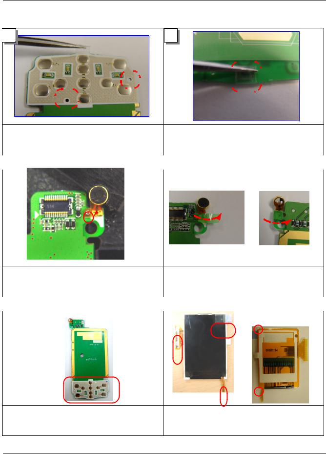
Check the guide holes for |
|
|
The lower part of dome sheet should |
||||||||||||||||||||||||
|
|
|
dome sheet |
|
|
|
be attached on the rear side of PCB |
||||||||||||||||||||||
|
|
|
|
|
|
|
|
|
|
|
|
|
|
|
|
|
|
|
|
|
|
|
|
|
|
|
|
|
|
|
|
|
|
|
|
|
|
|
|
|
|
|
|
|
|
|
|
|
|
|
|
|
|
|
|
|
|
|
|
|
|
|
|
|
|
|
|
|
|
|
|
|
|
|
|
|
|
|
|
|
|
|
|
|
|||||
|
3 |
|
|
|
|
|
|
|
|
|
|
|
|
|
|
4 |
|
|
|
|
|
|
|
|
|
|
|
|
|
|
|
|
|
|
|
|
Soldering |
|
|
|
|
|
|
|
|
|
|
|
|||||||||||
|
|
|
|
|
|
|
|
|
Point |
|
|
|
|
|
|
|
|
|
|
|
|
|
|
|
|
||||
|
|
|
|
|
|
|
|
|
|
|
|
|
|
|
|
|
|
|
|
|
|
|
|
|
|||||
|
|
|
|
|
|
|
|
|
|
|
|
|
|
|
|
|
|
|
|
|
|
|
|
|
|
|
|
|
|
|
|
|
|
|
|
|
|
|
|
|
|
|
|
|
|
|
|
|
|
|
|
|
|
|
|
|
|
|
|
|
|
|
|
|
|
|
|
|
|
|
|
|
|
|
|
|
|
|
|
|
|
|
|
|
|
|
|
|
|
|
|
|
|
|
|
|
|
|
|
|
|
|
|
|
|
|
|
|
|
|
|
|
|
|
|
|
|
|
|
|
Solder the sub_microphone guided by |
Adhere the non-conductive tape on |
||||||
|
|
|
it's soldering point |
|
the soldering point of SUB_MIC |
|||
|
|
|
|
|
|
|
|
|
|
|
|
|
|
|
|
|
|
|
|
|
|
|
|
|
|
|
|
|
5 |
|
|
|
|
6 |
|
|
|
|
|
|
|
|
|
|
|
|
|
|
|
|
|
|
|
|
|
|
|
|
|
|
|
|
|
|
|
|
|
|
|
|
|
.Check the guide hole on right |
Check the Hot Bar, Backlight FPCB, |
position |
Heat seal and Guide poles |
|
|
3-7
SAMSUNG Proprietary-Contents may change without notice
This Document can not be used without Samsung's authorization
Exploded view and its Part list
7 |
8 |
|
|
Check the guide hole on right |
|
Adjust between each corners of LCD |
|||||
|
|
position |
|
module and Guiding edges on PCB |
|||||
|
|
|
|
|
|
|
|
|
|
|
|
|
|
|
|
|
|
|
|
|
|
|
|
|
|
|
GUIDE MARK |
|
|
|
9 |
|
|
10 |
|
|
|
|
|
|
|
|
|
|
|
|
|
||
|
|
|
|
|
|
|
|
|
|
|
|
|
|
|
|
|
|
|
|
|
|
|
|
|
|
|
|
|
|
|
|
|
|
|
|
|
|
|
|
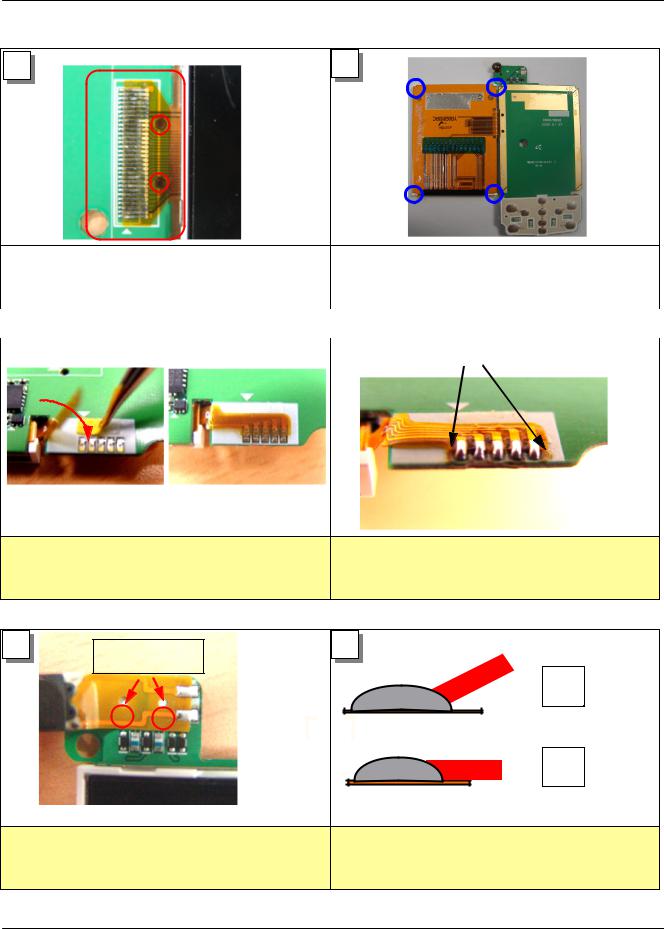
Solder the backlight FPCB
Be careful of two guide marks on soldering process
11 |
Guide hole |
12 |
|
|
|
|
|
NG |
OK
Solder the Receiver on PCB
Receiver's FPCB should be parallel to the PCB
3-8
SAMSUNG Proprietary-Contents may change without notice
This Document can not be used without Samsung's authorization

Exploded view and its Part list
13 |
14 |
|
|
|
|
|
|
|
|
|
|
|
|
|
|
|
|
|
|
|
|
|
|
|
|
|
|
|
|
|
|
|
|
|
|
|
|
|
|
|
|
|
|
|
|
|
|
|
|
|
|
|
|
|
|
|
|
|
|
|
|
|
|
|
|
|
|
|
|
|
|
|
|
|
|
|
|
|
|
|
|
|
|
|
|
|
|
|
|
|
|
|
|
|
|
|
|
|
|
|
|
|
|
|
|
|
|
|
|
|
|
|
|
|
|
|
|
|
|
|
|
|
|
|
|
|
|
|
|
|
|
|
|
|
|
|
|
|
|
|
|
|
|
|
|
|
|
|
|
|
|
|
|
|
|
|
|
|
|
|
|
|
|
|
|
|
|
|
|
|
|
|
|
|
|
|
|
|
|
|
|
|
|
|
|
|
|
|
|
|
|
|
|
|
|
|
|
|
|
|
|
|
|
|
|
|
|
|
|
|
|
|
|
|
|
|
|
|
|
|
|
|
|
|
|
|
|
|
|
|
|
|
|
|
|
|
|
|
|
|
|
|
|
|
|
|
|
|
|
|
|
|
|
|
|
|
|
|
|
|
|
|
|
|
|
|
|
|
|
|
|
|
|
|
|
|
|
|
|
|
|
|
|
|
|
|
|
|
|
|
|
|
|
|
|
|
|
|
|
|
|
|
|
|
|
|
|
|
|
|
|
|
|
|
|
|
|
|
|
|
|
|
|
|
|
|
|
|
|
|
|
|
|
|
|
|
|
|
|
|
|
|
|
|
|
|
|
|
|
|
|
|
|
|
|
|
|
|
|
|
|
|
|
|
|
|
|
|
|
|
|
|
|
|
|
|
|
|
|
|
|
|
|
|
|
|
|
|
|
|
|
|
|
|
|
|
|
|
|
|
|
|
|
|
|
|
|
|
|
|
|
|
|
|
|
|
|
|
|
|
|
|
|
|
|
|
|
|
|
|
|
|
|
|
|
|
|
|
|
|
|
|
|
|
|
|
|
|
|
|
|
|
|
|
|
|
|
|
|
|
|
|
|
|
|
|
|
|
|
|
|
|
|
|
|
|
|
|
|
|
|
|
|
|
|
|
|
|
|
|
|
|
|
|
|
|
|
|
|
|
|
|
|
|
|
|
|
|
|
|
|
|
|
|
|
|
|
|
|
|
|
|
|
|
|
|
|
|
|
|
|
|
|
|
|
|
|
|
|
|
|
|
|
|
|
|
|
|
|
|
|
|
|
|
|
|
|
|
|
|
|
|
|
|
|
|
|
|
|
|
|
|
|
|
|
|
|
|
|
|
|
|
|
|
|
|
|
|
|
|
|
|
|
|
|
|
|
|
|
|
|
|
|
|
|
|
|
|
|
|
|
|
|
|
|
|
|
|
|
|
|
|
|
|
|
|
|
|
|
|
|
|
|
|
|
|
|
|
|
|
|
|
|
|
|
|
|
|
|
|
|
|
|
|
|
|
|
|
|
|
|
|
|
|
|
|
|
|
|
|
|
|
|
|
|
|
|
|
|
|
|
|
|
|
|
|
|
|
|
|
|
|
|
|
|
|
|
|
|
|
|
|
|
|
|
|
|
|
|
|
|
|
|
|
|
|
|
|
|
|
|
|
|
|
|
|
|
|
|
|
|
|
|
|
|
|
|
|
|
|
|
|
|
|
|
|
|
|
|
|
|
|
|
|
|
|
|
|
|
|
|
|
|
|
|
|
|
|
|
|
|
|
|
|
|
|
|
|
|
|
|
|
|
|
|
|
|
|
|
|
|
|
|
|
|
|
|
|
|
|
|
|
|
|
|
|
|
|
|
|
|
|
|
|
|
|
|
|
|
|
|
|
|
|
|
|
|
|
|
|
|
|
|
|
|
|
|
|
|
|
|
|
|
|
|
|
|
|
|
|
|
|
|
|
|
|
|
|
|
|
|
|
|
|
|
|
|
|
|
|
|
|
|
|
|
|
|
|
|
|
|
|
|
|
|
|
|
|
|
|
|
|
|
|
|
|
|
|
|
|
|
|
|
|
|
|
|
|
|
|
|
|
|
|
|
|
|
|
|
|
|
|
|
|
|
|
|
|
|
|
|
|
|
|
|
|
|
|
|
|
|
|
|
|
|
|
Adhere the non-conductive tape on |
|
Adhere the non-conductive tape on |
|||||||||||||||||||||||||||||||||||||||||||||||||||||||
|
|
left side of PCB |
|
|
|
the charger pump |
||||||||||||||||||||||||||||||||||||||||||||||||||||
|
|
|
|
|
|
|
|
|
|
|
|
|
|
|
|
|
|
|
|
|
|
|
|
|
|
|
|
|
|
|
|
|
|
|
|
|
|
|
|
|
|
|
|
|
|
|
|
|
|
|
|
|
|
|
|
|
|
|
|
|
|
|
|
|
|
|
|
|
|
|
|
|
|
|
|
|
|
|
|
|
|
|
|
|
|
|
|
|
|
|
|
|
|
|
|
|
|
|
|
|
|
|
|
|
|
|
|
|
|
|
|
|
|
|
|
|
|
|
15 |
|
|
|
|
|
|
|
|
|
|
|
|
|
|
|
|
|
|
|
|
|
|
|
|
|
|
|
|
|
|
|
|
|
|
16 |
|
|
|
|
|
|
|
|
|
|
|
|
|
|
|
|
|
|
|
|
|
|
|
|
|
|
|
|
|
|
|
|
|
|
|
|
|
|
|
|
|
|
|
|
|
|
|
|
|
|
|
|
|
|
|
|
|
|
|
|
|
|
|
|
|
|
|
|
|
|
|
|
|
|
|
|
|
|
|
|
|
|
|
|
|
|
|
|
|
|
|
|
|
|
|
|
|
|
|
|
|
|
|
|
|
|
|
|
|
|
|
|
|
|
|
|
|
|
|
|
|
|
|
|
|
|
|
|
|
|
|
|
|
|
|
|
|
|
|
|
|
|
|
|
|
|
|
|
|
|
|
|
|
|
|
|
|
|
|
|
|
|
|
|
|
|
|
|
|
|
|
|
|
|
|
|
|
|
|
|
|
|
|
|
|
|
|
|
|
|
|
|
|
|
|
|
|
|
|
|
|
|
|
|
|
|
|
|
|
|
|
|
|
|
|
|
|
|
|
|
|
|
|
|
|
|
|
|
|
|
|
|
|
|
|
|
|
|
|
|
|
|
|
|
|
|
|
|
|
|
|
|
|
|
|
|
|
|
|
|
|
|
|
|
|
|
|
|
|
|
|
|
|
|
|
|
|
|
|
|
|
|
|
|
|
|
|
|
|
|
|
|
|
|
|
|
|
|
|
|
|
|
|
|
|
|
|
|
|
|
|
|
|
|
|
|
|
|
|
|
|
|
|
|
|
|
|
|
|
|
|
|
|
|
|
|
|
|
|
|
|
|
|
|
|
|
|
|
|
|
|
|
|
|
|
|
|
|
|
|
|
|
|
|
|
|
|
|
|
|
|
|
|
|
|
|
Adhere the non-conductive tape on |
Adhere the non-conductive tape on |
Hot-bar |
backlight FPCB |
|
|
|
17 |
|
|
|
|
|
|
|
|
|
18 |
|
|
|
|
|
|
|
|||||||||
|
|
|
|
|
|
|
|
|
|
|
|
|
|
|
|
|
|
|
|
|
|
|
|
|
|
|
|
|
|
|
|
|
|
|
|
|
|
|
|
|
|
|
|
|
|
|
|
|
|
|
|
|
|
|
|
|
|
|
|
|
|
|
|
|
|
|
|
|
|
|
|
|
|
|
|
|
|
|
|
|
|
|
|
|
|
|
|
|
|
|
|
|
|
|
|
|
|
|
|
|
|
|
|
|
|
|
|
|
|
|
|
|
|
|
|
|
|
|
|
|
|
|
|
|
|
|
|
|
|
|
|
|
|
|
|
|
|
|
|
|
|
|
|
|
|
|
|
|
|
|
|
|
|
|
|
|
|
|
|
|
|
|
|
|
|
|
|
Solder and bond the vibrator's wire |
Paste the Bluetooth Ant. on the right |
and bend it on picture's direction |
side Speaker |
|
3-9 |
SAMSUNG Proprietary-Contents may change without notice
This Document can not be used without Samsung's authorization
Exploded view and its Part list
19 |
20 |
Higher side |
|
Push lightly |
|
|
|
|
|
Lower side |
|
Solder the side key FPCB. Adjust the |
|
|
PCB outline and be careful of |
Insert the rubber for intenna contact |
|
electrical shortage. |
|
|
21 |
22 |
|
|
|
|
|
|
|
|
|
|
|
|
|
|
|
|
|
|
|
|
|
|
|
|
|
|
|
|
|
|
|
|
|
|
|
|
|
|
|
|
|
|
|
|
|
|
|
|
|
|
|
|
|
|
|
|
|
|
|
|
|
|
|
|
|
|
|
|
|
|
|
|
|
|
|
|
|
|
|
|
|
|
|
|
|
|
|
|
|
|
|
|
|
|
|
|
|
|
|
|
|
|
|
|
|
|
|
|
|
|
|
|
|
|
|
|
|
|
|
|
|
|
|
|
|
|
|
|
|
|
|
|
|
|
|
|
|
|
|
|
|
|
|
|
|
|
|
|
|
|
|
|
|
|
|
|
|
|
|
|
|
|
|
|
|
|
|
|
|
|
|
|
|
|
|
|
|
|
|
|
|
|
|
|
|
|
|
|
|
|
|
|
|
|
|
|
|
|
|
|
|
|
|
|
|
|
|
|
|
|
|
|
|
|
|
|
|
|
|
|
|
|
|
|
|
|
|
|
|
|
|
|
|
|
|
|
|
|
|
|
|
|
|
|
|
|
|
|
|
|
|
|
|
|
|
|
|
|
|
|
|
|
|
|
|
|
|
|
|
|
|
|
|
|
|
|
|
|
|
|
|
|
|
|
|
|
|
|
|
|
|
|
|
|
|
|
|
|
|
|
|
|
|
|
|
|
|
|
|
|
|
|
|
|
|
|
|
|
|
|
|
|
|
|
|
|
|
|
|
|
|
|
|
|
|
|
|
|
|
|
|
|
|
|
|
|
|
|
|
|
|
|
|
|
|
|
|
|
|
|
|
|
|
|
|
|
|
|
|
|
|
|
|
|
|
|
|
|
|
|
|
|
|
|
|
|
|
|
|
|
|
|
|
|
|
|
|
|
|
|
|
|
|
|
|
|
|
|
|
|
|
|
|
|
|
|
|
|
|
|
|
|
|
|
|
|
|
|
|
|
|
|
|
|
|
|
|
|
|
|
|
|
|
|
|
|
|
|
|
|
|
|
|
|
|
|
|
|
|
|
|
|
|
|
|
|
|
|
|
|
|
|
|
|
|
|
|
|
|
|
|
|
|
|
|
|
|
|
|
|
|
|
|
|
|
|
|
|
|
|
|
|
|
|
|
|
|
|
|
|
|
|
|
|
|
|
|
|
|
|
|
|
|
|
|
|
|
|
|
|
|
|
|
|
|
|
|
|
|
|
|
|
|
|
|
|
|
|
|
|
|
|
|
|
|
|
|
|
|
|
|
|
|
|
|
|
|
|
|
|
|
|
|
|
|
|
|
|
|
|
|
|
|
|
|
|
|
|
|
|
|
|
|
|
|
|
|
|
|
|
|
|
|
|
|
|
|
|
|
|
|
|
|
|
|
|
|
|
|
|
|
|
|
|
|
|
|
|
|
|
|
|
|
|
|
|
|
|
|
|
|
|
|
|
|
|
|
|
|
|
|
|
|
|
|
|
|
|
|
|
|
|
|
|
|
|
|
|
|
|
|
|
|
|
|
|
|
|
|
|
|
|
|
|
|
|
|
|
|
|
|
|
|
|
|
|
|
|
|
|
|
|
|
|
|
|
|
|
|
|
|
|
|
|
|
|
|
|
|
|
|
|
|
|
|
|
|
|
|
|
|
|
|
|
|
|
|
|
|
|
|
|
|
|
|
|
|
|
|
|
|
|
|
|
|
|
|
|
|
|
|
|
|
|
|
|
|
|
|
|
|
|
|
|
|
|
|
|
|
|
|
|
|
|
|
|
|
|
|
|
|
|
|
|
|
|
|
|
|
|
|
|
|
|
|
|
|
|
|
|
|
|
|
|
|
|
|
|
|
|
|
|
|
|
|
|
|
|
|
|
|
|
|
|
|
|
|
|
|
|
|
|
|
|
|
|
|
|
|
|
|
|
|
|
|
|
|
|
|
|
|
|
|
|
|
|
|
|
|
|
|
|
|
|
|
|
|
|
|
|
|
|
|
|
|
|
|
|
|
|
|
|
|
|
|
|
|
|
|
|
|
|
|
|
|
|
|
|
|
|
|
|
|
|
|
|
|
|
|
|
|
|
|
|
|
|
|
|
|
|
|
|
|
|
|
|
|
|
|
|
|
|
|
|
|
|
|
|
|
|
|
|
|
|
|
|
|
|
|
|
|
|
|
|
|
|
|
|
|
|
|
|
|
|
|
|
|
|
|
|
|
|
|
|
|
|
|
|
|
|
|
|
|
|
|
|
|
|
|
|
|
|
|
|
|
|
|
|
|
|
|
|
|
|
|
|
|
|
|
|
|
|
|
|
|
|
|
|
|
|
|
|
|
|
|
|
|
|
|
|
|
|
|
Rubber should be place on aligned |
|
Adhere the non-conductive tape on |
||||||||||||||||||||||||||||||||||||||||||||||||||||||||||||
|
|
|
|
|
|
|
|
|
position on the red line |
|
|
the solder point of side key |
||||||||||||||||||||||||||||||||||||||||||||||||||||
|
|
|
|
|
|
|
|
|
|
|
|
|
|
|
|
|
|
|
|
|
|
|
|
|
|
|
|
|
|
|
|
|
|
|
|
|
|
|
|
|
|
|
|
|
|
|
|
|
|
|
|
|
|
|
|
|
|
|
|
|
|
|
|
|
|
|
|
|
|
|
|
|
|
|
|
|
|
|
|
|
|
|
|
|
|
|
|
|
|
|
|
|
|
|
|
|
|
|
|
|
|
|
|
|
|
|
|
|
|
|
|
|
|
|
|
|
|
|
|
|
|
|
|
|
|
|
|
|
|
|
|
|
|
|
|
|
|
|
|
|
|
|
|
|
|
|
|
|
|
|
|
|
|
|
|
|
|
|
|
|
|
|
|
|
|
|
|
|
|
|
|
|
|
|
|
|
|
|
|
|
|
|
|
|
|
|
|
|
|
|
|
|
Bending point |
|
|
|
23 |
|
|
|
|
|
|
|
|
|
|
|
|
|
|
|
|
|
|
|
|
|
|
|
|
|
|
|
|
|
|
|
|
|
|
|
|
|
|
|
|
|
|
24 |
|
|
|
|
|
|
|
|
|
|
|
|
|
|
|
|
|
||
|
|
|
|
|
|
|
|
|
|
|
|
|
|
|
|
|
|
|
|
|
|
|
|
|
|
|
|
|
|
|
|
|
|
|
|
|
|
|
|
|
|
|
|
|
|
|
|
|
|
|
|
|
|
|
|
|
|
|
|
|
|
|
of FPCB |
(the |
|
|
|
|
|
|
|
|
|
|
|
|
|
|
|
|
|
|
|
|
|
|
|
|
|
|
|
|
|
|
|
|
|
|
|
|
|
|
|
|
|
|
|
|
|
|
|
|
|
|
|
|
|
|
|
|
|
|
|
|
|
|
|
||
|
|
|
|
|
|
|
|
|
|
|
|
|
|
|
|
|
|
|
|
|
|
|
|
|
|
|
|
|
|
|
|
|
|
|
|
|
|
|
|
|
|
|
|
|
|
|
|
|
|
|
|
|
|
|
|
|
|
|
|
|
|
|
||
|
|
|
|
|
|
|
|
|
|
|
|
|
|
|
|
|
|
|
|
|
|
|
|
|
|
|
|
|
|
|
|
|
|
|
|
|
|
|
|
|
|
|
|
|
|
|
|
|
|
|
|
|
|
|
|
|
|
|
|
|
|
|
||
|
|
|
|
|
|
|
|
|
|
|
|
|
|
|
|
|
|
|
|
|
|
|
|
|
|
|
|
|
|
|
|
|
|
|
|
|
|
|
|
|
|
|
|
|
|
|
|
|
|
|
|
|
|
|
|
|
|
|
|
|
|
|
form of |
'U') |
|
|
|
|
|
|
|
|
|
|
|
|
|
|
|
|
|
|
|
|
|
|
|
|
|
|
|
|
|
|
|
|
|
|
|
|
|
|
|
|
|
|
|
|
|
|
|
|
|
|
|
|
|
|
|
|
|
|
|
|
|
|
|
||
|
|
|
|
|
|
|
|
|
|
|
|
|
|
|
|
|
|
|
|
|
|
|
|
|
|
|
|
|
|
|
|
|
|
|
|
|
|
|
|
|
|
|
|
|
|
|
|
|
|
|
|
|
|
|
|
|
|
|
|
|
|
|
||
 This point should not be bended
Bend the SPK FPCB |
The bending point of SPK FPCB |
|
|
3-10
SAMSUNG Proprietary-Contents may change without notice
This Document can not be used without Samsung's authorization
Exploded view and its Part list
|
25 |
|
|
|
|
|
|
|
|
|
|
|
|
|
|
|
|
|
|
|
|
|
|
|
|
|
|
|
|
|
|
|
|
|
|
|
|
|
|
|
|
|
|
|
|
|
|
|
|
|
|
|
|
|
|
|
|
|
|
|
|
|
|
|
|
|
|
|
|
|
|
|
|
|
|
|
|
|
|
|
|
|
|
|
|
|
|
|
|
|
|
|
|
|
|
|
|
|
|
|
|
|
|
|
|
|
|
|
Check the white |
|
Push & Paste |
|||||
|
|
|
|
|
|
|
|
|
|
|
|
|
|
|
|
|
|
|
|
|
|
|
|
|
|
|
|
|
|
|
|
|
|
|
||||
|
|
|
|
|
|
|
|
|
|
|
|
|
|
|
|
|
|
|
|
|
|
|
|
|
|
|
|
|
|
|
|
|
|
|
||||
|
|
|
|
|
|
|
|
|
|
|
|
|
|
|
|
|
|
|
|
|
|
|
|
|
|
|
|
|
|
|
|
|
|
silk line |
|
|
||
|
|
|
|
|
|
|
|
|
|
|
|
|
|
|
|
|
|
|
|
|
|
|
|
|
|
|
|
|
|
|
|
|
|
|
|
|||
|
|
|
|
|
|
|
|
|
|
|
|
|
|
|
|
|
|
|
|
|
|
|
|
|
|
|
|
|
|
|
|
|
|
|
|
|
|
|
|
|
|
|
|
|
|
|
|
|
|
|
|
|
|
|
|
|
|
|
|
|
|
|
|
|
|
|
|
|
|
|
|
|
|
|
|
|
|
|
|
|
|
|
|
|
|
|
|
|
|
|
|
|
|
|
|
|
|
|
|
|
|
|
|
|
|
|
|
|
|
|
|
|
|
|
|
|
|
|
|
|
|
|
|
|
|
|
|
|
|
|
|
|
|
|
|
|
|
|
|
|
|
|
|
|
|
|
|
|
|
|
|
|
|
|
|
|
|
|
|
|
|
|
|
|
|
|
|
|
|
|
|
|
|
|
|
|
|
|
|
|
|
|
|
|
|
|
|
|
|
|
|
|
|
|
|
|
|
|
|
|
|
|
|
|
|
|
|
|
|
|
|
|
|
|
|
|
|
|
|
|
|
|
|
|
|
|
|
|
|
|
|
|
|
|
|
|
|
|
|
|
|
|
|
|
|
|
|
|
|
|
|
|
|
|
|
|
|
|
|
|
|
|
|
|
|
|
|
|
|
|
|
|
Remove the protection cover
Check the alignment between FPCB and white silk line
26
|
|
Adhere the non-conductive tape on |
|
Check the alignment between FPCB |
||
|
|
|
FPCB connector of Sub PCB |
|
|
and white silk line |
|
|
|
|
|
|
|
|
|
|
|
|
|
|
|
|
27 |
|
|
28 |
|
|
|
|
|
|
|
|
|
|
|
|
|
|
|
|
Put the Sub Key Pad on the slide |
Remove the protection tape on LCD |
|
|
upper case |
window |
|
|
|
|
|
|
|
3-11 |
|
|
|
|
|
SAMSUNG Proprietary-Contents may change without notice
This Document can not be used without Samsung's authorization
Exploded view and its Part list
|
|
|
|
|
30 |
|
|
|
29 |
|
|
|
|
|
|
|
|
|
|
|
Insert the receiver and Sub MIC into |
Put the sub PBA assy. on the slide |
|||||||
each holder on the slide upper case |
|
upper case |
||||||
|
|
|
|
|
from '2' to '1' |
|
|
|
|
|
|
|
|
|
|
||
|
|
|
|
|
direction |
|
|
|
|
31 |
|
|
|
|
|
32 |
|
|
|
|
|
|||||
|
|
|
|
|
|
|
|
|
|
|
|
|
|
|
|
|
|
|
|
|
|
|
|
|
|
|
1 2
Wind the FPCB twice
Wind the camera's FPCB on the its
Insert the camera module on the
hinge
fron case
(put on the camera's hinge first)
|
|
|
|
|
|
|
34 |
|
|
|
|
|
33 |
|
|
|
|
|
|
|
|
|
|
|
|
|
|
|
|
|
|
|
|
|
|
|
|
|
|
|
|
|
|
|
|
|
|
|
|
|
|
|
|
|
|
|
|
|
|
|
|
|
|
|
|
Adhere the non-conductive tape on |
Pull out the Main FPCB through the |
the cameras FPCB |
slider case's hole(red circle) |
|
3-12 |
SAMSUNG Proprietary-Contents may change without notice
This Document can not be used without Samsung's authorization
Exploded view and its Part list
|
|
|
|
|
36 |
|
|
|
35 |
|
|
|
|
|
|
|
|
|
|
|
|
|
|
|
|
|
|
Push the slide lower to the slide |
If there is no problems until now, |
upper's direction |
the current state will be like this |
|
|
37 |
|
38 |
|
SCREW |
SCREW |
|
HOLE |
|
|
HOLE |
|
|
|
Screw down the upper's 4 points |
Screw down the lower's 2 points |
|
|
39
Insert the screw cap |
Be careful of each direction |
|
|
3-13
SAMSUNG Proprietary-Contents may change without notice
This Document can not be used without Samsung's authorization
Exploded view and its Part list
|
|
|
|
|
|
|
|
shield can's |
|
|
|
|
|
|
|
|
|
|
|
|
|
|
MAIN KEY PAD's GUIDE HOLE |
|
|
41 |
|
|
|
|
|
40 |
|
|
|
guide line |
|
||
|
|
|
|
|
|
|
|
|
|
|
|
|
|
|
|
|
|
|
|
|
|
|
|
|
|
|
|
|
|
|
|
|
|
|
|
|
Put the main key pad on the front |
|
Place the shield can over the main |
||
|
|
case |
|
|
key pad |
|
|
|
|
|
|
|
|
|
|
|
|
|
42 |
|
|
43 |
|
|
|
|
|
|
|
|
|
|
|
|
|
|
|
Confirm the |
|
|
|
|
|
||
|
|
alignment |
|
|
|
|
|
|
|
|
|
|
|
|
Confirm the bending state of Main |
Push the main FPCB into the Main |
|||
FPCB |
connector |
|||
|
|
|
|
|
44 |
Push the whole parts |
45 |
|
|
|
|
of FPCB equaly |
Push the middle of actuator |
|||||
|
|
|||||
|
|
|
first and the both sides later |
|||
|
|
|
2 |
1 |
2 |
|
|
Insertion guide |
|
Insertion guide II ; |
|||
|
|
3-14 |
|
|
|
|
SAMSUNG Proprietary-Contents may change without notice
This Document can not be used without Samsung's authorization
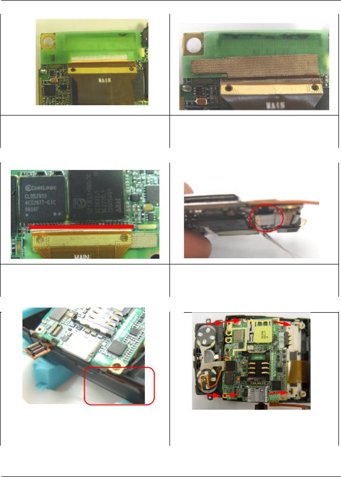
Exploded view and its Part list
|
|
|
|
|
47 |
|
|
|
46 |
|
|
|
|
|
|
|
|
|
|
|
|
|
|
|
|
|
|
|
Adhere the non-conductive tape on |
Adhere the gold gasket over the non- |
|||
|
|
the Main connector of Main PCB |
|
|
conductive tape |
|
|
|
|
|
|
|
|
|
|
|
|
|
48 |
|
|
49 |
|
|
|
|
|
|
|
|
|
|
|
|
|
|
|
Bending line should be aligned with |
|
If the other point is bent, the critical |
|||
|
|
|
the red line |
|
|
display error will be occurred |
|
|
|
|
|
|
|
|
|
|
|
|
|
|
|
|
|
|
|
50 |
|
|
51 |
||
|
|
|
|
|
|
||
|
|
|
|
|
|
|
|
|
|
|
|
|
|
|
|
|
|
|
|
|
|
Bend and push the side key FPCB |
Put the Main PCB on the shield can |
|
into the front case |
in the order described above |
|
|
|
|
3-15
SAMSUNG Proprietary-Contents may change without notice
This Document can not be used without Samsung's authorization
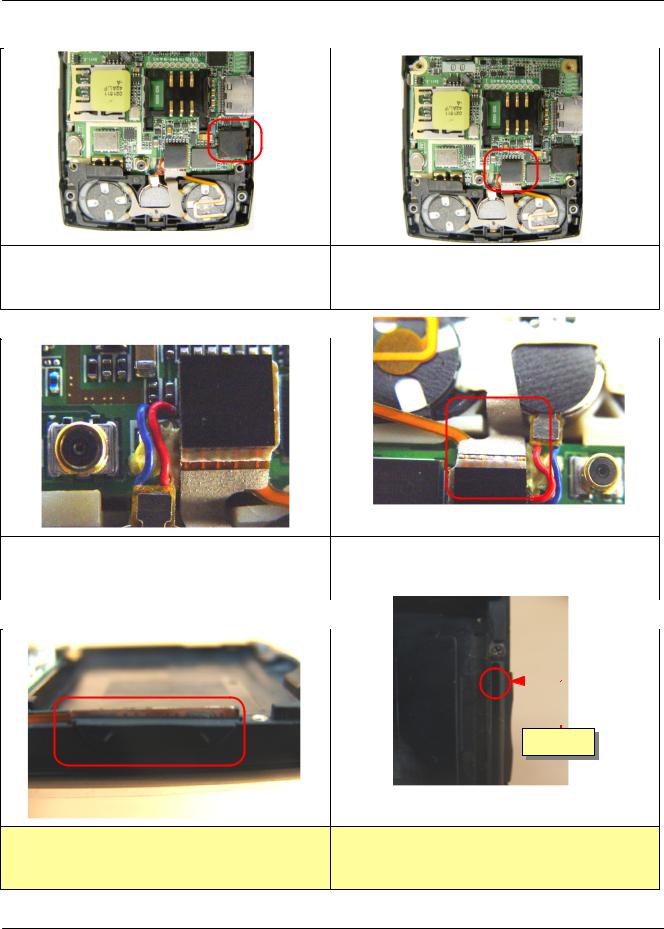
Exploded view and its Part list
|
|
|
|
53 |
|
|
52 |
|
|
|
|
|
|
|
|
|
|
Insert the shield can's connector |
Insert the Speaker's connector |
|
|
|
54 |
|
|
|
|
|
|
|
|
|
|
|
|
|
55 |
|
|
|
|
|
|
|
|
|
|
|
|
|
|
|
|
Reference position of the vibrator's |
Bend as the form of 'U' and push the |
|||||
|
|
|
wire |
|
SPK's FPCB into the inner space |
|||
|
|
|
|
|
|
|
|
|
|
|
|
|
|
|
|
|
|
|
|
56 |
|
|
57 |
|
|
|
|
|
|
|
|
|
|
|
|
|
|
|
|
|
|
|
|
|
|
|
|
|
|
|
|
|
|
SCREW
The picture of side key FPCB on
Screw down the side key's holder
normal condition
3-16
SAMSUNG Proprietary-Contents may change without notice
This Document can not be used without Samsung's authorization

Exploded view and its Part list
|
|
|
|
59 |
|
|
58 |
|
|
|
|
|
|
|
|
|
|
|
|
|
|
|
|
Screw down on each 4 points of
Two red circles' point should be
intenna module
inserted first at the rear case assembly procedure
|
60 |
|
|
|
|
|
|
|
|
|
|
|
|
|
|
|
|
|
61 |
|
|
|
|
|
||||||||
|
|
|
|
|
|
|
|
|
|
|
|
|
|
|
|
|
|
|
|
|
|
|
|
|
|
|
|
|
|
|
|
|
|
|
|
|
|
|
|
|
|
|
|
|
|
|
|
|
|
|
|
|
|
|
|
|
|
|
|
|
|
|
|
|
|
|
|
|
|
|
|
|
|
|
|
|
SCREW
Push each 5 points sufficiently |
Screw down on the last 2 points |
|
|
3-17
SAMSUNG Proprietary-Contents may change without notice
This Document can not be used without Samsung's authorization
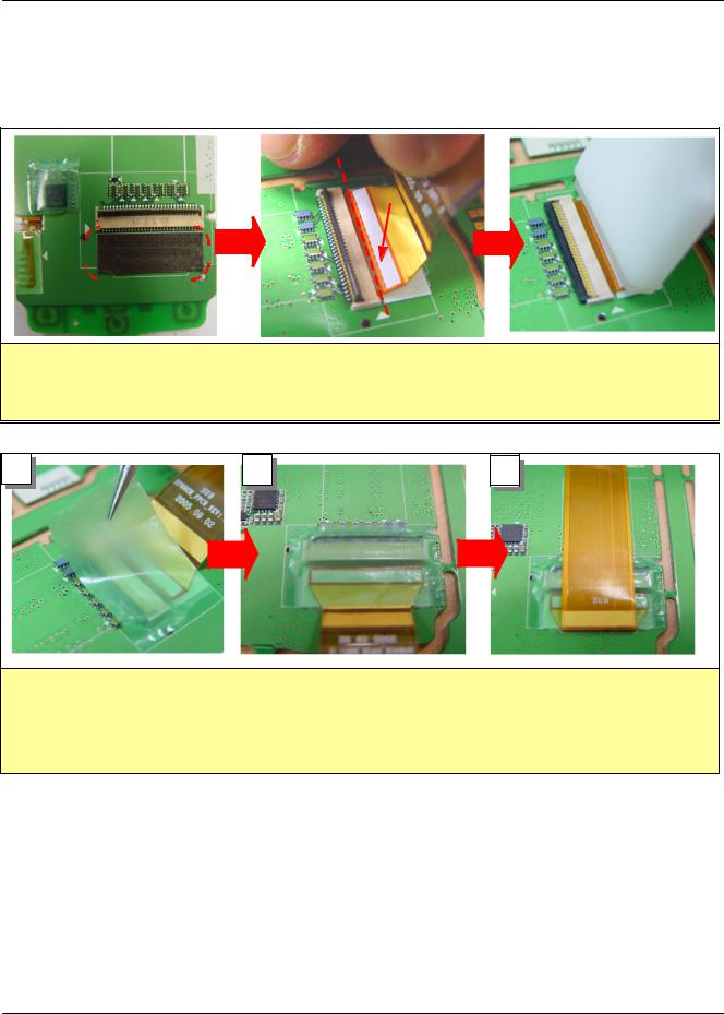
Exploded view and its Part list
3-5. Slide FPCB KIT Assembling Procedure
- Sub PCB Part
|
1 |
|
|
|
|
|
|
|
|
|
|
|
|
|
|
|
|
|
|
|
|
|
|
|
|
|
|
|
|
|
|
|
|
|
2 |
|
|
|
3 |
|
|
|
|
|
|
|
|
|
|
|
|
|
|
|
|
|
|
|
|
|
|
|
|
|
|
|
|
|
|
|
|
|
|
|
|
|
Check the white |
|
|
|
|||||||
|
|
|
|
|
|
|
|
|
|
|
|
|
|
|
|
|
|
|
|
|
|
|
|
|
|
|
|
|
|
|
|
Push & Paste |
|||||||||||
|
|
|
|
|
|
|
|
|
|
|
|
|
|
|
|
|
|
|
|
|
|
|
|
|
|
|
|
|
|
|
|
|
|
|
|
|
|
|
|
|
|
|
|
|
|
|
|
|
|
|
|
|
|
|
|
|
|
|
|
|
|
|
|
|
|
|
|
|
|
|
|
|
|
|
|
|
|
|
|
|
silk line |
|
|
|
|
||
|
|
|
|
|
|
|
|
|
|
|
|
|
|
|
|
|
|
|
|
|
|
|
|
|
|
|
|
|
|
|
|
|
|
|
|
|
|
|
|
|
|||
|
|
|
|
|
|
|
|
|
|
|
|
|
|
|
|
|
|
|
|
|
|
|
|
|
|
|
|
|
|
|
|
|
|
|
|
|
|
|
|
|
|
||
|
|
|
|
|
|
|
|
|
|
|
|
|
|
|
|
|
|
|
|
|
|
|
|
|
|
|
|
|
|
|
|
|
|
|
|
|
|
|
|
|
|
|
|
|
|
|
|
|
|
|
|
|
|
|
|
|
|
|
|
|
|
|
|
|
|
|
|
|
|
|
|
|
|
|
|
|
|
|
|
|
|
|
|
|
|
|
|
|
|
|
|
|
|
|
|
|
|
|
|
|
|
|
|
|
|
|
|
|
|
|
|
|
|
|
|
|
|
|
|
|
|
|
|
|
|
|
|
|
|
|
|
|
|
|
|
|
|
|
|
|
|
|
|
|
|
|
|
|
|
|
|
|
|
|
|
|
|
|
|
|
|
|
|
|
|
|
|
|
|
|
|
|
|
|
|
|
|
|
|
|
|
|
|
|
|
|
|
|
|
|
|
|
|
|
|
|
|
|
|
|
|
|
|
|
|
|
|
|
|
|
|
|
|
|
|
|
|
|
|
|
|
|
|
|
|
|
|
|
|
|
|
|
|
|
|
|
|
|
|
|
|
|
|
|
|
|
|
|
|
|
|
|
|
|
|
|
|
|
|
|
|
|
|
|
|
|
|
|
|
|
|
|
|
|
|
|
|
|
|
|
|
|
|
|
|
|
|
|
|
|
|
|
|
|
|
|
|
|
|
|
|
|
|
|
|
|
|
1.Check the condition of FPCB and remove the protection cover of Sub PCB
2.Check the alignment between FPCB and white silk line
3.Push and Paste evenly by pushing tool
4 |
5 |
6 |
4.Adhere the non-conductive tape on FPCB connector of Sub PCB
5.Check the condition of attachment
6.Bend the FPCB upward and check the alignment between FPCB and white silk line
3-18
SAMSUNG Proprietary-Contents may change without notice
This Document can not be used without Samsung's authorization
Loading...