

Page 1

Compact™ 8-Bit Low Resolution Analog I/O Combination Module
(Catalog Number 1769-IF4XOF2)
User Manual
Page 2
Important User Information
Because of the variety of uses for the products described in this
publication, those responsible for the application and use of this
control equipment must satisfy themselves that all necessary steps
have been taken to assure that each application and use meets all
performance and safety requirements, including any applicable laws,
regulations, codes and standards.
The illustrations, charts, sample programs and layout examples shown
in this guide are intended solely for purposes of example. Since there
are many variables and requirements associated with any particular
installation, Allen-Bradley does not assume responsibility or liability
(to include intellectual property liability) for actual use based upon
the examples shown in this publication.
Allen-Bradley publication SGI-1.1, Safety Guidelines for the
Application, Installation and Maintenance of Solid-State Control
(available from your local Allen-Bradley office), describes some
important differences between solid-state equipment and
electromechanical devices that should be taken into consideration
when applying products such as those described in this publication.
Reproduction of the contents of this copyrighted publication, in whole
or part, without written permission of Rockwell Automation, is
prohibited.
Throughout this manual we use notes to make you aware of safety
considerations:
ATTENTION
Identifies information about practices or
circumstances that can lead to personal injury or
death, property damage or economic loss
!
Attention statements help you to:
• identify a hazard
• avoid a hazard
• recognize the consequences
IMPORTANT
MicroLogix, Compact, RSLogix and RSLinx are trademarks of Rockwell Automation.
Belden is a trademark of Belden, Inc.
DeviceNet is a trademark of Open DeviceNet Vendor Association (ODVA).
Identifies information that is critical for successful
application and understanding of the product.
Page 3

Overview
Table of Contents
Preface
Who Should Use This Manual . . . . . . . . . . . . . . . . . . . . . . P-1
How to Use This Manual. . . . . . . . . . . . . . . . . . . . . . . . . . P-1
Manual Contents . . . . . . . . . . . . . . . . . . . . . . . . . . . . . P-1
Related Documentation . . . . . . . . . . . . . . . . . . . . . . . . . . . P-2
Conventions Used in This Manual . . . . . . . . . . . . . . . . . . . P-2
Rockwell Automation Support . . . . . . . . . . . . . . . . . . . . . . P-3
Local Product Support . . . . . . . . . . . . . . . . . . . . . . . . . P-3
Technical Product Assistance . . . . . . . . . . . . . . . . . . . . P-3
Your Questions or Comments on the Manual . . . . . . . . P-3
Chapter 1
How to Use Analog I/O . . . . . . . . . . . . . . . . . . . . . . . . . . 1-1
General Description of the Module’s Hardware
and Diagnostic Features . . . . . . . . . . . . . . . . . . . . . . . . . . 1-2
Hardware Features. . . . . . . . . . . . . . . . . . . . . . . . . . . . 1-2
General Diagnostic Features . . . . . . . . . . . . . . . . . . . . . 1-4
Overview of the Analog System. . . . . . . . . . . . . . . . . . . . . 1-4
System Operation . . . . . . . . . . . . . . . . . . . . . . . . . . . . 1-5
Module Operation . . . . . . . . . . . . . . . . . . . . . . . . . . . . 1-6
Module Calibration . . . . . . . . . . . . . . . . . . . . . . . . . . . 1-6
Quick Start for Experienced Users
Installation and Wiring
Chapter 2
Before You Begin . . . . . . . . . . . . . . . . . . . . . . . . . . . . . . . 2-1
Required Tools and Equipment . . . . . . . . . . . . . . . . . . . . . 2-1
What You Need To Do . . . . . . . . . . . . . . . . . . . . . . . . . . . 2-2
Chapter 3
Compliance to European Union Directives . . . . . . . . . . . . . 3-1
EMC Directive . . . . . . . . . . . . . . . . . . . . . . . . . . . . . . . 3-1
Low Voltage Directive . . . . . . . . . . . . . . . . . . . . . . . . . 3-2
Power Requirements . . . . . . . . . . . . . . . . . . . . . . . . . . . . . 3-2
General Considerations to Avoid Electrostatic Damage . . . . 3-2
Hazardous Location Considerations . . . . . . . . . . . . . . . 3-3
Prevent Electrostatic Discharge . . . . . . . . . . . . . . . . . . . 3-3
Remove Power . . . . . . . . . . . . . . . . . . . . . . . . . . . . . . 3-4
Reducing Electrical Noise Interference . . . . . . . . . . . . . 3-4
Protecting the Circuit Board from Contamination. . . . . . 3-5
System Assembly. . . . . . . . . . . . . . . . . . . . . . . . . . . . . . . . 3-5
Mounting the Module . . . . . . . . . . . . . . . . . . . . . . . . . . . . 3-6
Minimum Spacing . . . . . . . . . . . . . . . . . . . . . . . . . . . . 3-7
Panel Mounting . . . . . . . . . . . . . . . . . . . . . . . . . . . . . . 3-7
DIN Rail Mounting. . . . . . . . . . . . . . . . . . . . . . . . . . . . 3-8
Replacing a Single Module within a System . . . . . . . . . . . . 3-9
i Publication 1769-UM008A-EN-P - November 2001
Page 4

Table of Contents ii
1769-IF4XOF2 Module Data, Status,
and Configuration Channels
Field Wiring Connections . . . . . . . . . . . . . . . . . . . . . . . . . 3-10
Grounding. . . . . . . . . . . . . . . . . . . . . . . . . . . . . . . . . . 3-10
System Wiring Guidelines. . . . . . . . . . . . . . . . . . . . . . . 3-10
Removing the Finger-Safe Terminal Block. . . . . . . . . . . 3-14
Wiring the Finger-Safe Terminal Block . . . . . . . . . . . . . 3-15
Analog Input Wiring . . . . . . . . . . . . . . . . . . . . . . . . . . . . 3-16
Terminal Door Label . . . . . . . . . . . . . . . . . . . . . . . . . . 3-18
Analog Output Wiring . . . . . . . . . . . . . . . . . . . . . . . . . . . 3-21
Chapter 4
Module Addressing . . . . . . . . . . . . . . . . . . . . . . . . . . . . . . 4-1
Input/Output/Configuration Data Registers . . . . . . . . . . 4-2
Input Data File. . . . . . . . . . . . . . . . . . . . . . . . . . . . . . . . . 4-3
Input Image. . . . . . . . . . . . . . . . . . . . . . . . . . . . . . . . . 4-3
Input Data Words 0 through 3 . . . . . . . . . . . . . . . . . . . 4-4
Input Data Words 4 through 7 . . . . . . . . . . . . . . . . . . . 4-4
Bit Definitions for Input Data . . . . . . . . . . . . . . . . . . . . 4-4
Input Data Resolution and Format . . . . . . . . . . . . . . . . 4-6
Output Data File . . . . . . . . . . . . . . . . . . . . . . . . . . . . . . . . 4-7
Output Data Words 0 and 1 . . . . . . . . . . . . . . . . . . . . . 4-7
Output Data Resolution and Format . . . . . . . . . . . . . . . 4-8
Configuration Data File . . . . . . . . . . . . . . . . . . . . . . . . . . . 4-8
Bit Definitions for Configuration Data . . . . . . . . . . . . . . 4-9
Input Filter Selection . . . . . . . . . . . . . . . . . . . . . . . . . . 4-12
Module Diagnostics and
Troubleshooting
Chapter 5
Safety Considerations When Troubleshooting. . . . . . . . . . . 5-1
Indicator Lights . . . . . . . . . . . . . . . . . . . . . . . . . . . . . . 5-1
Activating Devices When Troubleshooting . . . . . . . . . . 5-1
Stand Clear of the Machine. . . . . . . . . . . . . . . . . . . . . . 5-2
Program Alteration. . . . . . . . . . . . . . . . . . . . . . . . . . . . 5-2
Safety Circuits . . . . . . . . . . . . . . . . . . . . . . . . . . . . . . . 5-2
Module Operation vs. Channel Operation . . . . . . . . . . . . . 5-2
Power-up Diagnostics . . . . . . . . . . . . . . . . . . . . . . . . . . . . 5-3
Channel Diagnostics . . . . . . . . . . . . . . . . . . . . . . . . . . . . . 5-3
Out-of-Range Detection . . . . . . . . . . . . . . . . . . . . . . . . 5-3
Critical vs. Non-Critical Errors . . . . . . . . . . . . . . . . . . . . . . 5-4
I/O Module Errors . . . . . . . . . . . . . . . . . . . . . . . . . . . . 5-4
Extended Error Codes . . . . . . . . . . . . . . . . . . . . . . . . . 5-5
Module Condition Errors . . . . . . . . . . . . . . . . . . . . . . . . . . 5-6
Common Hardware Errors . . . . . . . . . . . . . . . . . . . . . . 5-6
Hardware Specific Errors . . . . . . . . . . . . . . . . . . . . . . . 5-6
Module Inhibit Function . . . . . . . . . . . . . . . . . . . . . . . . . . 5-6
Contacting Rockwell Automation . . . . . . . . . . . . . . . . . . . . 5-7
Publication 1769-UM008A-EN-P - November 2001
Page 5

Specifications
Module Addressing and
Configuration with MicroLogix
1500
Configuration Using the
1769-IF4XOF2 Combination Analog
Module with a CompactLogix
System
Table of Contents iii
Appendix A
General Specifications . . . . . . . . . . . . . . . . . . . . . . . . . . . . A-1
Input Specifications. . . . . . . . . . . . . . . . . . . . . . . . . . . . . . A-2
Output Specifications . . . . . . . . . . . . . . . . . . . . . . . . . . . . A-3
Appendix B
Module Addressing . . . . . . . . . . . . . . . . . . . . . . . . . . . . . . B-1
1769-IF4XOF2 Input Image. . . . . . . . . . . . . . . . . . . . . . B-2
1769-IF4XOF2 Configuration File . . . . . . . . . . . . . . . . . B-3
Configuring 1769-IF4XOF2 in a MicroLogix 1500 System. . . B-3
Configuring the 1769-IF4XOF2 . . . . . . . . . . . . . . . . . . . B-6
Appendix C
Adding a 1769-IF4XOF2 Module to Your System . . . . . . . . C-1
Thin Profile . . . . . . . . . . . . . . . . . . . . . . . . . . . . . . . . . C-3
Generic Profile. . . . . . . . . . . . . . . . . . . . . . . . . . . . . . . C-4
Configuring the 1769-IF4XOF2 Analog
Combination Module. . . . . . . . . . . . . . . . . . . . . . . . . . . . . C-5
Accessing the Input and Output Tags. . . . . . . . . . . . . . . . . C-9
Thin Profile . . . . . . . . . . . . . . . . . . . . . . . . . . . . . . . . . C-9
Generic Profile. . . . . . . . . . . . . . . . . . . . . . . . . . . . . . . C-9
Two’s Complement Binary
Numbers
Appendix D
Positive Decimal Values . . . . . . . . . . . . . . . . . . . . . . . . . . D-1
Glossary
Index
Publication 1769-UM008A-EN-P - November 2001
Page 6

Table of Contents iv
Publication 1769-UM008A-EN-P - November 2001
Page 7

Preface
Read this preface to familiarize yourself with the rest of the manual.
This preface covers the following topics:
• Who Should Use This Manual on page P-1
• How to Use This Manual on page P-1
• Related Documentation on page P-2
• Conventions Used in This Manual on page P-2
• Rockwell Automation Support on page P-3
Who Should Use This
Manual
How to Use This Manual
Use this manual if you are responsible for designing, installing,
programming, or troubleshooting control systems that use
Allen-Bradley Compact™ I/O.
As much as possible, we organized this manual to explain, in a
task-by-task manner, how to install, configure, program, operate and
troubleshoot a control system using the analog I/O modules.
Manual Contents
If you want... See
An overview of the analog combination module Chapter 1
A quick start guide for experienced users Chapter 2
Installation and wiring guidelines Chapter 3
Module addressing, configuration and status information Chapter 4
Information on module diagnostics and troubleshooting Chapter 5
Specifications for the combination module Appendix A
Information on addressing and configuration using MicroLogix 1500
and RSLogix 500
Information on configuring the module using CompactLogix and
RSLogix 5000
Information on understanding two’s complement binary numbers Appendix D
Definitions of terms used in this manual Glossary
1 Publication 1769-UM008A-EN-P - November 2001
Appendix B
Appendix C
Page 8

P-2
Related Documentation
The table below provides a listing of publications that contain
important information about MicroLogix 1500 systems.
For Read this document Document number
A user manual containing information on how to install,
use and program your MicroLogix 1500 controller.
A user manual containing information on how to install,
and use your 1769-ADN DeviceNet Adapter.
A user manual containing information on how to install,
use and program your CompactLogix controller.
An overview of 1769 Compact Discrete I/O modules 1769 Compact Discrete Input/Output Modules Product
An overview of the MicroLogix 1500 System, including
1769 Compact I/O.
In-depth information on grounding and wiring
Allen-Bradley programmable controllers.
MicroLogix™ 1500 User Manual 1764-UM001A-US-P
DeviceNet Adapter User Manual 1769-UM001A-US-P
CompactLogix User Manual 1769-UM007C-EN-P
1769-2.1
Data
MicroLogix™ 1500 System Overview 1764-SO001B-EN-P
Allen-Bradley Programmable Controller Grounding and
Wiring Guidelines
1770-4.1
If you would like a manual, you can:
• download a free electronic version from the internet at
www.theautomationbookstore.com
• purchase a printed manual by:
– contacting your local distributor or Rockwell Automation
representative
– visiting www.theautomationbookstore.com and placing
your order
– calling 1.800.963.9548 (USA/Canada) or 001.330.725.1574
(Outside USA/Canada)
Conventions Used in This
Manual
Publication 1769-UM008A-EN-P - November 2001
The following conventions are used throughout this manual:
• Bulleted lists (like this one) provide information not procedural
steps.
• Numbered lists provide sequential steps or hierarchical
information.
• Italic type is used for emphasis.
• Text in this font indicates words or phrases you should type.
Page 9

P-3
Rockwell Automation
Support
Rockwell Automation offers support services worldwide, with over
75 Sales/Support Offices, 512 authorized distributors and 260
authorized Systems Integrators located throughout the United States
alone, plus Rockwell Automation representatives in every major
country in the world.
Local Product Support
Contact your local Rockwell Automation representative for:
• sales and order support
• product technical training
• warranty support
• support service agreement
Technical Product Assistance
If you need to contact Rockwell Automation for technical assistance,
please review the information in Chapter 5, Module Diagnostics and
Troubleshooting first. Then call your local Rockwell Automation
representative.
Your Questions or Comments on the Manual
If you find a problem with this manual, please notify us. If you have
any suggestions for how this manual could be made more useful to
you, please contact us at the address below:
Rockwell Automation
Automation Control and Information Group
Technical Communication, Dept. A602V
P.O. Box 2086
Milwaukee, WI 53201-2086
Publication 1769-UM008A-EN-P - November 2001
Page 10

P-4
Publication 1769-UM008A-EN-P - November 2001
Page 11
Chapter
Overview
This chapter explains how analog data is used and describes the
1769-IF4XOF2 combination analog I/O module. Included is
information about:
• How to Use Analog I/O on page 1-1
• General Description of the Module’s Hardware and Diagnostic
Features on page 1-2
• Overview of the Analog System on page 1-4
1
How to Use Analog I/O
Analog refers to the representation of numerical quantities by the
measurement of continuous physical variables. Analog applications
are present in many forms. The following application shows a typical
use of analog data.
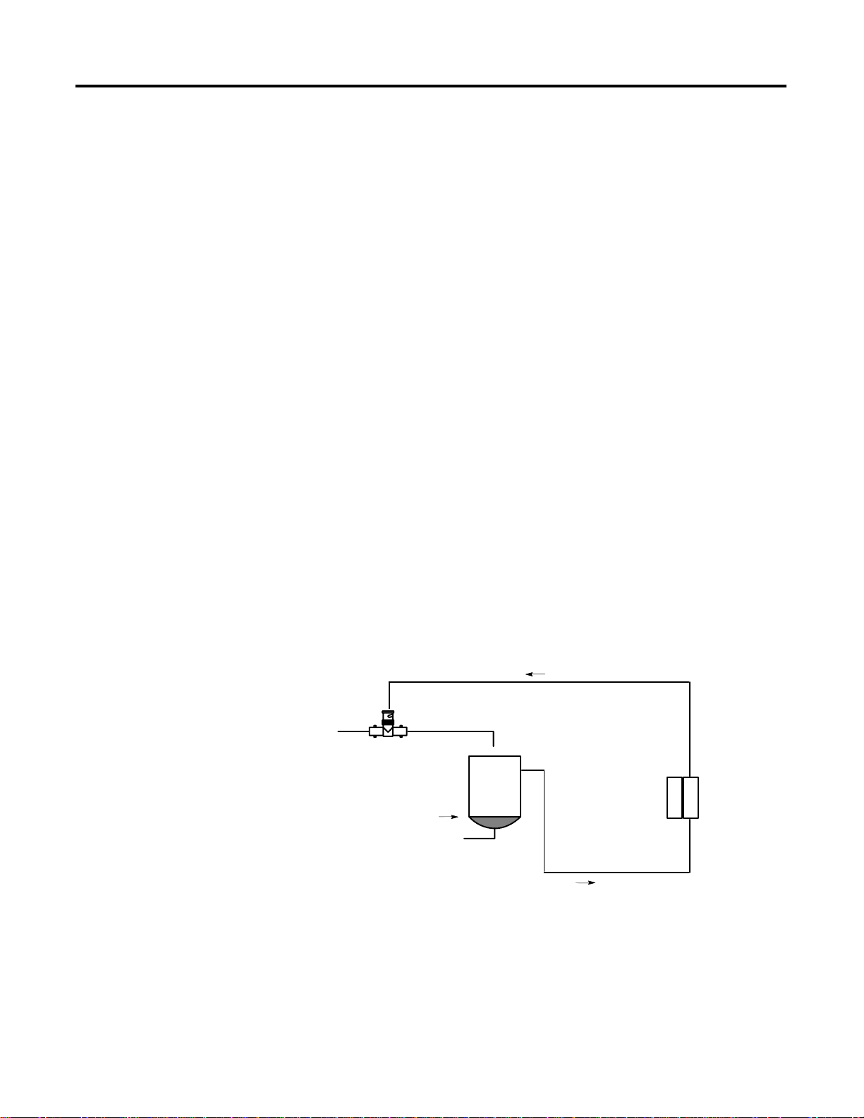
In this application, the processor controls the amount of fluid in a
holding tank by adjusting the valve opening. The valve is initially
open 100%. As the fluid level in the tank approaches the preset point,
the processor modifies the output to close the valve 90%, 80%, and so
on, continuously adjusting the valve to maintain the fluid level.
Analog output
wired to valve
Valve
Controller
Level Sensor
Analog input wired
to tank
Analog I/O
Module
1 Publication 1769-UM008A-EN-P - November 2001
Page 12

1-2 Overview
General Description of the Module’s Hardware and Diagnostic Features
The analog input channels convert and digitally store analog data for
retrieval by controllers, such as the MicroLogix™ 1500 and
CompactLogix, and from network adapters like the 1769-ADN (Series
B) DeviceNet Adapter. The module supports connections from any
combination of up to four voltage or current analog sensors. The four
high-impedance input channels can be wired as either single-ended or
differential inputs.
The output channels provide two single-ended analog outputs, each
individually configurable for voltage or current.
The module provides the following input/output types/ranges:
Table 1.1 Normal and Full Input and Output Ranges
Normal Operating Range
0 to +10V dc 0.0 to +10.5V dc
0 to 20 mA 0 to 21 mA
(1) The module provides an overrange band of 0.5V for the 0 to 10V range and 1 mA for the 0 to 20 mA
range.
Full Module Range
(1)
The modules provide the data as raw/proportional data. If scaling to
engineering units is required, it must be done in your control
program.
Hardware Features
The module has a removable terminal block. The module’s four input
channels can be wired as either single-ended or differential inputs.
The module’s two output channels are single-ended only. Module
configuration is done via proper wiring of the I/O and the controller’s
programming software. In addition, some controllers support
configuration via the user program. In either case, the module
configuration is stored in the memory of the controller. Refer to your
controller’s user manual for more information.
Publication 1769-UM008A-EN-P - November 2001
Page 13
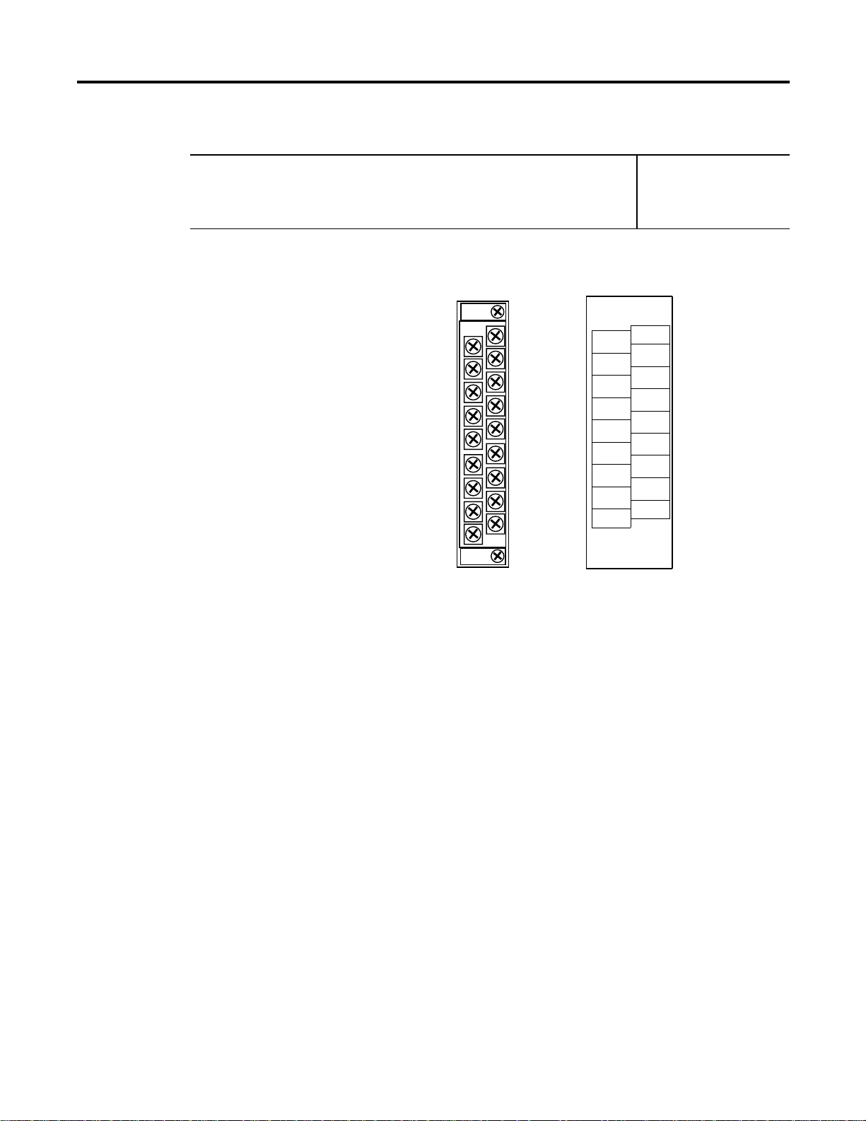
Overview 1-3
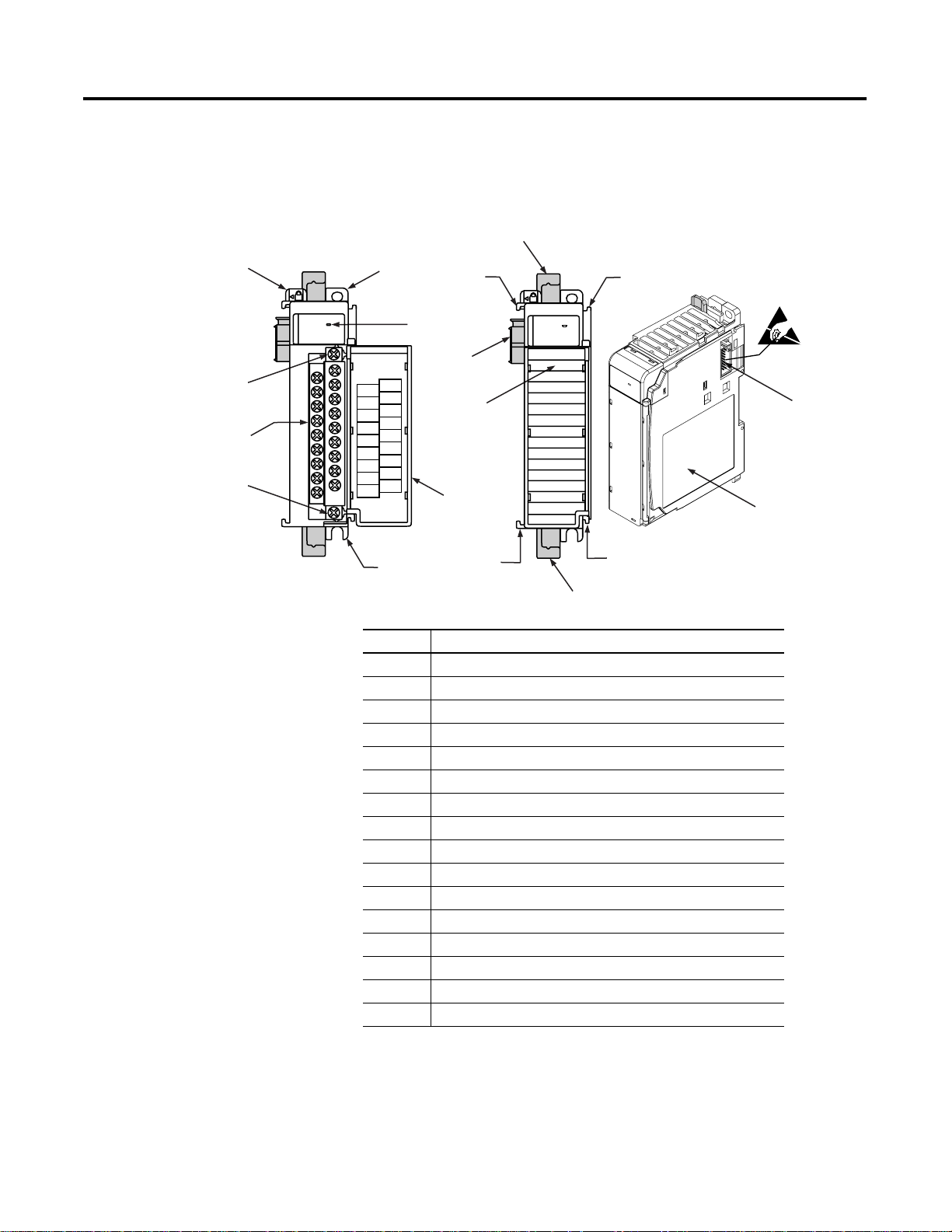
The following illustration shows the hardware features of the Compact
combination analog I/O module.
8a
10a
10
10b
1
OK
Analog
2a
DANGER
Do Not Remove RTB Under Power
Unless Area is Non-Hazardous
0
in
V
+
1
in
V
/I in
V
-
1
/I in
V
1
I in
+
1
I in
2
in
V
+
3
in
V
/I in
V
-
3
/I in
V
2
I in
+
3
I in
G
N
A
m
o
C
L
G
N
A
m
o
C
t 0
u
o
V
+
t 1
u
o
V
t 0
u
I o
+
t 1
u
I o
Ensure Adjacent
Bus Lever is Unlatched/Latched
Before/After
Removing/Inserting Module
O
X
4
-IF
9
6
7
1
2b
7a
3
OK
Analog
7a
5a
+
-
0
+
+
-
2
+
L
+
+
9
4
2
F
7b
7b
5b
6
8b
Item Description
1 bus lever (with locking function)
2a upper panel mounting tab
2b lower panel mounting tab
3 green module status OK LED
4 module door with terminal identification label
5a movable bus connector (bus interface) with female pins
5b stationary bus connector (bus interface) with male pins
6 nameplate label
7a upper tongue-and-groove slots
7b lower tongue-and-groove slots
8a upper DIN rail latch
8b lower DIN rail latch
9 write-on label for user identification tags
10 removable terminal block (RTB) with finger-safe cover
10a RTB upper retaining screw
10b RTB lower retaining screw
Publication 1769-UM008A-EN-P - November 2001
Page 14

1-4 Overview
General Diagnostic Features
The module contains diagnostic features that can help you identify the
source of problems that may occur during power-up or during normal
channel operation. These power-up and channel diagnostics are
explained in Chapter 5, Module Diagnostics and Troubleshooting.
Overview of the Analog System
The module communicates to the controller through the bus interface.
The module also receives 5 and 24V dc power through the bus
interface.
You can install as many analog modules as your power supply can
support. However, the 1769-IF4XOF2 module has a power supply
distance rating of 8, which means that it may not be located more than
8 modules away from the system power supply. The illustration below
shows how power supply distance is determined.
MicroLogix 1500 Controller
with Integrated System
Power Supply
OR
Compact I/O
Compact I/O
1
234
Compact I/O
Compact I/O
End Cap or Cable
Power Supply Distance
Publication 1769-UM008A-EN-P - November 2001
Adapter
Compact I/O
or I/O Communication
CompactLogix Controller
Compact I/O
Compact I/O
System Power Supply
Compact I/O
(e.g. 1769-PA2)
1123432
Compact I/O
Compact I/O
Power Supply Distance
End Cap or Cable
Page 15

Overview 1-5
System Operation
At power-up, the module performs a check of its internal circuits,
memory, and basic functions. During this time, the module status LED
remains off. If no faults are found during power-up diagnostics, the
module status LED is turned on.
After power-up checks are complete, the module waits for valid
channel configuration data. If an invalid configuration is detected, the
module generates a configuration error. Once a channel is properly
configured and enabled, it begins the analog-to-digital or
digital-to-analog conversion process.
Input Channels
Each time an input channel is read by the module, that analog data
value is tested by the module for an over-range condition (e.g. input
voltage greater than 10V dc). If such a condition is detected, a unique
bit is set in the channel status word. The channel status word is
described in Input Data File on page 4-3.
The controller reads the analog data from the module. This typically
occurs at the end of the program scan or when commanded by the
control program. If the controller and the module determine that the
bus data transfer was made without error, the data is used in your
control program.
Output Channels
The module monitors output channels for over-range conditions. If
such a condition is detected, a unique bit is set in the channel status
word. The channel status word is described in Output Data File on
page 4-7.
The module receives proportional binary values from the bus master
(e.g. controller). This typically occurs at the end of the program scan
or when commanded by the control program. If the controller and the
module determine that the bus transfer was completed without error,
the module converts the data to an analog output signal.
Publication 1769-UM008A-EN-P - November 2001
Page 16
1-6 Overview
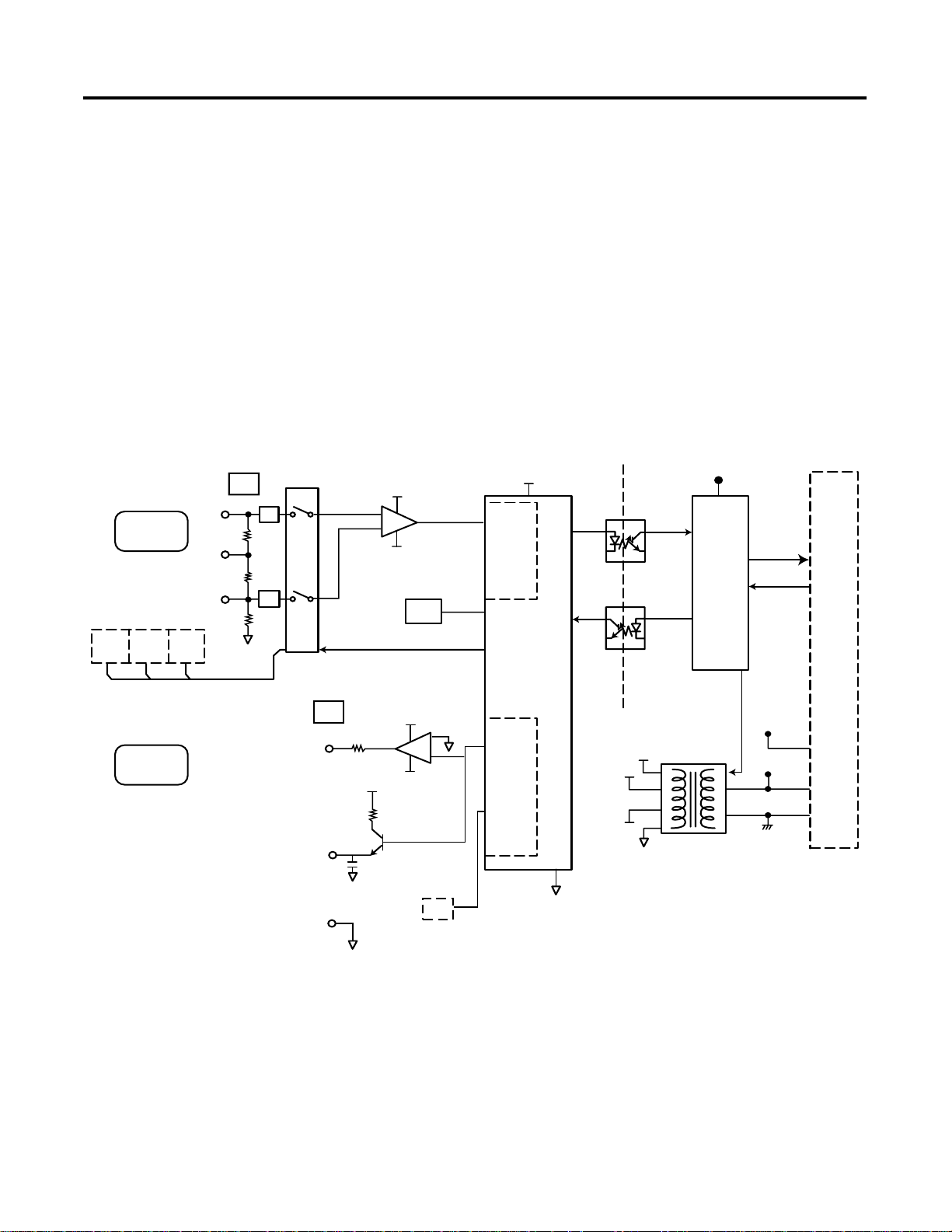
Input
Vin+
Iin+
CH0
Module Operation
Module Block Diagram
The module’s input channel circuitry consists of four differential
analog inputs multiplexed into a single analog-to-digital (A/D)
converter. The A/D converter reads the selected input signal and
converts it to a digital value which is presented to the controller. The
multiplexer sequentially switches each input channel to the module’s
A/D converter. The module’s output channel uses a digital-to-analog
(D/A) converter to read the digital output data from the controller and
convert it to an analog output signal. See the block diagram below.
Galvanic
Isolation
TXD
VA2
VA3
VA1 VS1
AIN+
A/D
(same as CH0)
CH1 CH2 CH3
Output
V/Iin-
A-GND
Multiplexer
CH0
Vout+
Iout+
A-GND
ANLG COM
A-GND
Vref
Channel Select
VA2
VA3
VA2
CH1
(same as CH0)
VREF
D/A
MCU
A-GND
RXD
VA2
VA3
VA1
A-GND
ASIC
DC/DC
Power
Supply
Bus
VS1
VS2
S-GND
Publication 1769-UM008A-EN-P - November 2001
Module Calibration
The module’s input/output channel calibration is guaranteed by its
design. No field calibration is required.
Page 17

Quick Start for Experienced Users
Chapter
2
Before You Begin
Required Tools and Equipment
This chapter can help you to get started using the analog module. We
base the procedures here on the assumption that you have an
understanding of Allen-Bradley controllers. You should understand
electronic process control and be able to interpret the ladder logic
instructions required to generate the electronic signals that control your
application.
Because it is a start-up guide for experienced users, this chapter does not
contain detailed explanations about the procedures listed. It does,
however, reference other chapters in this book where you can get more
information about applying the procedures described in each step.
If you have any questions or are unfamiliar with the terms used or
concepts presented in the procedural steps, always read the referenced
chapters and other recommended documentation before trying to apply
the information.
Have the following tools and equipment ready:
• medium blade or cross-head screwdriver
• analog input or output device
• shielded, twisted-pair cable for wiring (Belden™ 8761 or equivalent)
• controller (for example, a MicroLogix™ 1500 controller)
• analog combination (1769-IF4XOF2) module
• programming device and software (for example, RSLogix 500™)
1 Publication 1769-UM008A-EN-P - November 2001
Page 18
2-2 Quick Start for Experienced Users
What You Need To Do
Step 1:
This chapter covers:
• Verify power supply is adequate on page 2-2
• Attach and lock the module. on page 2-2
• Mount the I/O bank. on page 2-3
• Wire the module. on page 2-4
• Configure the module on page 2-5
• Start the system. on page 2-6
• Monitor the module status. on page 2-6
Verify power supply is adequate
Ensure that your power supply has sufficient current output to
support your system configuration. The modules maximum current
draw is shown below.
Module 5V dc 24V dc
1769-IF4XOF2 120 mA 160 mA
Reference
Chapter 3
(Installation and Wiring)
Step 2:
TIP
Attach and lock the module.
a. Check that the bus lever of the module to be installed is in the
unlocked (fully right) position.
b. Use the upper and lower tongue-and-groove slots to secure the
modules together (or to a controller).
c. Move the module back along the tongue-and-groove slots until
the bus connectors line up with each other.
d. Push the bus lever back slightly to clear the positioning tab. Use
your fingers or a small screwdriver.
The module cannot be located more than 8 modules
away from the system power supply.
Reference
Chapter 3
(Installation and Wiring)
Publication 1769-UM008A-EN-P - November 2001
Page 19
Quick Start for Experienced Users 2-3
e. To allow communication between the controller and module,
move the bus lever fully to the left until it clicks. Ensure it is
locked firmly in place.
ATTENTION
When attaching I/O modules, it is very important
that the bus connectors are securely locked
together to ensure proper electrical connection.
!
f. Attach an end cap terminator to the last module in the system by
using the tongue-and-groove slots as before.
g. Lock the end cap bus terminator.
ATTENTION
Remove power before removing or inserting this
module. When you remove or insert a module
with power applied, an electrical arc may occur.
!
Step 3:
Mount the I/O bank.
Be sure to observe minimum spacing guidelines on page 3-7 for
adequate ventilation.
Reference
Chapter 3
(Installation and Wiring)
Publication 1769-UM008A-EN-P - November 2001
Page 20
2-4 Quick Start for Experienced Users
Step 4:
Wire the module.
The terminal connections are shown below:
V in 1 +
V/I in 1 -
I in 1 +
V in 3 +
V/I in 3 -
I in 3 +
ANLG Com
V out 1 +
I out 1 +
V in 0 +
V/I in 0 -
I in 0 +
V in 2 +
V/I in 2 -
I in 2 +
ANLG Com
V out 0 +
I out 0 +
Reference
Chapter 3
(Installation and Wiring)
DANGER
Do Not Remove RTB Under Power
Unless Area is Non-Hazardous.
V/I in 1 I in 1 +
I in 3 +
ANLG
Com
1769-IF4XOF2
V in 0 +
V/I in 0 -
I in 0 +
V in 2 +
V/I in 2 -
I in 2+
ANLG
Com
V out 0 +
I out 0 +
V in 1 +
V in 3 +
V/I in 3 -
V out 1 +
I out 1 +
Ensure Adjacent Bus Lever is
Unlatched/Latched Before/After
Removing/Inserting Module
Be sure to follow the system wiring guidelines on page 3-10. See
the 1769-IF4XOF2 Wiring Diagram Showing Differential Inputs on
page 3-18 and the Wiring Single-ended Sensor/Transmitter Input
Types on page 3-19 for examples of wiring using differential and
single-ended inputs.
Publication 1769-UM008A-EN-P - November 2001
Page 21
Quick Start for Experienced Users 2-5
Step 5:
Table 2.1 Configuration Data File
Word
15 14 13 12 11 10 9 8 7 6 5 4 3 2 1 0
0
1
2SGN
3SGN
4SGN
5SGN
Not Used
Channel 0 Fault Value
Channel 0 Program (Idle) Value
Channel 1 Fault Value
Channel 1 Program (Idle) Value
Configure the module
The 1769-IF4XOF2 module is configured for current or voltage
operation by proper wiring of the analog I/O device to the module.
However, a channel is enabled using its configuration file.
Bit Position
(1)
Not Used
(1)
(2)
(2)
EI3 EI2 EI1 EI0
(2)
(2)
Reference
Chapter 4
(Module Data, Status, and
Configuration Channel for
1769-IF4XOF2)
(2)
FM0
EO1 EO0
FM1
(2)
0000000
0000000
0000000
0000000
PM0
PM1
(2)
Not
(1)
Used
(2)
Not
(1)
Used
PFE0
PFE1
(2)
(2)
(1) Any attempt to write a non-valid (1’s) bit configurations into any not used selection field results in a module configuration er ror.
(2) Not all controllers support these functions. Refer to your controller’s user manual for details.
The configuration file is typically modified using the programming
software configuration screen. It can also be modified through the
control program, if supported by the controller. See the configuration
file chart on page 4-8.
For an example of module configuration using MicroLogix 1500 and
RSLogix 500, see Appendix B. For an example of module
configuration using CompactLogix and RSLogix 5000, see Appendix C.
Publication 1769-UM008A-EN-P - November 2001
Page 22

2-6 Quick Start for Experienced Users
Step 6:
Step 7:
Start the system.
a. Apply power.
b. Download your program, which contains the analog module
configuration settings, to the controller and put the controller into
Run mode.
c. During a normal start-up, the module status LED turns on.
d. If the module status LED does not turn on, cycle power. If the
condition persists, replace the module.
Monitor the module status.
Module and channel configuration errors are reported to the
controller. These errors are typically reported in the controller’s I/O
status file. Check the controller’s I/O file.
Reference
Chapter 5
(Module Diagnostics and
Troubleshooting)
Reference
Chapter 6
(Module Diagnostics and
Troubleshooting)
Channel status data is also reported in the module’s input data table,
so these bits can be used in your control program to flag a channel
error. See Input Data File on page 4-3.
Publication 1769-UM008A-EN-P - November 2001
Page 23

Chapter
Installation and Wiring
This chapter tells you about:
• Compliance to European Union Directives on page 3-1
• Power Requirements on page 3-2
• General Considerations to Avoid Electrostatic Damage on page
3-2
• System Assembly on page 3-5
• Mounting the Module on page 3-6
• Field Wiring Connections on page 3-10
• Analog Input Wiring on page 3-16
• Analog Output Wiring on page 3-21
3
Compliance to European Union Directives
This product is approved for installation within the European Union
and EEA regions. It has been designed and tested to meet the
following directives.
EMC Directive
The analog modules are tested to meet Council Directive 89/336/EEC
Electromagnetic Compatibility (EMC) and the following standards, in
whole or in part, documented in a technical construction file:
• EN 50081-2
EMC – Generic Emission Standard, Part 2 - Industrial
Environment
• EN 50082-2
EMC – Generic Immunity Standard, Part 2 - Industrial
Environment
This product is intended for use in an industrial environment.
1 Publication 1769-UM008A-EN-P - November 2001
Page 24

3-2 Installation and Wiring
Low Voltage Directive
This product is tested to meet Council Directive 73/23/EEC Low
Voltage, by applying the safety requirements of EN 61131-2
Programmable Controllers, Part 2 – Equipment Requirements and
Tests.
For specific information required by EN61131-2, see the appropriate
sections in this publication, as well as the following Allen-Bradley
publications:
• Industrial Automation, Wiring and Grounding Guidelines for
Noise Immunity, publication 1770-4.1
• Automation Systems Catalog, publication B113
Power Requirements
General Considerations to Avoid Electrostatic Damage
The module receives its power through the bus interface from the +5V
dc/+24V dc system power supply.
The maximum current drawn by the module is shown in the table
below.
Module 5V dc 24V dc
1769-IF4XOF2 120 mA 160 mA
Compact I/O is suitable for use in an industrial environment when
installed in accordance with these instructions. Specifically, this
equipment is intended for use in clean, dry environments (Pollution
(1)
degree 2
) and to circuits not exceeding Over Voltage Category II
(IEC 60664-1).
(3)
(2)
Publication 1769-UM008A-EN-P - November 2001
(1) Pollution Degree 2 is an environment where, normally, only non-conductive pollution occurs except that
occasionally a temporary conductivity caused by condensation shall be expected.
(2) Over Voltage Category II is the load level section of the electrical distribution system. At this level transient
voltages are controlled and do not exceed the impulse voltage capability of the product’s insulation.
(3) Pollution Degree 2 and Over Voltage Category II are International Electrotechnical Commission (IEC)
designations.
Page 25
Installation and Wiring 3-3
Hazardous Location Considerations
This equipment is suitable for use in Class I, Division 2, Groups A, B,
C, D or non-hazardous locations only. The following WARNING
statement applies to use in hazardous locations.
WARNING
!
EXPLOSION HAZARD
• Substitution of components may impair suitability
for Class I, Division 2.
• Do not replace components or disconnect
equipment unless power has been switched off
or the area is known to be non-hazardous.
• Do not connect or disconnect components unless
power has been switched off or the area is
known to be non-hazardous.
• This product must be installed in an enclosure.
• All wiring must comply with N.E.C. article
501-4(b)
Prevent Electrostatic Discharge
ATTENTION
Electrostatic discharge can damage integrated circuits
or semiconductors if you touch bus connector pins
or the terminal block. Follow these guidelines when
you handle the module:
!
• Touch a grounded object to discharge static
potential.
• Wear an approved wrist-strap grounding device.
• Do not touch the bus connector or connector
pins.
• Do not touch circuit components inside the
module.
• If available, use a static-safe work station.
• When not in use, keep the module in its
static-shield box.
Publication 1769-UM008A-EN-P - November 2001
Page 26
3-4 Installation and Wiring
Remove Power
ATTENTION
Remove power before removing or inserting this
module. When you remove or insert a module with
power applied, an electrical arc may occur. An
electrical arc can cause personal injury or property
damage by:
!
• sending an erroneous signal to your system’s field
devices, causing unintended machine motion
• causing an explosion in a hazardous environment
Electrical arcing causes excessive wear to contacts on
both the module and its mating connector. Worn
contacts may create electrical resistance.
Reducing Electrical Noise Interference
Most applications require installation in an industrial enclosure to
reduce the effects of electrical interference. Analog inputs and outputs
are highly susceptible to electrical noise. Electrical noise coupled to
the analog inputs will reduce the performance (accuracy) of the
module.
Group your modules to minimize adverse effects from radiated
electrical noise and heat. Consider the following conditions when
selecting a location for the analog module. Position the module:
• away from sources of electrical noise such as hard-contact
switches, relays, and AC motor drives
• away from modules which generate significant radiated heat,
such as the 1769-IA16. Refer to the module’s heat dissipation
specification.
In addition, route shielded, twisted-pair analog input and output
wiring away from any high voltage I/O wiring.
Publication 1769-UM008A-EN-P - November 2001
Page 27
Installation and Wiring 3-5
Protecting the Circuit Board from Contamination
The printed circuit boards of the analog modules must be protected
from dirt, oil, moisture, and other airborne contaminants. To protect
these boards, the system must be installed in an enclosure suitable for
the environment. The interior of the enclosure should be kept clean
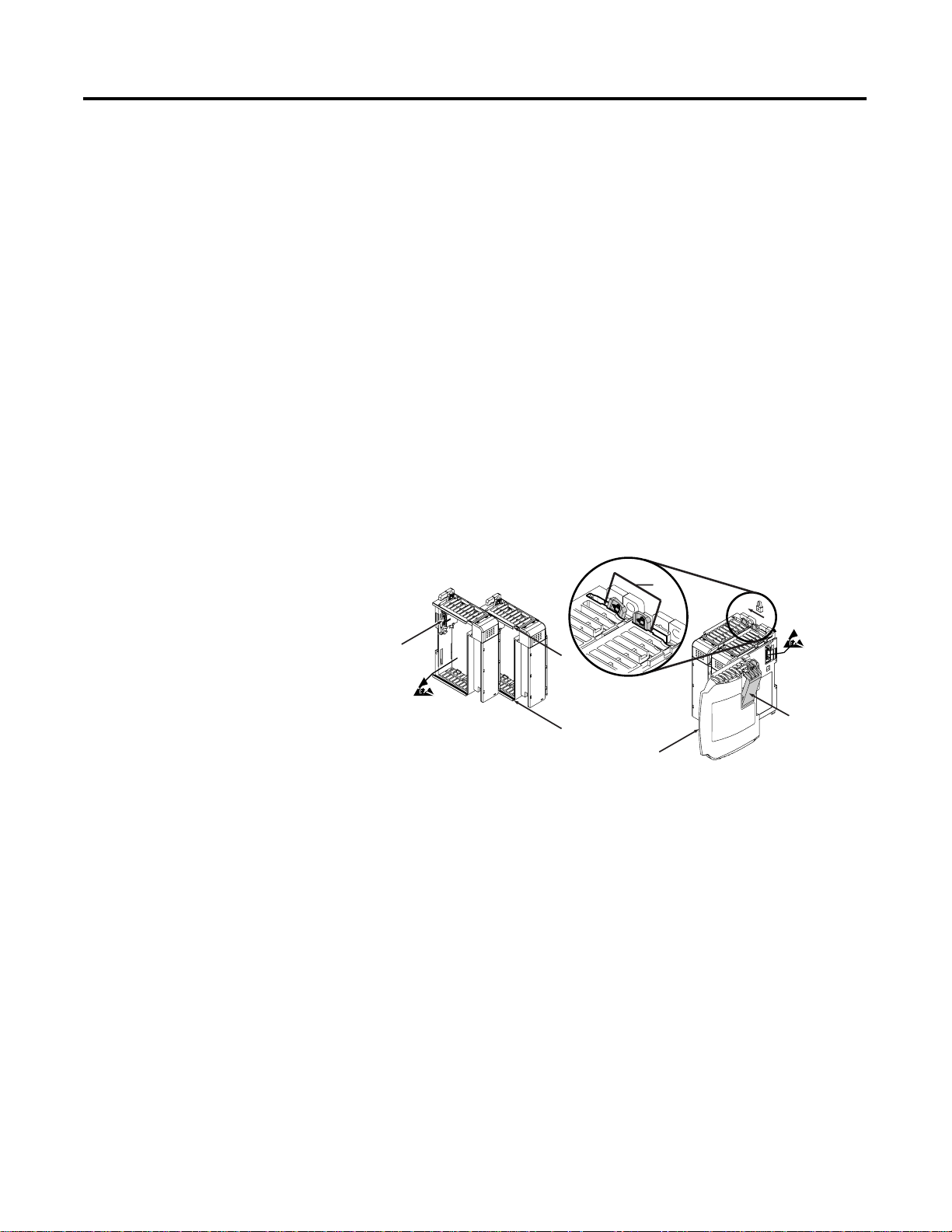
and the enclosure door should be kept closed whenever possible.
System Assembly
The module can be attached to the controller or an adjacent I/O
module or power supply before or after mounting. For mounting
instructions, see Panel Mounting Using the Dimensional Template on
page 3-7, or DIN Rail Mounting on page 3-8. To work with a system
that is already mounted, see Replacing a Single Module within a
System on page 3-9.
The following procedure shows you how to assemble the Compact
I/O system.
C
D
B
A
A
E
F
1. Disconnect power.
2. Check that the bus lever of the module to be installed is in the
unlocked (fully right) position.
3. Use the upper and lower tongue-and-groove slots (A) to secure
the modules together (or to a controller or power supply).
4. Move the module back along the tongue-and-groove slots until
the bus connectors (B) line up with each other.
5. Push the bus lever back slightly to clear the positioning tab (C).
Use your fingers or a small screwdriver.
Publication 1769-UM008A-EN-P - November 2001
Page 28
3-6 Installation and Wiring
6. To allow communication between the controller and module,
move the bus lever fully to the left (D) until it clicks. Ensure it is
locked firmly in place.
Mounting the Module
ATTENTION
When attaching I/O modules, it is very
important that the bus connectors are securely
locked together to ensure proper electrical
connection.
!
7. Attach an end cap terminator (E) to the last module in the
system by using the tongue-and-groove slots as before.
8. Lock the end cap bus terminator (F).
IMPORTANT
ATTENTION
A 1769-ECR or 1769-ECL right or left end cap
must be used to terminate the end of the
communication bus.
During panel or DIN rail mounting of all devices, be
sure that all debris (metal chips, wire strands, etc.) is
kept from falling into the module. Debris that falls
into the module could cause damage on power up.
Publication 1769-UM008A-EN-P - November 2001
!
Page 29
Installation and Wiring 3-7
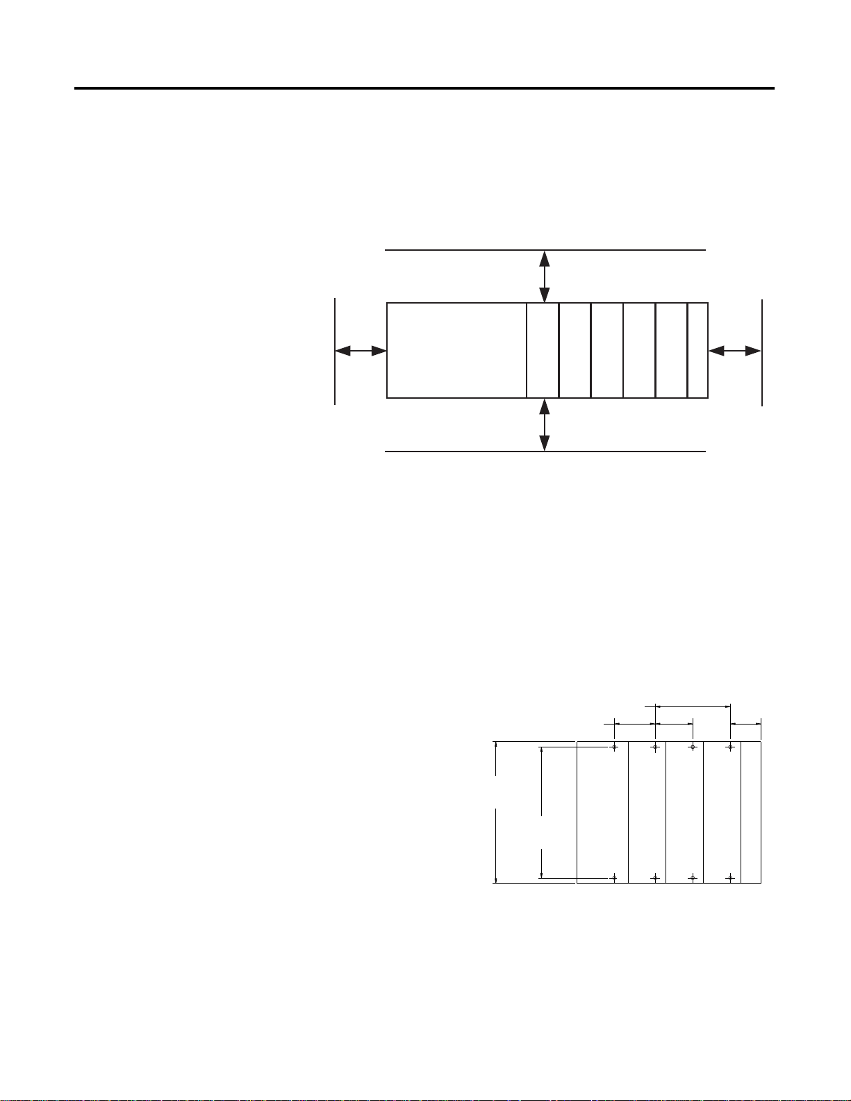
Minimum Spacing
Maintain spacing from enclosure walls, wireways, adjacent equipment,
etc. Allow 50 mm (2 in.) of space on all sides for adequate ventilation,
as shown below:
Top
Side Side
Host Controller
Compact I/O
Bottom
Compact I/O
Compact I/O
Compact I/O
End Cap
Compact I/O
Panel Mounting
Mount the module to a panel using two screws per module. Use M4
or #8 panhead screws. Mounting screws are required on every
module.
Panel Mounting Using the Dimensional Template
For more than 2 modules: (number of modules-1) X 35 mm (1.38 in.).
Refer to host controller documentation for this dimension.
35
(1.38)
28.5
(1.12)
NOTE: All dimensions are in mm (inches).
Hole spacing tolerance: ±0.04 mm (0.016 in.).
132
(5.197)
122.6±0.2
(4.826±0.008)
Compact I/O
Compact I/O
Compact I/O
Host Controller
Publication 1769-UM008A-EN-P - November 2001
Right End Cap
Page 30

3-8 Installation and Wiring
Panel Mounting Procedure Using Modules as a Template
The following procedure allows you to use the assembled modules as
a template for drilling holes in the panel. Due to module mounting
hole tolerance, it is important to follow these procedures:
1. On a clean work surface, assemble no more than three modules.
2. Using the assembled modules as a template, carefully mark the
center of all module-mounting holes on the panel.
3. Return the assembled modules to the clean work surface,
including any previously mounted modules.
4. Drill and tap the mounting holes for the recommended M4 or #8
screw.
5. Place the modules back on the panel, and check for proper hole
alignment.
6. Attach the modules to the panel using the mounting screws.
TIP
7. Repeat steps 1 to 6 for any remaining modules.
If mounting more modules, mount only the
last one of this group and put the others aside.
This reduces remounting time during drilling
and tapping of the next group.
DIN Rail Mounting
The module can be mounted using the following DIN rails:
35 x 7.5 mm (EN 50 022 - 35 x 7.5) or 35 x 15 mm (EN 50 022 - 35 x
15).
Before mounting the module on a DIN rail, close the DIN rail latches.
Press the DIN rail mounting area of the module against the DIN rail.
The latches will momentarily open and lock into place.
Publication 1769-UM008A-EN-P - November 2001
Page 31

Installation and Wiring 3-9
Replacing a Single Module within a System
The module can be replaced while the system is mounted to a panel
(or DIN rail). Follow these steps in order:
1. Remove power. See attention note on 3-4.
2. On the module to be removed, remove the upper and lower
mounting screws from the module (or open the DIN latches
using a flat-blade or phillips-style screwdriver).
3. Move the bus lever to the right to disconnect (unlock) the bus.
4. On the right-side adjacent module, move its bus lever to the
right (unlock) to disconnect it from the module to be removed.
5. Gently slide the disconnected module forward. If you feel
excessive resistance, check that the module has been
disconnected from the bus, and that both mounting screws have
been removed (or DIN latches opened).
TIP
It may be necessary to rock the module slightly
from front to back to remove it, or, in a
panel-mounted system, to loosen the screws of
adjacent modules.
6. Before installing the replacement module, be sure that the bus
lever on the module to be installed and on the right-side
adjacent module are in the unlocked (fully right) position.
7. Slide the replacement module into the open slot.
8. Connect the modules together by locking (fully left) the bus
levers on the replacement module and the right-side adjacent
module.
9. Replace the mounting screws (or snap the module onto the DIN
rail).
Publication 1769-UM008A-EN-P - November 2001
Page 32

3-10 Installation and Wiring
Field Wiring Connections
Grounding
This product is intended to be mounted to a well-grounded mounting
surface such as a metal panel. Additional grounding connections from
the module’s mounting tabs or DIN rail (if used) are not required
unless the mounting surface cannot be grounded. Refer to Industrial
Automation Wiring and Grounding Guidelines, Allen-Bradley
publication 1770-4.1, for additional information.
System Wiring Guidelines
Consider the following when wiring your system:
General
• All module commons (ANLG COM) are connected in the analog
module. The analog common (ANLG COM) is not connected to
earth ground inside the module.
• Channels are not isolated from each other.
• Use Belden™ 8761, or equivalent, shielded wire.
• Under normal conditions, the drain wire and shield junction
must be connected to earth ground via a panel or DIN rail
mounting screw at the analog I/O module end. Keep the shield
connection to ground as short as possible.
• To ensure optimum accuracy, limit overall cable impedance by
keeping your cable as short as possible. Locate the I/O system
as close to your sensors or actuators as your application will
permit.
(2)
(1)
Publication 1769-UM008A-EN-P - November 2001
Inputs
• If multiple power supplies are used with analog inputs, the
power supply commons must be connected.
• The module does not provide loop power for analog inputs. Use
a power supply that matches the input transmitter specifications.
• Differential analog inputs are more immune to noise than
single-ended analog inputs.
• Voltages on Vin+, V/Iin-, and Iin+ of the module must be within
0 to +10V dc of analog common.
(1) In environments where high-frequency noise may be present, it may be necessary to directly ground cable shields to earth at
the module end and via a 0.1µF capacitor at the sensor end.
(2) Cable length over 50 meters may impact accuracy., For details, refer to the
publication 1769-UM008A-EN-P.
Compact Combination Analog I/O Module
,
Page 33

Installation and Wiring 3-11
Outputs
• Voltage outputs (Vout 0+ and Vout 1+) of the module are
referenced to ANLG COM. Load resistance for a voltage output
channel must be equal to or greater than 1K
• Current outputs (Iout 0+ and Iout 1+) of the module source
current that returns to ANLG COM. Load resistance for a current
output channel must remain between 0 and 300
Ω.
Ω.
ATTENTION
Be careful when stripping wires. Wire fragments
that fall into a module could cause damage at
power up. Once wiring is complete, ensure the
module is free of all metal fragments.
!
Effect of Transducer/Sensor and Cable Length Impedance on Voltage Input
Accuracy
For voltage inputs, the length of the cable used between the
transducer/sensor and the module can affect the accuracy of the data
provided by the module.
RcRs
+
Vs
V in
-
Rc
Ri
Where:
Rc = DC resistance of the cable (each conductor) depending on
cable length
Rs = Source impedance of analog transducer/sensor input
Ri = Impedance of the voltage input (150 K
Vs = Voltage source (voltage at the transducer/sensor input
device)
Vin = Measured potential at the module input
%Ai = Percent added inaccuracy in a voltage-based system due
to source and cable impedance.
Ri Vs
Vin
=
-------------------------------------------------------
Rs
×[]
2
Rc
++[]
×()
Ri
Publication 1769-UM008A-EN-P - November 2001
Ω)
Page 34

3-12 Installation and Wiring
For example, for Belden 8761 two conductor, shielded cable:
Rc = 16
Ω/1000 ft
Rs = 0 (ideal source)
Table 3.1 Effect of Cable Length on Input Accuracy
Length of Cable (m) dc resistance of the
cable, Rc (ΩΩΩΩ)
50 2.625 0.00350%
100 5.25 0.00700%
200 10.50 0.01400%
300 15.75 0.02100%
Vin
%
Ai
–
1
---------
Vs
Accuracy impact at the
input module
100×=
As input source impedance (Rs) and/or resistance (dc) of the cable
(Rc) get larger, system accuracy decreases. If you determine that the
inaccuracy error is significant, implementing the following equation in
the control program can compensate for the added inaccuracy error
due to the impedance of the source and cable.
Publication 1769-UM008A-EN-P - November 2001
TIP
2
Rc
Vs Vin
++[]
Rs
×=
-------------------------------------------------------
×()
Ri
Ri
In a current loop system, source and cable
impedance do not impact system accuracy.
Page 35

Installation and Wiring 3-13
Effect of Device and Cable Output Impedance on Output Accuracy
The maximum value of the output impedance is shown in the
example below, because it creates the largest deviation from an ideal
voltage source.
RcRs
+
Vs
-
Where:
Rc = DC resistance of the cable (each conductor)
depending on cable length
V in
Rc
Ri
Rs = Source impedance of the 1769-IF4XOF2 output (10
Ri = Impedance of the voltage input (150 K
Ω for the voltage input
Ω)
channel of the 1769-IF4XOF2)
Vs = Voltage at the output
Vin = Measured potential at the module input
%Ai = Percent added inaccuracy in a voltage-based
system due to source and cable impedance.
Ri Vs
Vin
-------------------------------------------------------=
Rs
×[]
2
Rc
++[]
×()
Ri
For example, for Belden 8761 two conductor, shielded cable and an
input channel:
Rc = 16
Rs = 10
Ω/1000 ft
Ω
Vin
%
Ai
–
1
---------
Vs
100×=
Ri = 150 KΩ
Table 3.2 Effect of Output Impedance and Cable Length on Accuracy
Length of Cable (m) dc resistance of the cable
Rc (ΩΩΩΩ)
50 2.625 0.01017%
100 5.25 0.01366%
200 10.50 0.02066%
300 15.75 0.02766%
Accuracy impact at the
input module
Publication 1769-UM008A-EN-P - November 2001
Page 36

3-14 Installation and Wiring
As output impedance (Rs) and/or resistance (dc) of the cable (Rc) get
larger, system accuracy decreases. If you determine that the
inaccuracy error is significant, implementing the following equation in
the control program can compensate for the added inaccuracy error
due to the impedance of the output module and cable.
Rs
2
Rc
Vs Vin
-------------------------------------------------------×=
Ri
×()
++[]
Ri
TIP
In a current loop system, source and cable
impedance do not impact system accuracy.
Removing the Finger-Safe Terminal Block
When wiring field devices to the module, it is not necessary to remove
the terminal block. If you remove the terminal block, use the write-on
label on the side of the terminal block to identify the module slot
location and type.
SLOT # _____
MODULE TYPE ______
Publication 1769-UM008A-EN-P - November 2001
Page 37

Installation and Wiring 3-15
To remove the terminal block, loosen the upper and lower retaining
screws. The terminal block will back away from the module as you
remove the screws. When replacing the terminal block, torque the
retaining screws to 0.46 Nm (4.1 in-lbs).
upper retaining screw
lower retaining screw
wiring the finger-safe
terminal block
Wiring the Finger-Safe Terminal Block
When wiring the terminal block, keep the finger-safe cover in place.
1. Loosen the terminal screws to be wired.
2. Route the wire under the terminal pressure plate. You can use
the bare wire or a spade lug. The terminals will accept a 6.35
mm (0.25 in.) spade lug.
TIP
The terminal screws are non-captive.
Therefore, it is possible to use a ring lug
[maximum 1/4 inch o.d. with a 0.139 inch
minimum i.d. (M3.5)] with the module.
3. Tighten the terminal screw making sure the pressure plate
secures the wire. Recommended torque when tightening
terminal screws is 0.68 Nm (6 in-lbs).
TIP
If you need to remove the finger-safe cover,
insert a screw driver into one of the square
wiring holes and gently pry the cover off. If you
wire the terminal block with the finger-safe cover
removed, you will not be able to put it back on
the terminal block because the wires will be in
the way.
Publication 1769-UM008A-EN-P - November 2001
Page 38

3-16 Installation and Wiring
Wire Size and Terminal Screw Torque
Each terminal accepts up to two wires with the following restrictions:
Wire Type Wire Size Terminal Screw Torque Retaining Screw Torque
Solid Cu-90°C (194°F) #14 to #22 AWG 0.68 Nm (6 in-lbs) 0.46 Nm (4.1 in-lbs)
Stranded Cu-90°C (194°F) #16 to #22 AWG 0.68 Nm (6 in-lbs) 0.46 Nm (4.1 in-lbs)
Analog Input Wiring
ATTENTION
To prevent shock hazard, care should be taken when
wiring the module to analog signal sources. Before
wiring any analog module, disconnect power from
the system power supply and from any other source
to the analog module.
!
After the analog module is properly installed, follow the wiring
procedure below. To ensure proper operation and high immunity to
electrical noise, always use Belden™ 8761 (shielded, twisted-pair) or
equivalent wire.
ATTENTION
!
signal wire
signal wire
When wiring an analog input, take care to avoid
connecting a voltage source to a channel configured
for current input. Improper module operation or
damage to the voltage source can occur.
Never connect a voltage or current source to an
analog output channel.
Cut foil shield
and drain wire
signal wire
drain wire
cable
foil shield
signal wire
Publication 1769-UM008A-EN-P - November 2001
To wire your module follow these steps.
1. At each end of the cable, strip some casing to expose the
individual wires.
2. Trim the signal wires to 2-inch lengths. Strip about 3/16 inch (5
mm) of insulation away to expose the end of the wire.
Page 39

Installation and Wiring 3-17
ATTENTION
Be careful when stripping wires. Wire fragments
that fall into a module could cause damage at
power up.
!
3. At one end of the cable, twist the drain wire and foil shield
together.
Under normal conditions, this drain wire and shield junction
must be connected to earth ground, via a panel or DIN rail
mounting screw at the analog I/O module end. Keep the length
of the drain wire as short as possible.
In environments where high frequency noise may be present,
the cable shields should be grounded via a 0.1 µF capacitor at
the end using the data. In other words, for analog inputs, the
cable shield should be grounded via the 0.1 µF capacitor at the
analog module end. For analog outputs, the cable shield should
be grounded via a 0.1 µF capacitor at the load end.
4. At the other end of the cable, cut the drain wire and foil shield
back to the cable.
5. Connect the signal wires to the terminal block as shown in
Analog Input Wiring on page 3-16 and Analog Output Wiring on
page 3-21. Connect the other end of the cable to the analog
input or output device.
6. Repeat steps 1 through 5 for each channel on the module.
Publication 1769-UM008A-EN-P - November 2001
Page 40

3-18 Installation and Wiring
Terminal Door Label
A removable, write-on label is provided with the module. Remove the
label from the door, mark the identification of each terminal with
permanent ink, and slide the label back into the door. Your markings
(ID tag) will be visible when the module door is closed.
DANGER
Do Not Remove RTB Under Power
Unless Area is Non-Hazardous.
Com
1769-IF4XOF2
V in 0 +
V/I in 0 -
I in 0 +
V in 2 +
V/I in 2 -
I in 2+
ANLG
Com
V out 0 +
I out 0 +
V in 1 +
V/I in 1 -
I in 1 +
V in 3 +
V/I in 3 -
I in 3 +
ANLG Com
V out 1 +
I out 1 +
V in 0 +
V/I in 0 -
I in 0 +
V in 2 +
V/I in 2 I in 2 +
ANLG Com
V out 0 +
I out 0 +
V in 1 +
V/I in 1 I in 1 +
V in 3 +
V/I in 3 -
I in 3 +
ANLG
V out 1 +
I out 1 +
Ensure Adjacent Bus Lever is
Unlatched/Latched Before/After
Removing/Inserting Module
Wiring Diagram Showing Differential Inputs
1769-IF4XOF2 Terminal Block
V in 1+
V in 0+
V/I in 0-
V/I in 1 -
I in 1+
V in 3+
V/I in 3 -
I in 0+
V in 2 +
V/I in 2-
earth ground the shield
locally at
the module
I in 2+
I in 3+
ANLG Com
Belden 8761 cable (or equivalent)
ANLG Com
V out 1+
I out 1+
(1) All analog commons (ANLG Com) are internally connected.
(2) If multiple power supplies are used, the commons must have the same ground reference.
(3) User Belden 8761 cable (or equivalent) for wiring analog I/O.
V out 0+
I out 0+
+
differential voltage
–
transmitter
Publication 1769-UM008A-EN-P - November 2001
Page 41

Wiring Single-ended Sensor/Transmitter Input Types
Installation and Wiring 3-19
1769-IF4XOF2 Terminal Block
Sensor/
Tra ns mi tt er
Power
Supply
(1) The sensor power supply must be rated Class 2.
(2) All analog commons (ANLG Com) are internally connected.
(3) If multiple power supplies are used, the commons must have the same ground
reference.
(4) User Belden 8761 cable (or equivalent) for wiring analog I/O.
+
-
(1)
Current
Transmitter
Signal
+
Voltage Transmitter
Ground Signal
+
V in 0+
I in 0+
V/I in 0 -
V in 1+
I in 1+
V/I in 1-
V in 2+
I in 2+
V/I in 2V in 3+
I in 3+
V/I in 3ANLG Com
ANLG Com
V out 0+
I out 0+
V out 1+
I out 1 +
Publication 1769-UM008A-EN-P - November 2001
Page 42

3-20 Installation and Wiring
Wiring Mixed Transmitter Input Types
Single-ended
Voltage
Transmitter
–
Differential
Voltage
Transmitter
Supply
Differential
Current
Transmitter
–
Supply
2-Wire
Current
Tra ns mi tt er
Sensor/
Tra ns mi tt er
Power Supply
Signal
+
+
Signal
–
+–
+
Signal
–
+
Signal
+
1769-IF4XOF2 Terminal Block
V in 0+
I in 0+
V/I in 0 V in 1+
I in 1+
V/I in 1-
V in 2+
I in 2+
V/I in 2V in 3+
I in 3+
V/I in 3-
ANLG Com
ANLG Com
V out 0+
I out 0+
V out 1+
I out 1 +
+
(1)
–
(1) The sensor power supply must be rated Class 2.
(2) All analog commons (ANLG Com) are internally connected.
(3) If multiple power supplies are used, the commons must have the same ground reference.
(4) User Belden 8761 cable (or equivalent) for wiring analog I/O.
Publication 1769-UM008A-EN-P - November 2001
Page 43

Analog Output Wiring
ATTENTION
!
Voltage Load
Current Load
Installation and Wiring 3-21
To prevent shock hazard, care should be taken when
wiring the module to analog signal sources. Before
wiring any analog module, disconnect power from
the system power supply and from any other source
to the analog module.
V in 0+
I in 0+
V/I in 0 V in 1+
I in 1+
V/I in 1-
V in 2+
I in 2+
V/I in 2V in 3+
I in 3+
V/I in 3-
(1)
ANLG Com
(1)
Earth Ground
ANLG Com
V out 0+
I out 0+
V out 1+
I out 1 +
Earth Ground
(1) All analog common terminals (ANLG Com) are internally connected in the module.
Publication 1769-UM008A-EN-P - November 2001
Page 44

3-22 Installation and Wiring
Publication 1769-UM008A-EN-P - November 2001
Page 45

Chapter
4
1769-IF4XOF2 Module Data, Status, and
Configuration Channels
This chapter examines the 1769-IF4XOF2 module’s data table, channel
status, and channel configuration word:
• Module Addressing on page 4-1
• Input Data File on page 4-3
• Output Data File on page 4-7
• Configuration Data File on page 4-8
Module Addressing
slot e
Input Image File
slot e
Configuration
File
The following memory map shows the input, output, and
configuration image tables. Detailed information on the input image
table can be found in Input Image on page 4-3.
Memory Map
Word 0
Word 1
Word 2
Word 3
Word 4
Word 5
Word 6, bits 7 to 14
Word 7, bits 7 to 14
Word 0
Word 1
Word 2
Word 3
Word 4
Word 5
Input Image
8 words
Configuration File
6 words
Channel 0 Input Word
Channel 1 Input Word
Channel 2 Input Word
Channel 3 Input Word
Over-range Bits - Inputs
Over-range Bits - Outputs
Channel 0 Output Loopback
Channel 1 Output Loopback
Configuration Word
Configuration Word
Output Channel 0 Fault Value
Output Channel 0 Program (Idle) Value
Output Channel 1 Fault Value
Output Channel 1 Program (Idle) Value
slot e
Output Image
File
1 Publication 1769-UM008A-EN-P - November 2001
Output Image
2 words
Channel 0 Output Data Word
Channel 1 Output Data Word
Bit 15
Word 0
Word 1
Bit 0
Page 46

4-2 1769-IF4XOF2 Module Data, Status, and Configuration Channels
Input/Output/Configuration Data Registers
Data registers are available for input, output, and configuration. There
are eight input data registers, six configuration registers, and two
output data registers. The module and programming software applies
the following default values to the registers:
Table 4.1 Data Registers
Register Function Default at
C:0 Configuration Word 1 0000h 0000h
C:1 Configuration Word 2 0000h 0000h
Power-Up
Programming Software
Default Down Load
C:2 Configuration - Channel 0
Fault Value
C:3 Configuration - Channel 0
Program Value
C:4 Configuration - Channel 1
Fault Value
C:5 Configuration - Channel 1
Program Value
I:0 Channel 0 Input Word 0000h
I:1 Channel 1 Input Word 0000h
I:2 Channel 2 Input Word 0000h
I:3 Channel 3 Input Word 0000h
I:4 Input Channel Over-range 0000h
I:5 Output Channel Over-range 0000h
I:6 Channel 0 Output Data Echo 0000h
I:7 Channel 1 Output Data Echo 0000h
O:0 Channel 0 Output Word 0000h 0000h
O:1 Channel 1 Output Word 0000h 0000h
0000h 0000h
0000h 0000h
0000h 0000h
0000h 0000h
Publication 1769-UM008A-EN-P - November 2001
Page 47

1769-IF4XOF2 Module Data, Status, and Configuration Channels 4-3
Input Data File
The input data file provides access to analog input data for use in the
control program. Input data resolution is 8 bits with the least
significant 7 bits (0 to 6) permanently set to zero (0) by the module. In
addition, over-range indication for the input and output channels, and
output data feedback is provided as described below.
Table 4.2 Input Data File
Bit Position
Word
(1) All unused bits are set to 0 by the module.
15 14 13 12 11 10 9 8 7 6 5 4 3 2 1 0
0 SGN Analog Input Data Value Channel 0 0 0 0 0 0 0 0
1 SGN Analog Input Data Value Channel 1 0 0 0 0 0 0 0
2 SGN Analog Input Data Value Channel 2 0 0 0 0 0 0 0
3 SGN Analog Input Data Value Channel 3 0 0 0 0 0 0 0
4
5
Not
Used
6 SGN Output Data Echo/Loopback for Output Channel 0 0 0 0 0 0 0 0
7 SGN Output Data Echo/Loopback for Output Channel 1 0 0 0 0 0 0 0
(1)
H0 Not
Used
H1
(1)
Not Used
(1)
Not Used
(1)
I3 I2 I1 I0
E1 E0 O1 O0
Input Image
The input image file represents input channel data words I/O, and I/O
channel status bits. Input words 0 through 3 contain the converted
analog input data from the field device. Word 4, bit 1,2 and 3 are the
over-range flag bits for input channels 0 to 3. Word 5, bit 0 and 1 are
the over-range flag bits for output channels 0 and 1. Words 6 and 7,
bits 7 through 14 are the data echo. These words provide output
channel loopback/data echo from output channels 0 and 1 through
the input array. See Input Data File on page 4-3 for more information.
TIP
You can access information in the input image file
using the programming software configuration
screen.
Publication 1769-UM008A-EN-P - November 2001
Page 48

4-4 1769-IF4XOF2 Module Data, Status, and Configuration Channels
Input Data Words 0 through 3
All bits shown as 0 (bits 0 through 6) are always set to 0. Bits 7
through 14 contain the 8 input data bits. The table below illustrates
the format of the input data, words 0 to 3.
1514131211109876543210
SGNA7A6A5A4A3A2A1A00000000
Input Data Words 4 through 7
These words contain diagnostic and control information. For details
see Bit Definitions for Input Data below.
Bit Definitions for Input Data
Sign Bit (SGN)
The sign bit is always positive (equal to zero).
Over Input Range Flag Bits (I0 to I3)
Word 4, bits 0 to 3 (i0 to I3) contain over-range flag bits for input
channels 0 through 3 respectively. These bits can be used in the
control program for error detection. When set to 1, the bits signal that
the input signal is outside the normal operating range. However, the
module continues to convert analog data to the maximum full-range
value. When the over-range condition is cleared, the bits automatically
reset to (0).
Over Output Range Flag Bits (O0 and O1)
Word 5, bits 0 and 1 (O0 and O1) provide over-range indication for
output channels 0 and 1. These bits can be used in the control
program for error detection. When set to 1, the bits signal that the
output signal is outside the normal operating range. However, the
module continues to convert analog data to the maximum full-range
value. When the over-range condition is cleared, the bits automatically
reset to 0.
Publication 1769-UM008A-EN-P - November 2001
TIP
Under-range indication is not provided for the
1769-IF4OXF2 because zero is a valid number.
Refer to Table 4.9 Valid Input Data on page 4-14 to
view the normal operating and over-range areas.
Page 49

1769-IF4XOF2 Module Data, Status, and Configuration Channels 4-5
Invalid Data Set (Ex)
Word 5, bits 2 and 3 provide invalid output data indication for output
channels 0 and 1, respectively. When either invalid output data bit is
set to 1, it indicates that invalid output data has been sent by the
controller to that channel of the module. When this occurs, the
module sets the appropriate (Ex) flag and continues to operate with
the previously accepted data.
NOTE: Invalid data is a value outside the standard range or increment.
For example, 128, 256, etc. or by writing to bits 0 though 6 and bit 15.
Hold Last State (Hx)
Word 5, bits 12 and 14, indicates that the channel is in a hold last state
condition when set to 1.
IMPORTANT
Not all controllers support Hold Last State
functionality. Refer to your controller’s user manual.
Analog Output Loopback/Data Echo
Input words 6 and 7, bits 7-14, reflect the analog output data echo of
the analog value being converted by the digital/analog converter, not
necessarily the electrical state of the output terminals. They do not
reflect shorted or open outputs.
IMPORTANT
IMPORTANT
Input words 6 and 7 contain the Output Data
Echo/Loopback information for output channels 0
and 1 respectively. Bits 0 through 6 and Bit 15 of
words 6 and 7 should always be set to zero in your
control program, or the module will set the Invalid
Data Set (Ex) flag.
It is only important to use the loopback function of
input words 6 and 7 if the controller supports the
Program Mode or Fault Mode functions, and if it is
configured to use them.
Publication 1769-UM008A-EN-P - November 2001
Page 50

4-6 1769-IF4XOF2 Module Data, Status, and Configuration Channels
Input Data Resolution and Format
The following table identifies the current and voltage input ranges for
the 1769-IF4XOF2 module, and the number of significant bits
provided by the module with its single (non-programmable) filter. The
number of significant bits indicated in the table has little or no jitter
due to noise. The module’s RAW/Proportional data format presents
the value to the controller via a left justified 16-bit field, with the most
significant bit for the sign bit (which is always zero).
Table 4.3 Input Data Resolution and Format
Full Input Range RAW/Proportional Data
Significant Bits Resolution per LSB Decimal Representation of Input Count Value
0V to 10.5V dc Sign + 8 bits 41.18mV 0 to 32640 128 (1LSB)
0 mA to 21 mA Sign + 8 bits 82.35mA 0 to 32640 128 (1LSB)
Input Scaling
Example 1: Find voltage by converting raw/proportional data values
To convert a raw/proportional data value to find the voltage
being measured:
Voltage = (Input Data Value X volts/significant bit) /
(counts/significant bit)
If input data value is 32,640
Voltage = (32640 X 0.04118V) / 128
= 10.50 Volts
Example 2: Find current by converting raw/proportional data values
To convert a raw/proportional data value to find the current
being measured:
Current = (Input Data Value X amps/significant bit) /
(counts/significant bit)
If the input data value is 31,104
Current = (31,104 X 0.08235A) /128
= 20 mA
Publication 1769-UM008A-EN-P - November 2001
Page 51

1769-IF4XOF2 Module Data, Status, and Configuration Channels 4-7
Output Data File
The output file contains the module’s analog output data information.
Word 0 and 1, bits 7 through 14 contain the output data bits for
channels 0 and 1.
The output data file applies only to output data from the module as
shown in the table below.
Table 4.4 Output Data File
Bit Position
1514131211109876543210
Word
0 SGN Analog Output Data Channel 0 0000000
1 SGN Analog Output Data Channel 1 0000000
Output Data Words 0 and 1
The SGN bit of Words 0 and 1 is always zero (0). The following table
illustrates the format of the output data.
1514131211109876543210
SGNA7A6A5A4A3A2A1A00000000
IMPORTANT
Bits 0 through 6 and Bit 15 of output data words 0
and 1 should always be set to zero in your control
program. If they are not set to 0, the invalid data flag
(Ex) will be set for that channel. However the
channel will continue to operate with the previously
converted value. If a MVM (Move with Mask)
instruction is used with a mask of 7F80 (hexidecimal)
to move data to the output words, writing to bits 0
through 6 and bit 15 can be avoided.
Publication 1769-UM008A-EN-P - November 2001
Page 52

4-8 1769-IF4XOF2 Module Data, Status, and Configuration Channels
Output Data Resolution and Format
The resolution of an analog output channel depends on the output
type/range and data format selected. The following table provides
detailed resolution information for the module.
Table 4.5 Output Resolution
Full Output Range RAW/Proportional Data
Significant Bits Resolution per LSB Decimal
Representation of
Output
0V to 10.5 V dc Sign + 8 bits 41.18mV 0 to 32640 128 (1LSB)
0 mA to 21 mA Sign + 8 bits 82.35mA 0 to 32640 128 (1LSB)
Count Value
Configuration Data File
The configuration file allows you to enable or disable an input or
output channel. It also allows you to configure the operation of the
outputs during a mode change to Program or a Fault condition.
Word 0 bits 4, 5, 6 and 7 allow the individual input channels to be
enabled or disabled. Word 1 bits 4 and 5 allow the individual output
channels to be enabled or disabled.
TIP
Not all controllers support program access to the
configuration file. Refer to your controller’s user
manual.
Publication 1769-UM008A-EN-P - November 2001
Page 53

Table 4.6 Configuration Data File
15 14 13 12 11 10 9 8 7 6 5 4 3 2 1 0
Word
0
Not Used
1
2SGN
3SGN
4SGN
5SGN
Channel 0 Fault Value
Channel 0 Program (Idle) Value
Channel 1 Fault Value
Channel 1 Program (Idle) Value
(1)
Not Used
1769-IF4XOF2 Module Data, Status, and Configuration Channels 4-9
The manipulation of the bits from this file is normally done with
programming software (e.g. RSLogix 500, RSLogix 5000, RSNetworx
for DeviceNet, etc.) during initial configuration of the system. In that
case, graphical screens are typically provided by the programmer to
simplify configuration. However, some systems, like the 1769-ADN
DeviceNet Adapter, also allow the bits to be altered as part of the
control program, using communication rungs. In that case, it may be
beneficial to understand the bit arrangement.
Bit Position
EI3 EI2 EI1 EI0
(1)
(2)
(2)
(2)
(2)
EO1 EO0
0000000
0000000
0000000
0000000
FM0
FM1
(2)
(2)
PM0
PM1
(2)
Not
(1)
Used
(2)
Not
(1)
Used
PFE0
PFE1
(2)
(2)
(1) Any attempt to write a non-valid (1’s) bit configurations into any not used selection field results in a module configuration er ror.
(2) Not all controllers support these functions. Refer to your controller’s user manual for details.
Bit Definitions for Configuration Data
Sign Bit (SGN)
The sign bit is always positive (Bit 15 = zero).
Enable/Disable Input Channel (EIx)
Word 0 bits 4 to 7 (EI0 to EI3) are defined as the input channel
enable/disable bits. These bits allow individual input channels 0
through 3 to be enabled (on) or disabled (off). When a channel is not
enabled, the module provides no current or voltage input to the host
controller.
Publication 1769-UM008A-EN-P - November 2001
Page 54

4-10 1769-IF4XOF2 Module Data, Status, and Configuration Channels
Enable/Disable Output Channel (EOx)
Word 1 bits 4 and 5 (EO0 and EO1) are defined as the output channel
enable/disable bits. EOx bits allow individual output channels 0 and 1
to be enabled or disabled. When a channel is not enabled, the module
does not produce current or voltage.
TIP
To improve performance and speed, disable unused
channels.
Program/Idle Mode Selection Channel 0 and 1 (PM0 and PM1)
These bits provide Program (Idle) Mode selection for analog output
channels 0 (Word 0 Bit 2) and 1 (Word 1 Bit 2).
• Hold Last State (0) – When reset (to 0), this bit directs the
module to hold the analog output at the last converted value
when the module transitions from Run to Program Mode. This is
the default channel condition.
IMPORTANT
Hold last state is the default condition for the
module during a control system
run-to-program mode change.
Publication 1769-UM008A-EN-P - November 2001
TIP
MicroLogix 1500™ does not support the
analog output module’s default hold last state
function and resets analog outputs to zero
when the system enters the program mode.
• User-Defined Safe State (1) – When this bit is set (to 1) and the
module transitions to Program mode, the module converts the
user-specified integer value from the Channel x Program Value
Word (3 or 5) to the appropriate analog output.
Fault Mode Selection Channel 0 and 1 (FM0 and FM1)
FM0 and FM1 bits provide Fault Mode selection for analog output
channels 0 (Word 0 Bit 3) and 1 (Word 1 Bit 3). When this selection is
disabled [the bit is reset (0)] and the system transitions from Run to
Fault mode, the module holds the last output state value. This means
Page 55

1769-IF4XOF2 Module Data, Status, and Configuration Channels 4-11
that the analog output remains at the last converted value prior to the
condition that caused the system to enter the fault mode.
IMPORTANT
TIP
Hold last state is the default condition for the module
during a control system run-to-fault mode change.
MicroLogix 1500 does not support the analog output
module’s default hold last state function and resets
analog outputs to zero when the system enters the
fault mode.
• Hold Last State (0) – When reset, this bit directs the module to
hold the analog output at the last converted value when the
module transitions to Fault Mode. This is the default condition.
• User-Defined Safe State (1) – When this bit is set and the module
transitions to Fault mode, the module converts the user-specified
integer value from the Channel x Fault Value Word (2 or 4) to
the appropriate analog output for the configured range as wired.
If the default value, 0000, is entered, the output converts to the
minimum value for the range selected.
TIP
Not all controllers support this function. Refer to
your controller’s user manual for details.
Program to Fault Enable Selection (PFE0 and PFE1)
The Program to Fault Enable bit determines which data value,
Program (PFEx = 0) or Fault (PFEx = 1), is applied to the output if the
module undergoes a fault condition while in the Program Mode,
resulting in a change to Fault Mode. Word 0 Bit 0 applies to channel 0,
while Word 1 Bit 0 applies to channel 1.
• Program Value (Channel 0 and 1) – Words 3 and 5 allow you to
enter the integer values that output Channel 0 (Word 3) and
output Channel 1 (Word 5) should assume when the system
transitions to the Program mode. The value must be in
increments of 128 (0, 128, 256, etc.) for proper operation. If the
value entered is outside the acceptable increment or range, the
module generates a configuration error for that channel. The
module default value is zero.
Publication 1769-UM008A-EN-P - November 2001
Page 56

4-12 1769-IF4XOF2 Module Data, Status, and Configuration Channels
• Fault Value (Channel 0 and 1) – Words 2 and 4 allow you to
enter the integer values that output Channel 0 (Word 2) and
output Channel 1 (Word 4) should assume when the system
transitions to the Fault mode. The value must be in increments
of 128 (0, 128, 256, etc.) for proper operation. If the value
entered is outside the acceptable increment or range, the
module generates a configuration error for that channel. The
module default value is zero.
IMPORTANT
Input Filter Selection
The 1769-IF4XOF2 has a fixed input filter. No configuration is
required.
Channel Step Response
The module’s fixed filter frequency determines the channel’s step
response. The step response is the time required for the analog input
signal to reach 63% or 90% of its expected final value. This means that
if an input signal changes faster than the channel step response, a
portion of that signal will be attenuated by the channel filter.
Table 4.7 Filter Frequency and Step Response
PMx, FMx, PFEx, Channel x Program (Idle) Value,
and Channel x Fault Value functions are not
supported by all controllers. Refer to your controller’s
user manual for details.
Fixed Filter Frequency Filter Cut-Off Frequency Step Response
% Complete
2.7 kHz 2.7 kHz 63% 59 us
2.7 kHz 2.7 kHz 90% 136 us (Nominal)
Channel Cut-Off Frequency
The -3 dB frequency is the filter cut-off frequency. The cut-off
frequency is defined as the point on the input channel frequency
response curve where the frequency components of the input signal
are passed with 3 dB of attenuation. All input frequency components
at or below the cut-off frequency are passed by the digital filter with
less than 3 dB of attenuation. All frequency components above the
cut-off frequency are increasingly attenuated.
Publication 1769-UM008A-EN-P - November 2001
Step Response
Tim e
Page 57

1769-IF4XOF2 Module Data, Status, and Configuration Channels 4-13
Module Input Update Time and Scanning Process
The module input update time is defined as the time required for the
module to sample and convert the input signals of all 4 enabled input
channels and provide the resulting data values to the processor.
Maximum Input Response Time of Module (5 ms)
Input Signal
Input After Filter
A/D Conversion (4 CH)
MPU/ASIC Input Data
Communication
MPU/ASIC Output Data
Communication
Output D/A Conversion
Minimum Input Response
Time of Module (5 ms)
Input Update Time (4.5 ms)
Module update time can be calculated by adding the sum of all
enabled channel times. Channel times include channel scan time,
channel switching time, and reconfiguration time. The module
sequentially samples the channels in a continuous loop. The table
below shows module update times, based on the number of input
channels enabled.
Table 4.8 Module Update Time
Number of Enabled Input Channels
Typical Update Time
(1)
01.3 ms
12.1 ms
22.9 ms
33.7 ms
44.5 ms
(1) Each enabled output channel adds 0.02 ms to the typical module update time.
Publication 1769-UM008A-EN-P - November 2001
Page 58

4-14 1769-IF4XOF2 Module Data, Status, and Configuration Channels
Analog Range Selection
The analog input range selection is accomplished by proper wiring of
the input channels.
Valid Input Data Word Formats/Ranges
The analog input data received at the module is converted to
RAW/proportional data format. Unlike the 1769-IF4 and 1769OF2.
on-board scaling is not provided by the module. You must do this via
your control program.
The following table shows the valid input data format for the data
range provided by the module.
Table 4.9 Valid Input Data
Input Range Input Value Example Data Input Range
Condition
0 to +10V dc Over 10.5V dc +11.0V dc
+10.5V dc + 10.5V dc
0.0V dc to
+10.0V dc
0 to 20 mA Over 21.0 mA +22.0 mA
21.0 mA +21.0 mA
0.0 mA to 20.0 mA +20.0 mA Normal 31104
(1) The module’s maximum range is 10.5V or 21 mA. An over-range flag is set at either value. This flag automatically resets when the input data is below the over-range value.
+10.0V dc Normal 31104
5.0V dc Normal 15488
0.0V dc Normal 0
+10.0 mA Normal 15488
0.0 mA Normal 0
Over-range
Over-range
Over-range
Over-range
(1)
(1)
(1)
(1)
Raw/Proportional Data
Decimal Range
32640
32640
32640
32640
Publication 1769-UM008A-EN-P - November 2001
Page 59

Table 4.10 Valid Output Data
1769-IF4XOF2 Module Data, Status, and Configuration Channels 4-15
Valid Output Data Word Formats/Ranges
The analog output data received at the module is converted to
RAW/proportional data format. Unlike the 1769-IF4 and 1769OF2.
on-board scaling is not provided by the module. You must do this via
your control program.
The following table shows the valid output data format for the data
range provided by the module.
Output Range Output Value Example Data Output Range
Condition
0 to 10V dc Over +10.5V dc N/A
+10.5V dc + 10.5V dc
0.0V dc to
+10.0V dc
+10.0V dc Normal 31104
+5.0V dc Normal 15488
(1)
N/A
Over-range
(1)
Raw/Proportional Data
Decimal Range
N/A
32640
0.0V dc Normal 0
0 to 20mA Over 21.0 mA N/A
21.0 mA 21.0 mA
(1)
N/A
Over-range
N/A
(1)
32640
0.0 mA to 20.0 mA 20.0 mA Normal 31104
10.0 mA Normal 15488
0.0 mA Normal 0
(1) The module’s maximum range is 10.5V or 21 mA. An over-range flag is set at either value. This flag automatically resets when the output data is below the over-range
value.
Publication 1769-UM008A-EN-P - November 2001
Page 60

4-16 1769-IF4XOF2 Module Data, Status, and Configuration Channels
Publication 1769-UM008A-EN-P - November 2001
Page 61

Chapter
5
Module Diagnostics and Troubleshooting
This chapter describes troubleshooting the analog input and output
channels. This chapter contains information on:
• Safety Considerations When Troubleshooting on page 5-1
• Module Operation vs. Channel Operation on page 5-2
• Module Diagnostic Features on page 5-3
• Critical vs. Non-Critical Errors on page 5-4
• Module Condition Errors on page 5-6
Safety Considerations When Troubleshooting
Safety considerations are an important element of proper
troubleshooting procedures. Actively thinking about the safety of
yourself and others, as well as the condition of your equipment, is of
primary importance.
The following sections describe several safety concerns you should be
aware of when troubleshooting your control system.
ATTENTION
!
Never reach into a machine to actuate a switch
because unexpected motion can occur and cause
injury.
Remove all electrical power at the main power
disconnect switches before checking electrical
connections or inputs/outputs causing machine
motion.
Indicator Lights
When the green LED on the analog module is illuminated, it indicates
that power is applied to the module.
Activating Devices When Troubleshooting
When troubleshooting, never reach into the machine to actuate a
device. Unexpected machine motion could occur.
1 Publication 1769-UM008A-EN-P - November 2001
Page 62

5-2 Module Diagnostics and Troubleshooting
Stand Clear of the Machine
When troubleshooting any system problem, have all personnel remain
clear of the machine. The problem could be intermittent, and sudden
unexpected machine motion could occur. Have someone ready to
operate an emergency stop switch in case it becomes necessary to
shut off power to the machine.
Program Alteration
There are several possible causes of alteration to the user program,
including extreme environmental conditions, Electromagnetic
Interference (EMI), improper grounding, improper wiring
connections, and unauthorized tampering. If you suspect a program
has been altered, check it against a previously saved program on an
EEPROM or UVPROM memory module.
Module Operation vs. Channel Operation
Safety Circuits
Circuits installed on the machine for safety reasons, like over-travel
limit switches, stop push buttons, and interlocks, should always be
hard-wired to the master control relay. These devices must be wired
in series so that when any one device opens, the master control relay
is de-energized, thereby removing power to the machine. Never alter
these circuits to defeat their function. Serious injury or machine
damage could result.
The module performs operations at two levels:
• module level
• channel level
Module-level operations include functions such as power-up,
configuration, and communication with a bus master, such as a
MicroLogix 1500 or Compact Logix controller.
Channel-level operations describe channel related functions, such as
data conversion and over-range detection.
Publication 1769-UM008A-EN-P - November 2001
Page 63

Module Diagnostics and Troubleshooting 5-3
Internal diagnostics are performed at both levels of operation. When
detected, module error conditions are immediately indicated by the
module status LED. Both module hardware and channel configuration
error conditions are reported to the controller. Channel over-range
conditions are reported in the module’s input data table. Module
hardware errors are typically reported in the controller’s I/O status
file. Refer to your controller manual for details.
Power-up Diagnostics
Channel Diagnostics
At module power-up, a series of internal diagnostic tests are
performed. These diagnostic tests must be successfully completed or
the module status LED remains off and a module error results and is
reported to the controller.
If module status LED is: Indicated condition: Corrective action:
On Proper Operation No action required.
Off Module Fault Cycle power. If condition persists,
replace the module.
When an input or output channel is enabled, the module performs a
diagnostic check to see that the channel has been properly
configured. In addition, the module checks each channel on every
scan for configuration errors and over-range conditions.
Out-of-Range Detection
For input channels, whenever the data received at the channel word is
out of the defined operating range, an over-range error is indicated in
input data word 4, bits 0 to 3 for input channels 0 through 3,
respectively.
For output channels, whenever the controller is driving data over the
defined operating range, an over-range error is indicated in the input
data word 5, bits 0 and 1 for output channels 0 and 1, respectively.
Publication 1769-UM008A-EN-P - November 2001
Page 64

5-4 Module Diagnostics and Troubleshooting
Critical vs. Non-Critical
Critical errors signal conditions that prevent normal or recoverable
operation of the system. When these types of errors occur, the system
Errors
leaves the run or program mode of operation until the error is
remedied. See Table 5.2 Extended Error Codes on page 5-5 for more
information on critical module errors.
Non-critical errors are recoverable and can be dealt with by running
the Fault routine. For example, a channel over-range condition is a
non-critical error. See Table 5.2 Extended Error Codes on page 5-5 for
more information.
I/O Module Errors
The analog I/O modules notify the host of critical and non-critical
module errors. Word 0 contains the error codes generated by the
module. The module errors are expressed as two fields: Mod_Error
(bits 9, 10, and 11) and Extended_Error_Info (bits 0 to 8). The
following table shows the error fields:
1514131211109876543210
rrrrrrrrrrrrrrrr
0000001000000001
Output_State
Mod_Error
Mod_Configured
Bus_WD_Timeout_Latch
r = read only
Extended_Error_Info
Mod_Error Field
The Mod_Error field classifies module errors into three groups:
• No Errors (Mod_Error = 0): The module has no errors. There is
no need to check the Extended_Error_Info field.
• Hardware Errors (Mod_Error = 1): Check the
Extended_Error_Info field for general and specific error codes.
• Configuration Errors (Mod_Error = 2): Check the
Extended_Error_Info field for module-specific error codes.
Publication 1769-UM008A-EN-P - November 2001
Page 65

Module Diagnostics and Troubleshooting 5-5
Extended_Error_Info Field
Check the Extended_Error_Info field when a non-zero value is in the
Mod_Error field. The following are some Extended_Error_Info error
codes:
Table 5.1 Extended Error Information Field
Error Type Mod_Error (11:9) Extended_Error_Info (8:0)
No Error 0 always 000
Hardware Error 1 000 = no additional information
001 = Power-up Reset
002 to 0FF = general common errors
100 to 1FF = module specific errors
Configuration Error 2 000 = no additional information
001 to 1FF = module specific errors
Extended Error Codes
When invalid values are entered in the configuration file, the module
ignores the invalid configuration, generates a non-critical error, and
keeps operating with the previous configuration. The following table
explains the extended error codes for the 1769-IF4XOF2 analog
combination module:
Table 5.2 Extended Error Codes
Error Type Hex
Equivalent
No Error X000 000 0 0000 0000 No Error
General Common
Hardware Error
HardwareSpecific Error
1769-IF4XOF2 Specific
Configuration Error
X200 001 0 0000 0000 General Hardware Error; no additional information
X201 001 0 0000 0001 Power-up reset state
X300 001 1 0000 0000 General hardware error (ASIC)
X301 001 1 0000 0001 Microprocessor hardware error
X400 010 0 0000 0000 General configuration error; no additional information
X401 010 0 0000 0001 invalid Fault Value Entered for (channel 0)
X402 010 0 0000 0010 invalid Fault Value Entered for (channel 1)
Module
(1)
Error
Code
Bits (11:9)
Binary Binary
Extended Error
Information
Code Bits 8:0
Error Description
X403 010 0 0000 0011 invalid Program Value Entered for (channel 0)
X404 010 0 0000 0100 invalid Program Value Entered for (channel 1)
(1) X represents the “Don’t Care” digit.
Publication 1769-UM008A-EN-P - November 2001
Page 66

5-6 Module Diagnostics and Troubleshooting
Module Condition Errors
Common Hardware Errors
There are several general common hardware errors. The following
table lists these errors.
Table 5.3 Common Hardware Errors
Mod_Error
(11:9)
0 000 No Errors
1 000 General hardware error; no additional
1 001 Power-up reset state
Extended_Error
_Info (8:0)
Error Description
information
Hardware Specific Errors
If the module detects that any of the analog to digital converters are
not functioning properly, one of the following hardware errors is set:
Table 5.4 Specific Hardware Errors
Module Inhibit Function
Mod_Error
(11:9)
1 100 General H/W error (ASIC)
1 101 Microprocessor H/W error
1 102 SPARE (not part of 1769-IF4XOF2 design)
1 103 SPARE (not part of 1769-IF4XOF2 design)
Extended_Error
_Info (8:0)
Error Description
Some controllers support the module inhibit function. See your
controller manual for details.
Whenever the combination module is inhibited, it enters the program
mode and the output channels are changed to the state configured for
the program mode. The input channels of the module continue to
provide information about changes at its inputs to the 1769 Compact
Bus Master (for example, a CompactLogix controller).
Publication 1769-UM008A-EN-P - November 2001
Page 67

Module Diagnostics and Troubleshooting 5-7
Contacting Rockwell Automation
If you need to contact Rockwell Automation for assistance, please
have the following information available when you call:
• a clear statement of the problem, including a description of what
the system is actually doing. Note the LED state; also note input
and output image words for the module.
• a list of remedies you have already tried
• processor type and firmware number (See the label on the
processor.)
• hardware types in the system, including all I/O modules
• fault code if the processor is faulted
Publication 1769-UM008A-EN-P - November 2001
Page 68

5-8 Module Diagnostics and Troubleshooting
Publication 1769-UM008A-EN-P - November 2001
Page 69

General Specifications
Appendix
Specifications
Specification 1769-IF4XOF2
Dimensions 118 mm (height) x 87 mm (depth) x 35 mm (width)
height including mounting tabs is 138 mm
4.65 in. (height) x 3.43 in (depth) x 1.38 in (width)
height including mounting tabs is 5.43 in.
Approximate Shipping
Weight (with carton)
Storage Temperature -40°C to +85°C (-40°F to +185°F)
Operating Temperature 0°C to +60°C (32°F to +140°F)
Operating Humidity 5% to 95% non-condensing
Operating Altitude 2000 meters (6561 feet)
Vibration Operating: 10 to 500 Hz, 5G, 0.030 in. peak-to-peak
Shock Operating: 30G, 11 ms panel mounted
Bus Current Draw (max.) 120 mA at 5V dc
Heat Dissipation 3.03 Total Watts (The Watts per point, plus the minimum
System Power Supply
Distance Rating
Recommended I/O Cable Belden™ 8761 (shielded)
Maximum I/O Cable
Length
Module OK LED On: module has power, has passed internal diagnostics,
Agency Certification C-UL certified (under CSA C22.2 No. 142)
Vendor I.D. Code 1
Product Type Code 10
Product Code 33
290g (0.64 lbs.)
Relay Operation: 2G
(20G, 11 ms DIN rail mounted)
Relay Operation: 7.5G panel (5G DIN rail mounted)
Non-Operating: 40G panel mounted
(30G DIN rail mounted)
160 mA at 24V dc
Watts, with all points energized.)
8 (The module may not be more than 8 modules away from
a system power supply.)
200m (656 feet) Exceeding cable length reduces accuracy.
For more information, see “Effect of Transducer/Sensor
Cable Length Impedance on Voltage Input Accuracy” on
page 3-11 and “Effect of Device and Cable Output
Impedance on Output Module Accuracy” on page 3-13.
and is communicating over the bus.
Off: Any of the above is not true.
UL 508 listed
CE and C-Tick compliant for all applicable directives
(1)
A
1 Publication 1769-UM008A-EN-P - November 2001
Page 70

A-2 Specifications
Specification 1769-IF4XOF2
Hazardous Environment
Class
Radiated and Conducted
Class I, Division 2, Hazardous Location, Groups A, B, C, D
(UL 1604, C-UL under CSA C22.2 No. 213)
EN50081-2 Class A
Emissions
Electrical /EMC: The module has passed testing at the following levels:
ESD Immunity
• 4 kV contact, 8 kV air, 4 kV indirect
(IEC61000-4-2)
Radiated Immunity
(IEC61000-4-3)
Fast Transient Burst
• 10 V/m , 80 to 1000 MHz, 80% amplitude
modulation, +900 MHz keyed carrier
• 2 kV, 5kHz
(IEC61000-4-4)
Surge Immunity
• 1kV galvanic gun
(IEC61000-4-5)
Conducted Immunity
• 10V, 0.15 to 80MHz
(2)
(IEC61000-4-6)
(1) When a relay module, such as the 1769-OW8, is used.
(2) Conducted Immunity frequency range may be 150 kHz to 30 MHz if the Radiated Immunity frequency range is
30 MHz to 1000 MHz.
Input Specifications
Specification 1769-IF4XOF2
Number of Inputs 4 differential or single-ended
Analog Normal Operating
Ranges
Full Scale
(1)
Analog
Ranges
Voltage: 0 to 10V dc
Current: 0 to 20 mA
Voltage: 0 to 10.5V dc
Current: 0 to 21 mA
Converter Type Successive Approximation
Resolution (max.) 8 bits plus sign (Sign is always positive)
Response Speed per
5 ms
Channel
(2)
Rated Working Voltage
Common Mode Voltage
30V ac/30V dc
(3)
10V dc maximum per channel
Common Mode Rejection greater than 60 dB at 60 Hz at 1V between inputs and
analog common
Normal Mode Rejection none
Input Impedance Voltage Terminal: 150K Ω (nominal)
Current Terminal: 150 Ω (nominal)
Overall Accuracy
(4)
25°C
Overall Accuracy at
0 to 60°C
at
Voltage Terminal: ±0.7% full scale
Current Terminal: ±0.6% full scale
Voltage Terminal: ±0.9% full scale
Current Terminal: ±0.8% full scale
Publication 1769-UM008A-EN-P - November 2001
Accuracy Drift with
Temperature
Voltage Terminal: ±0.006% per °C
Current Terminal: ±0.006% per °C
Page 71

Specifications A-3
Specification 1769-IF4XOF2
Calibration Not required. Accuracy is guaranteed by components.
Non-linearity (in percent
±0.4%
full scale)
Repeatability
Input Channel
Configuration
(5)
±0.4%
via wiring of devices, configuration software screen, or the
user program (by writing a unique bit pattern into the
module’s configuration file). Refer to your controller’s user
manual to determine if user program configuration is
supported.
Channel Diagnostics Over range by bit reporting
Maximum Overload at
Input Terminals
(6)
Input Group to Bus
Isolation
Voltage Terminal: 20V continuous, 0.1 mA
Current Terminal: 32 mA continuous, 5V dc
500V ac or 710V dc for 1 minute (qualification test)
30V ac/30V dc working voltage (IEC Class 2 reinforced
insulation)
(1) The over-range flag will come on when the normal operating range is exceeded. The module will continue to
convert the analog input up to the maximum full scale range. The flag automatically resets when within the
normal operating range.
(2) Rated working voltage is the maximum continuous voltage that can be applied at the input terminal, including
the input signal and the value that floats above ground potential (for example, 10V dc input sig nal and 20V dc
potential above ground).
(3) For proper operation, both the plus and minus input terminals must be within 0 to +10V dc of analog common.
(4) Includes offset, gain, non-linearity and repeatability error terms.
(5) Repeatability is the ability of the input module to register the same reading in successive measurements for the
same input signal.
(6) Damage to the input circuit may occur if this value is exceeded.
Output Specifications
Specification 1769-IF4XOF2
Number of Outputs 2 single-ended
Analog Normal Operating
(1)
Ranges
Voltage: 0 to 10V dc
Current: 0 to 20 mA
Full Scale Analog Ranges Voltage: 0 to 10.5V dc
Current: 0 to 21 mA
Converter Type Resistor String
Resolution (max.) 8 bits plus sign (Sign is always positive, Bit 15 = 0)
Response Speed per
Channel
Current Load on Voltage
0.3 ms for rated resistance and rated inductors
3.0 ms for rated capacitance
10 mA max.
Output
Resistive Load on Current
0 to 300 Ω (includes wire resistance)
Output
Load Range on Voltage
>1 kΩ at 10V dc
Output
Max. Inductive Load
0.1 mH
(Current Outputs)
Publication 1769-UM008A-EN-P - November 2001
Page 72

A-4 Specifications
Specification 1769-IF4XOF2
Max. Capacitive Load
1 µF
(Voltage Outputs)
Overall Accuracy
(2)
at
25°C
Overall Accuracy at 0 to
60°C
Voltage Terminal: ±0.5% full scale
Current Terminal: ±0.5% full scale
Voltage Terminal: ±0.6% full scale
Current Terminal: ±1.0% full scale
Accuracy Drift with
Temperature
Output Ripple;
(3)
Voltage Terminal: ±0.01% full scale per °C
Current Terminal: ±0.01% full scale per °C
±0.05%
range 0 - 50 kHz
(referred to output range)
Non-linearity
±0.4%
(in percent full scale)
Repeatability
(4)
±0.05%
(in percent full scale)
Output Impedance 10 Ω (nominal)
Open and Short-Circuit
Yes
Protection
Maximum Short-Circuit Current: 40 mA
Maximum Open Circuit Voltage: 15V
Output Response at
+2.0V dc to -1.0V dc spike for less than 6 ms
System Power Up and
Power Down
Rated Working Voltage 30V ac/30V dc
Channel Diagnostics Over range by bit reporting
Output Group to
Backplane Isolation
500V ac or 710V dc for 1 minute (qualification test)
30V ac/30V dc working voltage (IEC Class 2 reinforced
insulation)
Publication 1769-UM008A-EN-P - November 2001
(1) The over-range flag will come on when the normal operating range is exceeded. The module will continue to
convert the analog output up to the maximum full scale range. The flag automatically resets when within the
normal operating range.
(2) Includes offset, gain, drift, non-linearity and repeatability error terms.
(3) Output ripple is the amount a fixed output varies with time, assuming a constant load and temperature.
(4) Repeatability is the ability of the output module to reproduce output readings when the same controller value is
applied to it consecutively, under the same conditions and in the same direction.
Page 73

Appendix
B
Module Addressing and Configuration with
MicroLogix 1500
This chapter examines the analog module’s addressing scheme and
describes module configuration using RSLogix 500 and MicroLogix
1500.
Module Addressing
slot e
Input Image File
slot e
Configuration
File
Input Image
8 words
Configuration File
6 words
The following memory map shows the input, output, and
configuration image tables for the 1769-IF4XOF2. Detailed information
for these image tables can be found on page 4-3.
Memory Map
Channel 0 Input Word
Channel 1 Input Word
Channel 2 Input Word
Channel 3 Input Word
Over-range Bits - Inputs
Over-range Bits - Outputs
Channel 0 Output Loopback
Channel 1 Output Loopback
Configuration Word
Configuration Word
Output Channel 0 Fault Value
Output Channel 0 Program (Idle) Value
Output Channel 1 Fault Value
Output Channel 1 Program (Idle) Value
Word 0
Word 1
Word 2
Word 3
Word 5
Word 6, bits 7 to 14
Word 7, bits 7 to 14
Word 0
Word 1
Word 2
Word 3
Word 4
Word 5
Address
I:e.0
I:e.1
I:e.2
I:e.3
I:e.4
I:e.5
I:e.6/7 to I:e.6/14
I:e.7/7 to I:e.7/14
Refer to your
controller’s user
manual for
addresses.
slot e
Output Image
File
1 Publication 1769-UM008A-EN-P - November 2001
Output Image
2 words
Channel 0 Output Data Word
Channel 1 Output Data Word
Bit 15
Bit 0
Word 0
Word 1
O:e.0
O:e.1
Page 74

B-2 Module Addressing and Configuration with MicroLogix 1500
1769-IF4XOF2 Input Image
The input image file represents input channel data words I/O, channel
status bits. Input words 0 through 3 contain the converted analog
input data from the field device. Word 4, bits 0 to 3 are the over-range
flag bits for input channels 0 to 3. Word 5, bit 0 and 1 are the
over-range flag bits for channels 0 and 1. Words 6 and 7, bits 7
through 14 are the data echo. These words provide output
loopback/data echo through the input array. The Input Data File is
explained in more detail on page 4-3. To receive valid status
information, the channel must be enabled.
TIP
You can access information in the input image file
using the programming software configuration
screen.
For example, to obtain the over-range status of input channel 2 of the
1769-IF4XOF2 analog module located in slot 3, use address I:3.4/2.
Input File Type
Slot
Word
Bit
I:3.4/2
Word DelimiterElement Delimiter
Compact I/O
MicroLogix 1500
Compact I/O
Bit Delimiter
Compact I/O
End Cap
Publication 1769-UM008A-EN-P - November 2001
TIP
0123
Slot Number
The end cap does not use a slot address.
Page 75

Module Addressing and Configuration with MicroLogix 1500 B-3
1769-IF4XOF2 Configuration File
The configuration file allows you to enable or disable the modules
input and/or output channels. It also allows you to select how the
Program or Fault mode condition and what the output value will be if
the User-defined Safe State is selected. The configuration file is
explained in more detail in Configuration Data File on page 4-8.
The configuration file is modified using the programming software
configuration screen. For an example of module configuration using
RSLogix 500.
Configuring 1769-IF4XOF2 in a MicroLogix 1500 System
TIP
Table B.1 Software Configuration Channel Defaults
Enable/Disable Input/Output Channel Disabled
This example takes you through configuring your 1769-IF4XOF2
analog module with RSLogix 500 programming software. This
application example assumes your module is installed as expansion
I/O in a MicroLogix 1500 system, and that RSLinx™ is properly
configured and a communications link has been established between
the MicroLogix processor and RSLogix 500.
The RSLogix 500 configuration default is to enable
each analog input channel. For improved analog
input module performance, disable any unused
channels.
1769-IF4XOF2
Parameter Default Setting
Program Mode (Outputs) Hold Last State
Fault Mode (Outputs) Hold Last State
Publication 1769-UM008A-EN-P - November 2001
Page 76

B-4 Module Addressing and Configuration with MicroLogix 1500
Start RSLogix and create a MicroLogix 1500 application. The following
screen appears:
While offline, double-click on the IO Configuration icon under the
controller folder and the following IO Configuration screen appears.
This screen allows you to manually enter expansion modules into
expansion slots, or to automatically read the configuration of the
controller. To read the existing controller configuration, click on the
Read IO Config button.
Publication 1769-UM008A-EN-P - November 2001
Page 77

Module Addressing and Configuration with MicroLogix 1500 B-5
A communications dialog appears, identifying the current
communications configuration so that you can verify the target
controller. If the communication settings are correct, click on Read IO
Config.
The actual I/O configuration is displayed. In this example, the
1769-IF4XOF2 is attached to the MicroLogix 1500 processor.
Publication 1769-UM008A-EN-P - November 2001
Page 78

B-6 Module Addressing and Configuration with MicroLogix 1500
Configuring the 1769-IF4XOF2
The 1769-IF4XOF2 analog module is installed in slot 1. To configure
the module, double-click on the module/slot. The 1769-IF4XOF2
general configuration screen appears.
Publication 1769-UM008A-EN-P - November 2001
Page 79

Module Addressing and Configuration with MicroLogix 1500 B-7
Analog Input/Output Configuration
Each of the four analog input words (channels) and two output words
(channels) are disabled by default. To enable a channel, click its
Enable box so that a check mark appears in it. For optimum module
performance, disable any channel that is not hardwired to a real input.
Generic Extra Data Configuration
This tab redisplays the configuration information entered on the
Analog Input Configuration screen in a raw data format. You have the
option of entering the configuration using this tab instead of the
Analog Input Configuration tab. You do not have to enter data in both
places.
Publication 1769-UM008A-EN-P - November 2001
Page 80

B-8 Module Addressing and Configuration with MicroLogix 1500
Publication 1769-UM008A-EN-P - November 2001
Page 81

Appendix
Configuration Using the 1769-IF4XOF2
Combination Analog Module with a
CompactLogix System
The following is used to generate a Generic or Thin Profile and
configure the 1769-IF4XOF2 analog combination module in
RSLogix5000.
Version 8.02 of RSLogix5000 and the CompactLogix controllers
support only the Generic 1769 Module Profile for 1769-IF4XOF2.
Version 10 of RSLogix 5000 and the CompactLogix controllers
provides a “Thin” Profile for the 1769-IF4XOF2 module.
C
Adding a 1769-IF4XOF2 Module to Your System
TIP
Refer to Chapter 3 of this manual for detailed information on wiring
your 1769-IF4XOF2 analog combination module.
Start RSLogix 5000 programming software by double-clicking its icon
on your desktop. The following screen displays:
A Thin profile for an I/O module provides an extra
layer of support when entering and configuring an
I/O module in your project. You do not enter I/O
and Configuration file lengths for a Thin profile as
you must when using the Generic profile. In
addition, the I/O and Configuration tags that are
created for each I/O module contain descriptive tag
elements, making it easier to identify each I/O and
Configuration parameter.
1 Publication 1769-UM008A-EN-P - November 2001
Page 82

C-2 Configuration Using the 1769-IF4XOF2 Combination Analog Module with a CompactLogix System
Click the File pull down menu and select New or click the New icon.
Choose your controller type, name your project, then click OK. A new
project screen displays.
The area on the left of this screen is called the Controller Organizer.
This is where controller properties, tasks, tags and I/O are found.
The last entry is called “[0] CompactBus Local”. This is where the local
I/O is entered into your project. Right click on it and select “New
Module.” One of the following screens displays, depending upon your
version of RSLogix 5000:
RSLogix 5000 Version 8 - Generic Profile RSLogix 5000 Version 10 - Thin Profile
Publication 1769-UM008A-EN-P - November 2001
Page 83

Configuration Using the 1769-IF4XOF2 Combination Analog Module with a CompactLogix System C-3
Select either the generic 1769-MODULE or the 1769-IF4XOF2/A and
click OK.
For RSLogix 5000 version 10, see Thin Profile below.
For RSLogix 5000 version 8, see Generic Profile on page C-4.
Thin Profile
Once you have selected the 1769-IF4XOF2 module and clicked OK,
the following screen appears:
Enter a name for your module and a description, if desired. You may
Click Finish. The appropriate I/O and Configuration tags are created,
and the module appears in the Controller Organize below the
“[0] CompactBus Local”.
See Configuring the 1769-IF4XOF2 Analog Combination Module on
page C-5 to continue.
Publication 1769-UM008A-EN-P - November 2001
Page 84

C-4 Configuration Using the 1769-IF4XOF2 Combination Analog Module with a CompactLogix System
Generic Profile
Once you have selected the Generic 1769 Module and clicked OK, the
following screen appears:
IMPORTANT
Do not modify the “Assembly Instance” values.
Enter a name and choose “Data-INT” for the “Comm Format”. Enter
the Input, Output and Configuration data lengths for the following:
• Input Size: 8
• Output Size: 2
• Configuration Size: 6
When you have entered all necessary parameters, click Finish. The
module with the name you entered appears below “[0] CompactBus
Local” in the Controller Organizer.
See Configuring the 1769-IF4XOF2 Analog Combination Module on
page C-5 to continue.
Publication 1769-UM008A-EN-P - November 2001
Page 85

Configuration Using the 1769-IF4XOF2 Combination Analog Module with a CompactLogix System C-5
Configuring the 1769-IF4XOF2 Analog Combination Module
When you add an I/O module into a CompactLogix system, the Input,
Output and Configuration tags are automatically created in the
Controller Tag base for that module.
TIP
For the case of the 1769-IF4XOF2, the following tags are created:
Local:s:I Input tag
Local:s:O Output tag
Local:s:C Configuration tag
where “s” is the slot number of the I/O module
The screen below shows the 1769-IF4XOF2 in slot 1.
When a Thin Profile is used, each of these tags and
their sub elements contain descriptive names, which
match the documentation for that module.
Each of these tags is expanded by clicking on the plus sign to its left.
Click the plus sign to the left of the Configuration tag, then also click
the plus sign to the left of “Local:1:C.Data.”
Publication 1769-UM008A-EN-P - November 2001
Page 86

C-6 Configuration Using the 1769-IF4XOF2 Combination Analog Module with a CompactLogix System
One of the following screens displays, depending upon whether you
are using a Generic or Thin Profile:
RSLogix 5000 Version 8 - Generic Profile
RSLogix 5000 Version 10 - Thin Profile
Publication 1769-UM008A-EN-P - November 2001
Page 87

Configuration Using the 1769-IF4XOF2 Combination Analog Module with a CompactLogix System C-7
This Configuration tag is 198 words long. Only the first 6 are needed
to configure this module. The remainder of the words in this tag
should be a value of 0 decimal.
The 6 words of configuration data are entered in the following tags,
assuming the module was configured in slot 1:
Tags in RSLogix 5000
Version 8
Generic Profile
Configuration Data for
Analog Input Channels
Configuration Data for
Analog Output Channels
Channel 0 Fault Value Local:1:C.Data[2] Local:1.C.Ch0FaultValue
Channel 0 Program Value Local:1:C.Data[3] Local:1.C.Ch1FaultValue
Channel 1 Fault Value Local:1:C.Data[4] Local:1.C.Ch0ProgValue
Channel 1 Program Value Local:1:C.Data[5] Local:1.C.Ch1ProgValue
Local:1:C.Data[0] Local:1.C.Config0
Local:1:C.Data[1] Local:1.C.Config1
in RSLogix 5000
Version 10
Thin Profile
The four input channels for this module are not configurable. Each
input channel supports either 4 to 20mA current or 0 to 10V dc
voltage. This choice is determined by the module terminal to which
you are wired. There is a current and a voltage terminal for each
analog channel.
TIP
CompactLogix controllers do not yet support Hold
Last State (HLS) or User Defined Safe State (UDSS)
for Fault and Program modes for outputs. Analog
modules, by default, hold outputs in their last state if
the connection is lost to the controller (Fault State) or
if the controller is placed into the Program mode or
Faults (Program State).
Publication 1769-UM008A-EN-P - November 2001
Page 88

C-8 Configuration Using the 1769-IF4XOF2 Combination Analog Module with a CompactLogix System
You can only modify the configuration file to enable the input and
output channels being used.
To enable channels:
Using RSLogix 5000 version 8
Generic Profile
Enter a 1 in bits Local:1:C.Data[0]/4 though
Local:1:C.Data[0]/7 for input channels 0
through 3.
Enter a 1 in bits Local:1:C.Data[1]/4 and
Local:1:C.Data[0]/5 for input channels 0 and
1.
TIP
All other selections in the 6 word configuration file
for the analog combination module concern HLS and
Using RSLogix 5000 version 10
Thin Profile
Set Local:1:C.Ch0InputEn through
Local:1:C.Ch3InputEn equal to 1.
Set Local:1:C.Ch0OutputEn through
Local:1:C.Ch3OutputEn equal to 1.
UDSS, which is not yet supported by the
CompactLogix controllers. Leave these settings at
their default values.
Once the configuration is complete for the 1769-IF4XOF2 module,
and any other modules in your system have been entered and
configured, you can write your program, and save and download
your project to the controller. The configuration files are downloaded
to the controller at the same time the project is downloaded to the
controller. They are also sent to the module at power up and when an
inhibited module is uninhibited.
Publication 1769-UM008A-EN-P - November 2001
Page 89

Configuration Using the 1769-IF4XOF2 Combination Analog Module with a CompactLogix System C-9
Accessing the Input and Output Tags
Thin Profile
The analog input data file may be accessed by clicking the plus sign
to the left of the input tag, Local:1:I. Fault and status information for
the module can be found in this input tag. Refer to Chapter 5
concerning the 32-bit Fault value (Local:1:I.Fault). 4, pages 4-3
through 4-6 describe each value in the input file for the 1769-IF4XOF2
module.
The actual analog input data for this module can be found in the
following tags under Local:1:I.
• Local:1:I.Ch0Data Data for input Channel 0
• Local:1:I.Ch1Data Data for input Channel 1
• Local:1:I.Ch2Data Data for input Channel 2
• Local:1:I.Ch3Data Data for input Channel 3
The analog output data for the two analog output channels must be
written to the following tags under Local:1:O :
• Local:1:O.Ch0Data Data for output Channel 0
• Local:1:O.Ch1DataData for output Channel 1
Generic Profile
Wire the module to your analog devices, or for test purposes, wire an
output on the module to an input on the module. The analog input
and output data can be found at the following tag locations:
• Local:1:I.Data[0] Input Channel 0 Data
• Local:1:I.Data[1] Input Channel 1 Data
• Local:1:I.Data[2] Input Channel 2 Data
• Local:1:I.Data[3] Input Channel 3 Data
• Local:1:I.Data[4] Input Channels Status Flags
• Local:1:I.Data[5] Output Channels Status Flags
• Local:1:I.Data[6] Output Data Echo [0]
• Local:1:I.Data[7] Output Data Echo [1]
• Local:1:O.Data[0] Output Channel 0 Data
• Local:1:O.Data[1] Output Channel 1 Data
Publication 1769-UM008A-EN-P - November 2001
Page 90

C-10 Configuration Using the 1769-IF4XOF2 Combination Analog Module with a CompactLogix System
When the Input and Output tags for the 1769-IF4XOF2 module are
expanded in the CompactLogix Controller Tags screen, they look like
the following:
The analog data is presented to the controller in Raw/Proportional
format. This means the data for the two possible analog types is:
0 to 20mA Raw/Proportional data range 0 to 31104 decimal
0 to 10V dc Raw/proportional data range 0 to 31104 decimal
TIP
This module only uses bits 7 through 14 to represent
the analog data.
Publication 1769-UM008A-EN-P - November 2001
Page 91

Appendix
D
Two’s Complement Binary Numbers
The processor memory stores 16-bit binary numbers. Two’s
complement binary is used when performing mathematical
calculations internal to the processor. Analog input values from the
analog modules are returned to the processor in 16-bit two’s
complement binary format. For positive numbers, the binary notation
and two’s complement binary notation are identical.
As indicated in the figure on the next page, each position in the
0
number has a decimal value, beginning at the right with 2
15
at the left with 2
. Each position can be 0 or 1 in the processor
memory. A 0 indicates a value of 0; a 1 indicates the decimal value of
the position. The equivalent decimal value of the binary number is the
sum of the position values.
and ending
Positive Decimal Values
The far left position is always 0 for positive values. As indicated in the
figure below, this limits the maximum positive decimal value to 32640
(all positions are 1 except the far left position).
1 x 214 = 16384
1 x 213 = 8192
12
1 x 2
= 4096
1 x 211 = 2048
10
1 x 2
= 1024
1 x 2 9 = 512
1 x 28 = 256
1 x 27 = 128
0 x 26 = 64
0 x 25 = 0
0 x 24 = 0
0 x 23 = 0
0 x 22 = 0
0 1 1 1 1 1 1 1 1 0 0 0 0 0 0 0
15
0 x 2
= 0 This position is always 0 for positive numbers.
0 x 21 = 0
0 x 20 = 0
16384
8192
4096
2048
1024
512
256
128
64
0
0
0
0
0
0
________
32640
1 Publication 1769-UM008A-EN-P - November 2001
Page 92

D-2 Two’s Complement Binary Numbers
Publication 1769-UM008A-EN-P - November 2001
Page 93

Glossary
The following terms and abbreviations are used throughout this
manual. For definitions of terms not listed here refer to Allen-Bradley’s
Industrial Automation Glossary, Publication AG-7.1.
A/D Converter – Refers to the analog to digital converter inherent to
the module. The converter produces a digital value whose magnitude
is proportional to the magnitude of an analog input signal.
alternate last state – A configuration selection that instructs the
module to convert a user-specified value from the channel fault or
program/idle word to the output value when the module enters the
fault or program mode.
analog input module – A module that contains circuits that convert
analog voltage or current input signals to digital values that can be
manipulated by the processor.
attenuation – The reduction in the magnitude of a signal as it passes
through a system.
bus connector – A 16-pin male and female connector that provides
electrical interconnection between the modules.
channel – Refers to analog input or output interfaces available on the
module’s terminal block. Each channel is configured for connection to
a variable voltage or current input or output device, and has its own
data and diagnostic status words.
channel update time – The time required for the module to sample
and convert the input signals of one enabled input channel and
update the channel data word.
common mode rejection – For analog inputs, the maximum level to
which a common mode input voltage appears in the numerical value
read by the processor, expressed in dB.
common mode rejection ratio – The ratio of a device’s differential
voltage gain to common mode voltage gain. Expressed in dB, CMRR is
a comparative measure of a device’s ability to reject interference
caused by a voltage common to its input terminals relative to ground.
CMRR=20 Log
common mode voltage – For analog inputs, the voltage difference
between the negative terminal and analog common during normal
differential operation.
10 (V1/V2)
common mode voltage range – For analog inputs, the largest
voltage difference allowed between either the positive or negative
terminal and analog common during normal differential operation.
1 Publication 1769-UM008A-EN-P - November 2001
Page 94

2
configuration word – Contains the channel configuration
information needed by the module to configure and operate each
channel.
D/A Converter– Refers to the digital to analog converter inherent to
the output module. The converter produces an analog dc voltage or
current signal whose instantaneous magnitude is proportional to the
magnitude of a digital value.
dB – (decibel) A logarithmic measure of the ratio of two signal levels.
data echo – The analog value currently being converted by the D/A
converter and shown in words 2 and 3 of the output module’s input
data file. Under normal operating conditions, the data echo value is
the same value that is being sent from the bus master to the output
module.
data word – A 16-bit integer that represents the value of the analog
input or output channel. The channel data word is valid only when
the channel is enabled and there are no channel errors. When the
channel is disabled the channel data word is cleared (0).
differential operation – The difference in voltage between a
channel’s positive terminal and negative terminal.
digital filter – A low-pass filter incorporated into the A/D converter.
The digital filter provides very steep roll-off above it’s cut-off
frequency, which provides high frequency noise rejection.
filter – A device that passes a signal or range of signals and eliminates
all others.
filter frequency – (-3 dB frequency) The user-selectable frequency.
full scale – The magnitude of voltage or current over which normal
operation is permitted.
full scale error – (gain error) The difference in slope between the
actual and ideal analog transfer functions.
full scale range – (FSR) The difference between the maximum and
minimum specified analog input values.
hold last state – A configuration selection that instructs the module to
keep the outputs at the last converted value prior to the condition that
caused the control system to enter the fault or program mode.
Publication 1769-UM008A-EN-P - November 2001
input image – The input from the module to the controller. The input
image contains the module data words and status bits.
Page 95

3
LSB – (Least Significant Bit) The bit that represents the smallest value
within a string of bits. For analog combo modules, 8-bit, binary codes
are used in the I/O image in the card.
For analog combo inputs, the LSB is defined as the bit 7, of the 16-bit
field. For analog outputs, the seven rightmost bits are not significant,
and the LSB is defined as the eighth bit from the right, bit 7, of the
16-bit field.
linearity error – An analog input or output is composed of a series
of voltage or current values corresponding to digital codes. For an
ideal analog input or output, the values lie in a straight line spaced by
a voltage or current corresponding to 1 LSB. Any deviation of the
converted input or actual output from this line is the linearity error of
the input or output. The linearity is expressed in percent of full scale
input or output. See the variation from the straight line due to linearity
error (exaggerated) in the example below.
Actual Transfer
Function
Ideal Transfer
number of significant bits – The power of two that represents the
total number of completely different digital codes an analog signal can
be converted into or generated from.
module scan time – same as module update time
module update time – For input modules, the time required for the
module to sample and convert the input signals of all enabled input
channels and make the resulting data values available to the
processor. For output modules, the time required for the module to
receive the digital code from the processor, convert it to the analog
output signal, and send it to the output channel.
multiplexer – An switching system that allows several signals to
share a common A/D or D/A converter.
normal mode rejection – (differential mode rejection) A logarithmic
measure, in dB, of a device’s ability to reject noise signals between or
among circuit signal conductors.
normal operating range – Input or output signals are within the
configured range. See page 1-2 for a list of input and output
types/ranges.
Publication 1769-UM008A-EN-P - November 2001
Page 96

4
overall accuracy – The worst-case deviation of the output voltage or
current from the ideal over the full output range is the overall
accuracy. For inputs, the worst-case deviation of the digital
representation of the input signal from the ideal over the full input
range is the overall accuracy. this is expressed in percent of full scale.
Gain error, offset error, and linearity error all contribute to input and
output channel accuracy.
output accuracy – The difference between the actual analog output
value and what is expected, when a given digital code is applied to
the d/a converter. Expressed as a ± percent of full scale. The error will
include gain, offset and drift elements, and is defined at 25°C, and also
over the full operating temperature range (0 to 60°C).
output image – The output from the controller to the output module.
The output image contains the analog output data.
analog output module – An I/O module that contains circuits that
output an analog dc voltage or current signal proportional to a digital
value transferred to the module from the processor.
repeatability – The closeness of agreement among repeated
measurements of the same variable under the same conditions.
resolution – The smallest detectable change in a measurement,
typically expressed in engineering units (e.g. 1 mV) or as a number of
bits. For example a 8-bit system has 256 possible output states. It can
therefore measure 1 part in 256.
status word – Contains status information about the channel’s current
configuration and operational state. You can use this information in
your ladder program to determine whether the channel data word is
valid.
step response time – For inputs, this is the time required for the
channel data word signal to reach a specified percentage of its
expected final value, given a large step change in the input signal.
update time – see “module update time”
Publication 1769-UM008A-EN-P - November 2001
Page 97

Index
A
A/D
converter
definition
abbreviations
analog input module
definition
overview
attenuation
definition
1-6
G-1
G-1
G-1
1-1
G-1
B
before you begin
bus connector
definition
bus interface
2-1
G-1
1-4
C
calibration
channel
definition
channel diagnostics
channel reconfiguration time
channel scan time
channel status LED
channel step response
channel switching time
channel update time
definition
CMRR. See common mode rejection ratio
common mode rejection
definition
common mode rejection ratio
definition
common mode voltage
definition
common mode voltage range
definition
specification
configuration word
definition
contacting Rockwell Automation
current draw
1-6, A-3
G-1
5-3
4-13
4-13
1-5
4-12
4-13
G-1
A-2
G-1
G-1
G-1
G-1
A-2
G-2
5-7
2-2, 3-2, A-1
data echo
definition
data word
definition
dB
definition
decibel. See dB.
definition of terms
DeviceNet adapter
user manual publication number
differential mode rejection. See normal mode rejection.
differential operation
definition
digital filter
definition
DIN rail mounting
G-2
G-2
G-2
G-1
P-2
G-2
G-2
3-8
E
electrical noise
EMC Directive
end cap terminator
equipment required for installation
error codes
European Union Directives
extended error codes
3-4
3-1
2-3
2-1
5-5
3-1
5-5
F
fault condition
at power-up
filter
definition
filter frequency
and channel step response
definition
FSR. See full scale range.
full scale
definition
full scale error
definition
full scale range
definition
input specifications
output specifications
1-5
G-2
4-12
G-2
G-2
G-2
G-2
A-2
A-3
D
D/A converter
definition
1-6
G-2
G
gain error. See full scale error.
grounding
3-10
Publication 1769-UM008A-EN-P - November 2001
Page 98

2 Index
H
heat considerations
hold last state
definition
fault mode
G-2
3-4
4-10
I
inhibit function
input data formats
valid formats/ranges
input filter selection
input image
definition
installation
getting started
grounding
heat and noise considerations
5-6
4-14, 4-15
4-12
G-2
3-1–3-9
2-1
3-10
L
least significant bit. See LSB.
5-1
LED
linearity error
definition
LSB
definition
G-3
G-3
M
module inhibit function
module operation diagram
module scan time
definition
module update time
definition
mounting
multiplexer
definition
multiplexing
G-3
G-3
3-6–3-8
G-3
1-6
5-6
1-6
4-13
N
normal mode rejection
definition
ratio
number of significant bits
definition
G-3
A-2
G-3
3-4
O
operation
1-6
module
system
1-5
out-of-range detection
over-range flag bits
output image
definition
output module
enable channel
output module status
over-range flag bits
overall accuracy
definition
over-range flag bits
G-4
G-4
4-4
4-9, 4-10
4-4
4-4
P
panel mounting
positive decimal values
power-up diagnostics
power-up sequence
program alteration
3-7–3-8
5-3
1-5
5-2
R
reconfiguration time
replacing a module
resolution
definition
RSLogix 500
configuration example
G-4
4-13
3-9
S
safety circuits
scan time
spacing
specifications
start-up instructions
status word
definition
step response
step response time
definition
switching time
system operation
5-2
4-13, G-3
3-7
A-1
2-1
G-4
4-12
G-4
4-13
1-5
5-3
D-1
B-1
Publication 1769-UM008A-EN-P - November 2001
Page 99

Index 3
T
terminal door label
terminal screw torque
tools required for installation
troubleshooting
safety considerations
two’s complement binary numbers
3-18
3-16
2-1
5-1
D-1
U
update time. See channel update time.
update time. See module update time.
W
wire size
wiring
3-16
3-1
differential inputs
input module
mixed transmitter type
module
output module
routing considerations
3-16
3-18
3-20
3-20
3-21
3-4
Publication 1769-UM008A-EN-P - November 2001
Page 100

4 Index
Publication 1769-UM008A-EN-P - November 2001
 Loading...