

Page 1

Compact™ I/O
1769-ADN
DeviceNet Adapter
1769-ADN
User Manual
Page 2
Important User Information
Because of the variety of uses for the products described in this
publication, those responsible for the application and use of these
products must satisfy themselves that all necessary steps have been
taken to assure that each application and use meets all performance
and safety requirements, including any applicable laws, regulations,
codes and standards. In no event will Rockwell Automation be
responsible or liable for indirect or consequential damage resulting
from the use or application of these products.
Any illustrations, charts, sample programs, and layout examples
shown in this publication are intended solely for purposes of
example. Since there are many variables and requirements associated
with any particular installation, Rockwell Automation does not assume
responsibility or liability (to include intellectual property liability) for
actual use based upon the examples shown in this publication.
Allen-Bradley publication SGI-1.1, Safety Guidelines for the
Application, Installation and Maintenance of Solid-State Control
(available from your local Rockwell Automation office), describes
some important differences between solid-state equipment and
electromechanical devices that should be taken into consideration
when applying products such as those described in this publication.
Reproduction of the contents of this copyrighted publication, in whole
or part, without written permission of Rockwell Automation, is
prohibited.
Throughout this publication, notes may be used to make you aware of
safety considerations. The following annotations and their
accompanying statements help you to identify a potential hazard,
avoid a potential hazard, and recognize the consequences of a
potential hazard:
WARNING
Identifies information about practices or
circumstances that can cause an explosion in a
hazardous environment, which may lead to personal
injury or death, property damage, or economic loss.
!
ATTENTION
Identifies information about practices or
circumstances that can lead to personal injury or
death, property damage, or economic loss.
!
IMPORTANT
Identifies information that is critical for successful
application and understanding of the product.
Page 3

ATTENTION
!
Environment and Enclosure
This equipment is intended for use in a Pollution
Degree 2 industrial environment, in overvoltage
Category II applications (as defined in IEC
publication 60664-1), at altitudes up to 2000 meters
without derating.
This equipment is considered Group 1, Class A
industrial equipment according to IEC/CISPR
Publication 11. Without appropriate precautions,
there may be potential difficulties ensuring
electromagnetic compatibility in other environments
due to conducted as well as radiated disturbance.
This equipment is supplied as "open type"
equipment. It must be mounted within an enclosure
that is suitably designed for those specific
environmental conditions that will be present and
appropriately designed to prevent personal injury
resulting from accessibility to live parts. The interior
of the enclosure must be accessible only by the use
of a tool. Subsequent sections of this publication
may contain additional information regarding
specific enclosure type ratings that are required to
comply with certain product safety certifications.
See NEMA Standards publication 250 and IEC
publication 60529, as applicable, for explanations of
the degrees of protection provided by different types
of enclosure. Also, see the appropriate sections in
this publication, as well as the Allen-Bradley
publication 1770-4.1 ("Industrial Automation Wiring
and Grounding Guidelines"), for additional
installation requirements pertaining to this
equipment.
Page 4

Page 5

Installing Your DeviceNet Adapter
Module
Table of Contents
Chapter 1
Compact I/O Module Description . . . . . . . . . . . . . . . . . . . 1-1
Module Installation . . . . . . . . . . . . . . . . . . . . . . . . . . . . . . 1-2
Prevent Electrostatic Discharge . . . . . . . . . . . . . . . . . . . 1-2
Remove Power . . . . . . . . . . . . . . . . . . . . . . . . . . . . . . 1-2
System Configuration . . . . . . . . . . . . . . . . . . . . . . . . . . . . 1-2
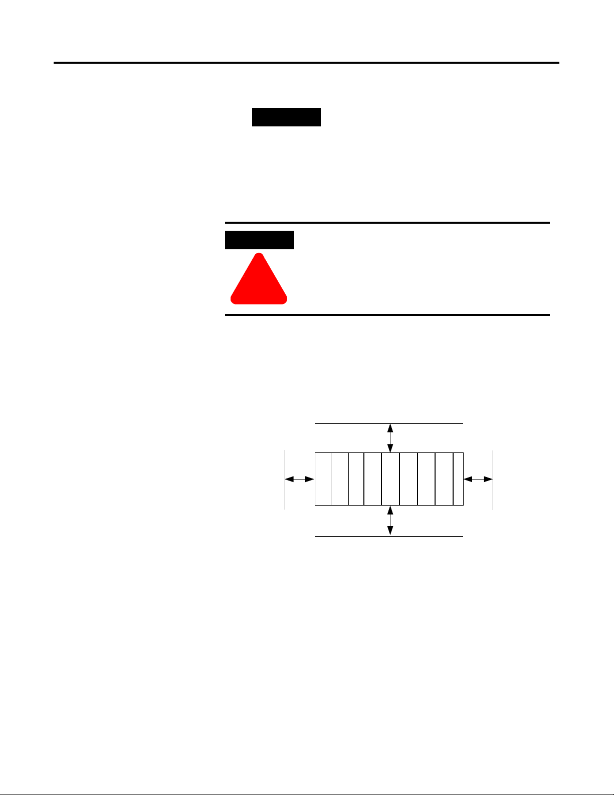
System Assembly. . . . . . . . . . . . . . . . . . . . . . . . . . . . . . . . 1-3
Mounting the Adapter and an I/O Module . . . . . . . . . . . . . 1-4
Minimum Spacing . . . . . . . . . . . . . . . . . . . . . . . . . . . . 1-4
Panel Mounting . . . . . . . . . . . . . . . . . . . . . . . . . . . . . . 1-4
Panel Mounting Procedure Using Modules as a Template 1-5
DIN Rail Mounting. . . . . . . . . . . . . . . . . . . . . . . . . . . . 1-6
Replacing the 1769-ADN within a System. . . . . . . . . . . . . . 1-6
Field Wiring Connections . . . . . . . . . . . . . . . . . . . . . . . . . 1-7
Grounding the Adapter . . . . . . . . . . . . . . . . . . . . . . . . 1-7
DeviceNet Wiring. . . . . . . . . . . . . . . . . . . . . . . . . . . . . 1-7
Setting the Network Address Switches . . . . . . . . . . . . . . . . 1-8
Configuring the 1769-ADN. . . . . . . . . . . . . . . . . . . . . . . . . 1-9
How Communication Takes Place
and I/O Image Table Mapping
Chapter 2
Communication Over the 1769 Bus . . . . . . . . . . . . . . . . . . 2-1
I/O Structure. . . . . . . . . . . . . . . . . . . . . . . . . . . . . . . . . . . 2-1
Adapter Status Words. . . . . . . . . . . . . . . . . . . . . . . . . . 2-2
Communication Choices . . . . . . . . . . . . . . . . . . . . . . . . . . 2-4
Mapping I/O Data into the Image Table. . . . . . . . . . . . . . . 2-4
1769-IA8I Individually Isolated 120V AC
Input Module (8 Point) . . . . . . . . . . . . . . . . . . . . . . . . . . . 2-5
Input Data. . . . . . . . . . . . . . . . . . . . . . . . . . . . . . . . . . 2-5
1769-IA16 120V ac Input Module (16 Point) . . . . . . . . . . . . 2-5
Input Data. . . . . . . . . . . . . . . . . . . . . . . . . . . . . . . . . . 2-5
1769-IF4 (Series A and B) Analog Current/Voltage
Input Module (4 Channel) . . . . . . . . . . . . . . . . . . . . . . . . . 2-6
Input Data. . . . . . . . . . . . . . . . . . . . . . . . . . . . . . . . . . 2-6
1769-IM12 240V AC Input Module (12 Point) . . . . . . . . . . . 2-6
Input Data. . . . . . . . . . . . . . . . . . . . . . . . . . . . . . . . . . 2-6
1769-IQ16 24V DC Sink/Source Input Module (16 Point) . . 2-6
Input Data. . . . . . . . . . . . . . . . . . . . . . . . . . . . . . . . . . 2-6
1769-OA8 100 to 240V AC Solid State
Output Module (8 Point) . . . . . . . . . . . . . . . . . . . . . . . . . . 2-7
Output Data . . . . . . . . . . . . . . . . . . . . . . . . . . . . . . . . 2-7
Input Data. . . . . . . . . . . . . . . . . . . . . . . . . . . . . . . . . . 2-7
i Publication 1769-UM001B-EN-P - October 2002
Page 6

ii
1769-OA16 100 to 240V AC Solid State
Output Module (16 Point) . . . . . . . . . . . . . . . . . . . . . . . . . 2-8
Output Data File . . . . . . . . . . . . . . . . . . . . . . . . . . . . . 2-8
Output Module’s Input Data File. . . . . . . . . . . . . . . . . . 2-8
1769-OB16 Solid State 24V DC Source
Output Module (16 Point) . . . . . . . . . . . . . . . . . . . . . . . . . 2-9
Output Data . . . . . . . . . . . . . . . . . . . . . . . . . . . . . . . . 2-9
Input Data. . . . . . . . . . . . . . . . . . . . . . . . . . . . . . . . . . 2-9
1769-OB16P Electronically Protected Solid-State 24V DC
Output Module . . . . . . . . . . . . . . . . . . . . . . . . . . . . . . . . . 2-10
Output Data . . . . . . . . . . . . . . . . . . . . . . . . . . . . . . . . 2-10
Input Data. . . . . . . . . . . . . . . . . . . . . . . . . . . . . . . . . . 2-10
1769-OF2 (Series A and B) Analog Current/Voltage
Output Module (2 Channel). . . . . . . . . . . . . . . . . . . . . . . . 2-11
Output Data . . . . . . . . . . . . . . . . . . . . . . . . . . . . . . . . 2-11
Input Data. . . . . . . . . . . . . . . . . . . . . . . . . . . . . . . . . . 2-11
1769-OV16 Solid State 24V DC Sink
Output Module (16 Point) . . . . . . . . . . . . . . . . . . . . . . . . . 2-12
Output Data . . . . . . . . . . . . . . . . . . . . . . . . . . . . . . . . 2-12
Input Data. . . . . . . . . . . . . . . . . . . . . . . . . . . . . . . . . . 2-12
1769-OW8 AC/DC Relay Output Module (8 Point) . . . . . . . 2-13
Output Data . . . . . . . . . . . . . . . . . . . . . . . . . . . . . . . . 2-13
Input Data. . . . . . . . . . . . . . . . . . . . . . . . . . . . . . . . . . 2-13
1769-OW8I Individually Isolated AC/DC Relay
Output Module (8 Point) . . . . . . . . . . . . . . . . . . . . . . . . . . 2-14
Output Data . . . . . . . . . . . . . . . . . . . . . . . . . . . . . . . . 2-14
Input Data. . . . . . . . . . . . . . . . . . . . . . . . . . . . . . . . . . 2-14
1769-OW16 AC/DC Relay Output Module (16 Point) . . . . . 2-15
Output Data File . . . . . . . . . . . . . . . . . . . . . . . . . . . . . 2-15
Output Module’s Input Data File. . . . . . . . . . . . . . . . . . 2-15
1769-IQ6XOW4 24V DC Sink/Source Input AC/DC Relay
Output Module (6 Point In, 4 Point Out) . . . . . . . . . . . . . . 2-16
Output Data . . . . . . . . . . . . . . . . . . . . . . . . . . . . . . . . 2-16
Input Data. . . . . . . . . . . . . . . . . . . . . . . . . . . . . . . . . . 2-16
1769-IT6 Thermocouple/mV Input Module. . . . . . . . . . . . . 2-17
Input Data. . . . . . . . . . . . . . . . . . . . . . . . . . . . . . . . . . 2-17
1769-IR6 RTD/Resistance Input Module . . . . . . . . . . . . . . . 2-18
Input Data. . . . . . . . . . . . . . . . . . . . . . . . . . . . . . . . . . 2-18
1769-IF4XOF2 Combination Analog Module . . . . . . . . . . . . 2-19
Input Data. . . . . . . . . . . . . . . . . . . . . . . . . . . . . . . . . . 2-19
Output Data . . . . . . . . . . . . . . . . . . . . . . . . . . . . . . . . 2-20
1769-HSC High-Speed Counter Module . . . . . . . . . . . . . . . 2-21
Output Array . . . . . . . . . . . . . . . . . . . . . . . . . . . . . . . . 2-21
Input Array . . . . . . . . . . . . . . . . . . . . . . . . . . . . . . . . . 2-22
Defaults . . . . . . . . . . . . . . . . . . . . . . . . . . . . . . . . . . . . . . 2-24
Publication 1769-UM001B-EN-P - October 2002
Page 7

Configuring Your Compact I/O
Series A DeviceNet Adapter
iii
Chapter 3
About RSNetworx . . . . . . . . . . . . . . . . . . . . . . . . . . . . . . . 3-1
Adding Your Series A DeviceNet Adapter Offline . . . . . . . . 3-1
Configuring Your Compact I/O System Offline. . . . . . . . . . 3-2
Configuring Your Series A Adapter . . . . . . . . . . . . . . . . 3-2
Using Banks of I/O . . . . . . . . . . . . . . . . . . . . . . . . . . . . . . 3-7
Configuration Rules for the Series A Adapter. . . . . . . . . 3-7
Configuring Discrete Input Modules. . . . . . . . . . . . . . . . . . 3-9
Configuring Discrete Output Modules . . . . . . . . . . . . . . . . 3-11
Configuring Analog Input Modules . . . . . . . . . . . . . . . . . . 3-14
Configuring Analog Output Modules . . . . . . . . . . . . . . . . . 3-17
Configuring Power Supplies, Cables, and End Cap . . . . . . . 3-20
Completing Configuration . . . . . . . . . . . . . . . . . . . . . . . . . 3-20
Auditing the Configuration . . . . . . . . . . . . . . . . . . . . . . 3-20
Viewing the Mapping Summaries . . . . . . . . . . . . . . . . . 3-20
Configuring Your Compact I/O System Online . . . . . . . . . . 3-21
Apply/OK Button. . . . . . . . . . . . . . . . . . . . . . . . . . . . . 3-21
Uploading Configurations. . . . . . . . . . . . . . . . . . . . . . . 3-23
Downloading Configurations . . . . . . . . . . . . . . . . . . . . 3-24
Using the Clear Memory Function. . . . . . . . . . . . . . . . . 3-25
Configured 1769-ADN Powerup Behavior . . . . . . . . . . . . . 3-25
Configuring Your Compact I/O
Series B DeviceNet Adapter
Chapter 4
About RSNetworx . . . . . . . . . . . . . . . . . . . . . . . . . . . . . . . 4-1
Adding Your Series B DeviceNet Adapter Offline . . . . . . . . 4-1
Configuring Your Compact I/O System Offline. . . . . . . . . . 4-2
Configuring Your Series B Adapter . . . . . . . . . . . . . . . . 4-2
Using Banks of I/O . . . . . . . . . . . . . . . . . . . . . . . . . . . . . . 4-6
Configuration Rules for Series B Adapters . . . . . . . . . . . 4-6
Configuring Discrete Input Modules. . . . . . . . . . . . . . . . . . 4-9
Configuring Discrete Output Modules . . . . . . . . . . . . . . . . 4-12
Configuring Analog Input Modules . . . . . . . . . . . . . . . . . . 4-17
Configuring Analog Output Modules . . . . . . . . . . . . . . . . . 4-21
Configuring Power Supplies, Cables, and End Cap . . . . . . . 4-25
Completing Configuration . . . . . . . . . . . . . . . . . . . . . . . . . 4-25
Auditing the Configuration . . . . . . . . . . . . . . . . . . . . . . 4-25
Viewing the Mapping Summaries . . . . . . . . . . . . . . . . . 4-26
Viewing the Transactions . . . . . . . . . . . . . . . . . . . . . . . 4-27
Configuring Your Compact I/O System Online . . . . . . . . . . 4-27
Apply/OK Button. . . . . . . . . . . . . . . . . . . . . . . . . . . . . 4-28
Uploading Configurations. . . . . . . . . . . . . . . . . . . . . . . 4-30
Downloading Configurations . . . . . . . . . . . . . . . . . . . . 4-31
Configuring Your Adapter for Quick Connect Operation. . . 4-32
Configured 1769-ADN Powerup Behavior . . . . . . . . . . . . . 4-33
Publication 1769-UM001B-EN-P - October 2002
Page 8

iv
Troubleshooting with the
Indicators
Application Examples
Chapter 5
Diagnostic Indicators. . . . . . . . . . . . . . . . . . . . . . . . . . . . . 5-1
Chapter 6
1747-SDN Application Example . . . . . . . . . . . . . . . . . . . . . 6-1
Hardware Setup. . . . . . . . . . . . . . . . . . . . . . . . . . . . . . 6-1
Configuring the SLC System . . . . . . . . . . . . . . . . . . . . . 6-1
Configuring the 1769-ADN DeviceNet Adapter . . . . . . . 6-2
Configuring the 1747-SDN . . . . . . . . . . . . . . . . . . . . . . . . . 6-6
Accessing the I/O Data from the 1769-ADN in the
SLC Processor . . . . . . . . . . . . . . . . . . . . . . . . . . . . . . . . . . 6-9
1756-DNB Application Example. . . . . . . . . . . . . . . . . . . . . 6-11
Hardware Setup. . . . . . . . . . . . . . . . . . . . . . . . . . . . . . 6-11
Configuring the Logix5550TM Controller System . . . . . . 6-12
Configuring the 1769-ADN DeviceNet Adapter . . . . . . . 6-12
Configuring the 1756-DNB. . . . . . . . . . . . . . . . . . . . . . . . . 6-16
Accessing the I/O Data from the 1769-ADN in the
Logix5550 Controller . . . . . . . . . . . . . . . . . . . . . . . . . . . . . 6-19
Specifications
Explicit Messaging Application
Examples
Appendix A
1769-ADN Specifications . . . . . . . . . . . . . . . . . . . . . . . . . . A-1
Series A Adapters General Specifications. . . . . . . . . . . . A-1
Series A Adapters Input/Output Specifications. . . . . . . . A-2
Series B Adapters Firmware General Specifications . . . . A-3
Series B Adapters Input/Output Specifications. . . . . . . . A-5
Appendix B
1756-DNB Explicit Messaging Application Example . . . . . . B-1
Get 1769-ADN Status . . . . . . . . . . . . . . . . . . . . . . . . . . B-1
Get 1769 I/O Module Status . . . . . . . . . . . . . . . . . . . . . B-4
Get 1769 I/O Module Configuration Size. . . . . . . . . . . . B-6
Set 1769 I/O Module Configuration. . . . . . . . . . . . . . . . B-8
Save 1769 I/O Module Configuration . . . . . . . . . . . . . B-11
Get 1769 I/O Module Configuration . . . . . . . . . . . . . . B-13
1747-SDN Explicit Messaging Application Example. . . . . . B-15
Get 1769-ADN Status . . . . . . . . . . . . . . . . . . . . . . . . . B-15
Get 1769 I/O Module Status . . . . . . . . . . . . . . . . . . . . B-18
Get 1769 I/O Module Configuration Size. . . . . . . . . . . B-22
Set 1769 I/O Module Configuration. . . . . . . . . . . . . . . B-23
Save 1769 I/O Module Configuration . . . . . . . . . . . . . B-27
Get 1769 I/O Module Configuration . . . . . . . . . . . . . . B-28
Ladder Logic Example Program . . . . . . . . . . . . . . . . . B-30
Discrete Module Configuration Files. . . . . . . . . . . . . . . . . B-31
Publication 1769-UM001B-EN-P - October 2002
Page 9

1769-ADN Throughput
Characteristics
Differences Between Series A and
B DeviceNet Adapters
v
Appendix C
Series A Adapters. . . . . . . . . . . . . . . . . . . . . . . . . . . . . C-1
About Adapter Throughput Characteristics . . . . . . . . . . . . . C-1
Turn-Around Time (ttat) . . . . . . . . . . . . . . . . . . . . . . . . . . C-1
Minimum Inter-Scan Delay (ISD) for Polled Connections . . C-2
Quick Connect Performance . . . . . . . . . . . . . . . . . . . . . . . C-3
Quick Connect Limitations . . . . . . . . . . . . . . . . . . . . . . C-4
Appendix D
About the Differences . . . . . . . . . . . . . . . . . . . . . . . . . . . . D-1
Publication 1769-UM001B-EN-P - October 2002
Page 10

vi
Notes:
Publication 1769-UM001B-EN-P - October 2002
Page 11

Preface
Read this preface to familiarize yourself with the rest of the manual.
This preface covers the following topics:
• who should use this manual
• how to use this manual
• related publications
• conventions used in this manual
• Allen-Bradley support
Who Should Use This
Manual
How to Use This Manual
Use this manual if you are responsible for designing, installing,
programming, or troubleshooting control systems that use
Allen-Bradley Compact I/O adapters.
As much as possible, we organized this manual to explain, in a
task-by-task manner, how to install, configure, program, operate, and
troubleshoot a control system using the 1769 I/O modules.
Manual Contents
If you want: See:
To install your DeviceNet adapter module Chapter 1
Information on how communication takes
place and on I/O image table mapping
To configure your Series A DeviceNet
adapter
To configure your Series B DeviceNet
adapter
Information on adapter diagnostics and
troubleshooting
Chapter 2
Chapter 3
Chapter 4
Chapter 5
Information on application examples Chapter 6
Specifications on the DeviceNet adapter Appendix A
Information on explicit messaging
application examples
Information on 1769-ADN throughput
characteristics
Information on the differences between
Series A and B DeviceNet adapters
1 Publication 1769-UM001B-EN-P - October 2002
Appendix B
Appendix C
Appendix D
Page 12

Preface 2
Related Documentation
The table below provides a listing of publications that contain
important information about Compact I/O products.
Title Publication
Number
MicroLogix 1500 System Overview 1764-SO001
CompactLogix Selection Guide 1769-SG001
Compact I/O Analog Modules User Manual 1769-UM002
1769-ADN Adapter User Manual 1769-UM001
Compact I/O 1769-ADN DeviceNet Adapter Module Installation
Instructions
Compact 1769-IQ6XOW4 24V dc Sink/Source Input AC/DC Relay
Output Module Installation Instructions
Compact 1769-OW8 AC/DC Relay Output Module Installation
Instructions
Compact 1769-OB16P 24V DC Installation Instructions 1769-IN004
Compact 1769-OW8I Individually Isolated AC/DC Relay Output
Module Installation Instructions
Compact 1769-OW16 16-Point ac/dc Relay Module Installation
Instructions
Compact 1769-IA16 120V ac Input Module Installation Instructions 1769-IN006
Compact 1769-IQ16 24V dc Sink/Source Input Module Installation
Instructions
Compact 1769-OB16 Solid State 24V dc Source Output Module
Installation Instructions
Compact 1769-OA8 100 to 240V ac Solid State Output Module
Installation Instructions
Compact 1769-OA16 100 to 240V ac Solid State Output Module
Installation Instructions
Compact 1769-OV16 Solid State 24V dc Sink Output Module
Installation Instructions
Compact 1769-IM12 240V ac Input Module Installation Instructions 1769-IN011
1769-IN001
1769-IN002
1769-IN003
1769-IN005
1769-IN062
1769-IN007
1769-IN008
1769-IN009
1769-IN061
1769-IN010
Publication 1769-UM001B-EN-P - October 2002
Compact 1769-IA8I Individually Isolated 120V ac Input Module
Installation Instructions
Compact 1769-HSC High Speed Counter Module Installation
Instructions
Compact 1769-HSC High Speed Counter Module User Manual 1769-UM006
Compact 1769-IF4XOF2 Combination Analog Module Installation
Instructions
Compact 1769-IF4XOF2 Combination Analog User Manual 1769-UM008
Compact 1769 Power Supplies Installation Instructions 1769-5.14
1769-IN012
1769-IN030
1769-IN057
Page 13

Preface 3
Title Publication
Number
Compact I/O Communication Bus Expansion Cables Installation
Instructions
Compact 1769-ECR Right End Cap/Terminator 1769-5.9
Compact 1769-ECL Left End Cap/Terminator 1769-5.16
Compact 1769-IF4 Analog Input Module Installation Instructions 1769-IN016
Compact 1769-OF2 Analog Output Module Installation Instructions 1769-IN017
1769-5.15
If you would like a manual, you can:
• download a free electronic version from the internet at
www.theautomationbookstore.com
• purchase a printed manual by:
– contacting your local distributor or Rockwell Automation
representative
– visiting www.theautomationbookstore.com and placing your
order
– calling 1.800.963.9548 (USA/Canada) or
001.330.725.1574 (Outside USA/Canada)
Conventions Used in This
Manual
The following conventions are used throughout this manual:
• Bulleted lists (like this one) provide information, not procedural
steps.
• Numbered lists provide sequential steps or hierarchical
information.
• Italic type is used for emphasis.
• Text in this font indicates words or phrases you should type.
Publication 1769-UM001B-EN-P - October 2002
Page 14

Preface 4
Allen-Bradley Support
Allen-Bradley offers support services worldwide, with over 75
Sales/Support Offices, 512 authorized distributors and 260 authorized
Systems Integrators located throughout the United States alone, plus
Allen-Bradley representatives in every major country in the world.
Local Product Support
Contact your local Allen-Bradley representative for:
• sales and order support
• product technical training
• warranty support
• support service agreement
Technical Product Assistance
If you need to contact Allen-Bradley for technical assistance, please
review the information in Chapter 4, Troubleshooting first. Then call
your local Allen-Bradley representative.
Your Questions or Comments on the Manual
If you find a problem with this manual, please notify us using the
self-mailer Publications Problem Report in the back of this manual.
If you have any suggestions for how this manual could be made more
useful to you, please contact us at the address below:
Rockwell Automation
Technical Communication Department
1 Allen-Bradley Drive
Mayfield Heights, OH 44124
Publication 1769-UM001B-EN-P - October 2002
Page 15
Chapter
Installing Your DeviceNet Adapter Module
This chapter explains how to install your DeviceNetTM adapter.
Included is information about:
• System Assembly
• Replacing the 1769-ADN within a System
• Field Wiring Connections
• Setting the Network Address Switches
1
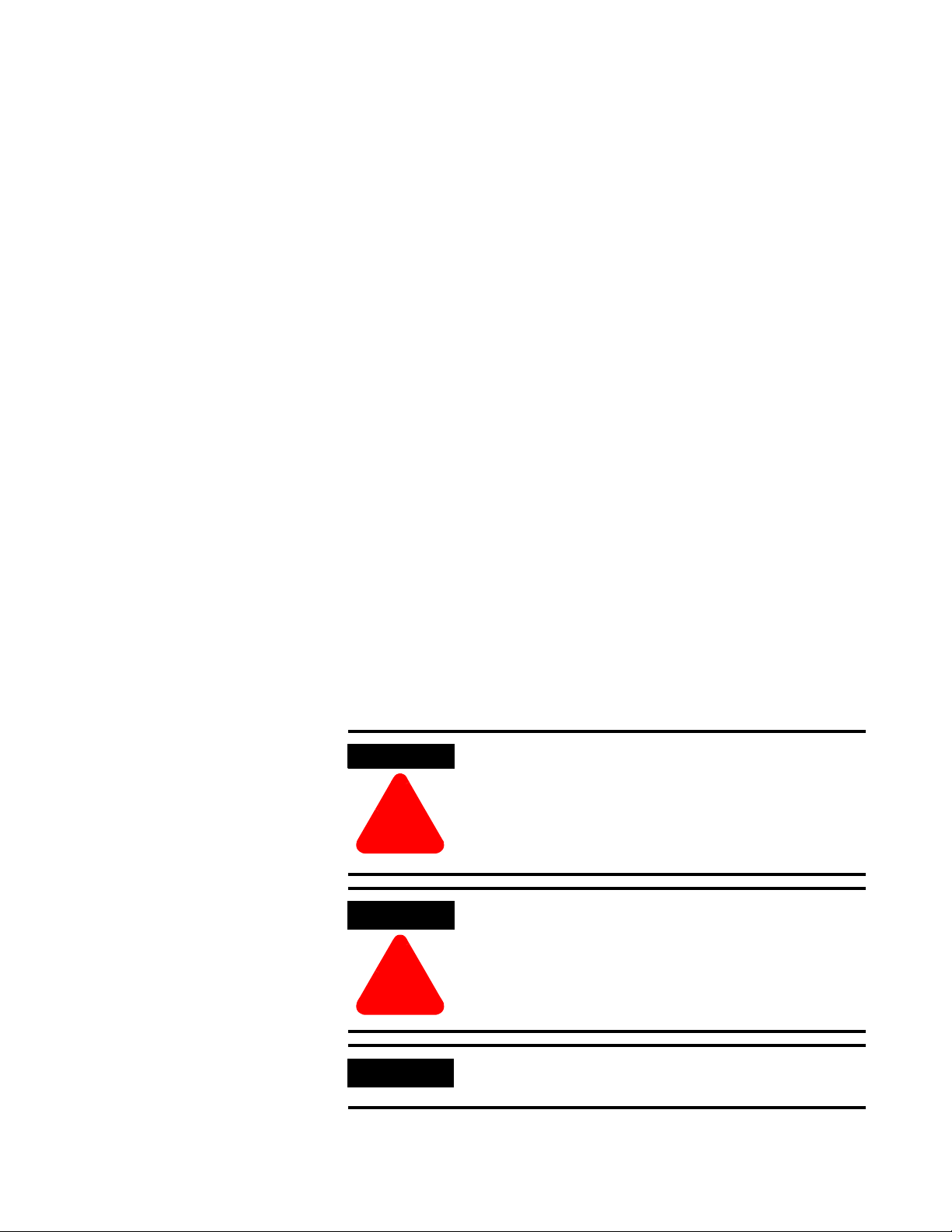
Compact I/O Module
Description
1a
MSIONS
DIAG
Comm Adapter
5
9
2
8a
8b
3
1b
6a
MSIONS
DIAG
Comm Adapter
4
7
6b
42125
Item Description Item Description
1a Upper panel mounting tab 6a Upper DIN-rail latch
1b Lower panel mounting tab 6b Lower DIN-rail latch
2 I/O diagnostic LEDs 7 Write-on label (user I.D. tag)
3 Module door with terminal
identification label
8a DeviceNet node address rotary
selection switches - Most
Significant Digit (MSD)
4 Stationary bus connector with male
pins
8b DeviceNet node address rotary
selection switches - Least
Significant Digit (LSD)
5 Nameplate label 9 Removable DeviceNet terminal
connector
1 Publication 1769-UM001B-EN-P - October 2002
Page 16
1-2 Installing Your DeviceNet Adapter Module
Module Installation
Compact I/O is suitable for use in an industrial environment when
installed in accordance with these instructions. Specifically, this
equipment is intended for use in clean, dry environments (Pollution
1
degree 2
60664-1).
1. Pollution Degree 2 is an environment where, normally, only non-conductive pollution occurs except that
occasionally a temporary conductivity caused by condensation shall be expected.
2. Over Voltage Category II is the load level section of the electrical distribution system. At this level transient
voltages are controlled and do not exceed the impulse voltage capability of the product’s insulation.
3. Pollution Degree 2 and Over Voltage Category II are International Electrotechnical Commission (IEC)
designations.
) and circuits not exceeding Over Voltage Category II2 (IEC
3
Prevent Electrostatic Discharge
ATTENTION
!
Electrostatic discharge can damage integrated
circuits or semiconductors if you touch bus
connector pins or the terminal block. Follow these
guidelines when you handle the module:
• Touch a grounded object to discharge static potential.
• Wear an approved wrist-strap grounding device.
• Do not touch the bus connector or connector pins.
• Do not touch circuit components inside the module.
• If available, use a static-safe work station.
• When not in use, keep the module in its static-shield box.
System Configuration
Remove Power
ATTENTION
Remove power before removing or inserting this
adapter. When you remove or insert an adapter
with power applied, an electrical arc may occur.
An electrical arc can cause personal injury or
property damage by:
!
• sending an erroneous signal to your system’s field devices,
causing unintended machine motion
• causing an explosion in a hazardous environment
Electrical arcing causes excessive wear to contacts
on both the module and its mating connector.
Worn contacts may create electrical resistance.
Refer to Using Banks of I/O on page 3-7 for system configuration
rules.
Publication 1769-UM001B-EN-P - October 2002
Page 17
Installing Your DeviceNet Adapter Module 1-3
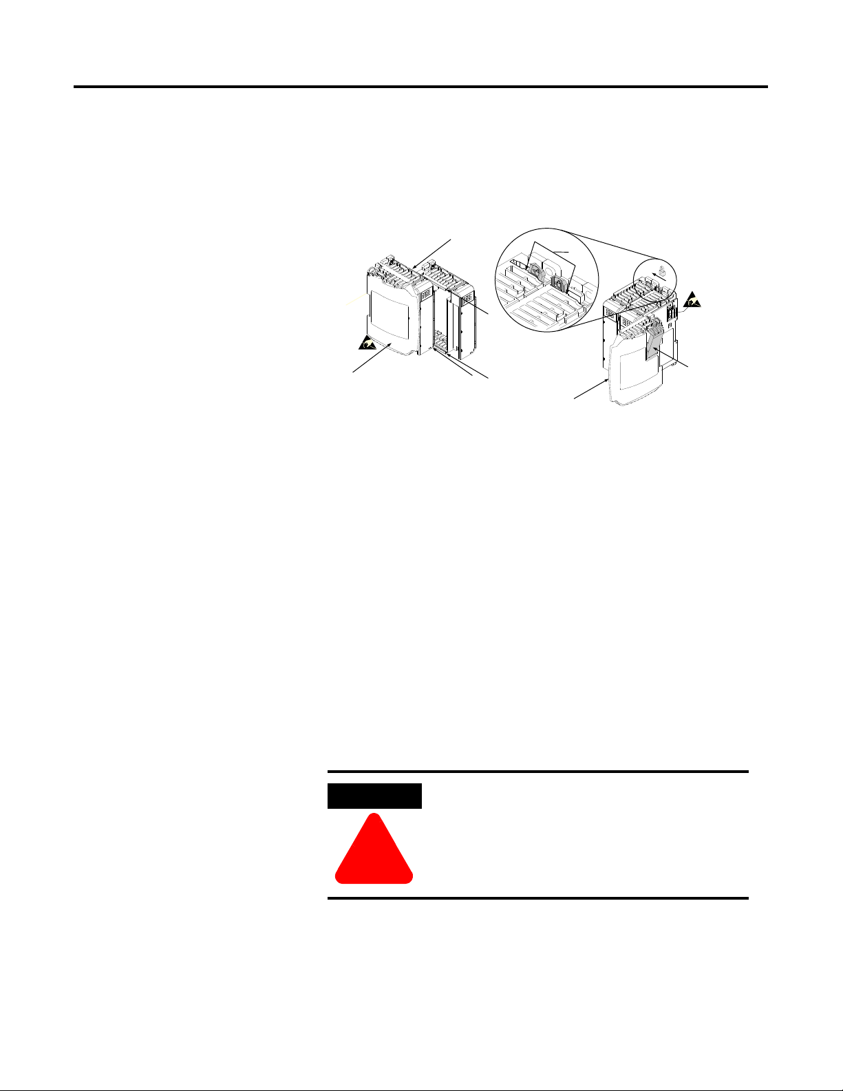
System Assembly
The adapter can be attached to adjacent 1769 modules before or after
mounting. For mounting instructions, see “Panel Mounting” on page
1-4, or “DIN Rail Mounting” on page 1-6. To work with a system that
is already mounted, see “Replacing the 1769-ADN within a System” on
page 1-6. The following procedure shows you how to assemble the
Compact I/O system.
a
b
c
a
1769-ADN
1. Disconnect power.
2. Check that the bus lever of the module to the right of the
1769-ADN is in the unlocked (fully right) position.
3. Use the upper and lower tongue-and-groove slots (a) to secure
the modules together.
a
a
d
e
42126
4. Move the module back along the tongue-and-groove slots until
the bus connectors line up with each other.
5. Push the bus lever of the module to the right of the 1769-ADN
back slightly to clear the positioning tab (b) using your fingers
or a small screwdriver.
6. To allow communication between the adapter and I/O modules,
move the bus lever of the module to the right of the 1769-ADN
fully to the left (c) until it clicks. Make sure it is locked firmly
into place.
ATTENTION
When attaching a 1769-ADN adapter, it is very
important that the bus connectors are securely
locked together to create a proper electrical
connection.
!
7. Attach an end cap terminator (d) to the last I/O module in the
system by using the tongue-and-groove slots as before.
Publication 1769-UM001B-EN-P - October 2002
Page 18
1-4 Installing Your DeviceNet Adapter Module
8. Lock the end cap bus terminator (e).
Mounting the Adapter and
an I/O Module
IMPORTANT
A 1769-ECR or 1769-ECL right or left end cap
must be used to terminate the end of the serial
communication bus.
9. Refer to the “DeviceNet Wiring” section on page 1-7.
ATTENTION
During panel or DIN rail mounting of all devices,
be sure that all debris (metal chips, wire strands,
etc.) is kept from falling into the adapter or
modules. Debris that falls into the adapter or
modules could cause damage on power up.
!
Minimum Spacing
Maintain spacing from enclosure walls, wireways, adjacent equipment,
etc. Allow 50mm (2in) of space on all sides for adequate ventilation,
as shown:
Top
1769 I/O
1769 I/O
Side Side
1769-ADN
1769 I/O
1769 I/O
1769 I/O
1769 Power Supply
Bottom
1769 I/O
End Cap or Cable
42124
Panel Mounting
Mount the adapter or module to a panel using two screws per adapter
or module. Use M4 or #8 panhead screws. Mounting screws are
required on every module.
Publication 1769-UM001B-EN-P - October 2002
Page 19
Installing Your DeviceNet Adapter Module 1-5
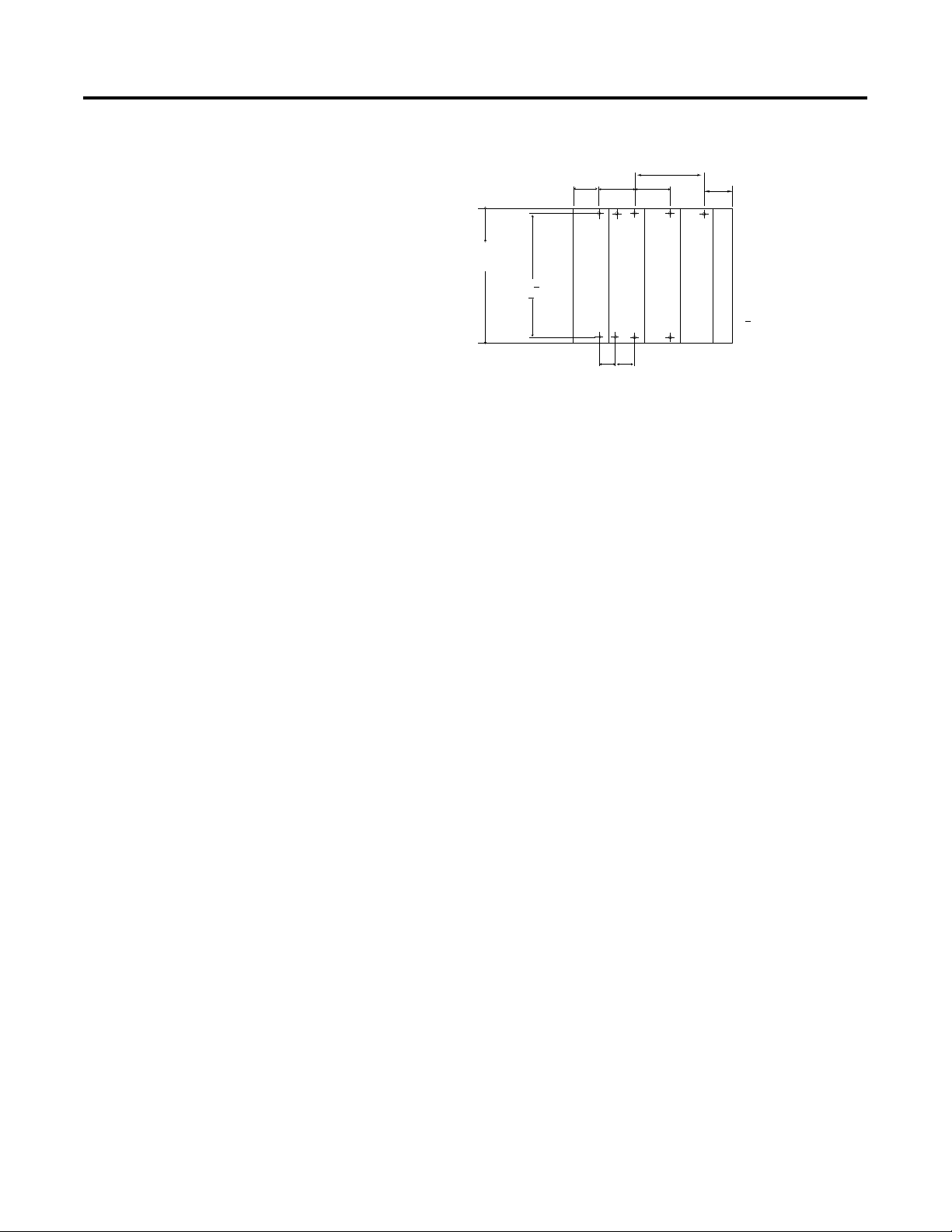
Panel Mounting Using the Dimensional Template
For more than 1 module: Number of modules x 35mm (1.38in)
70
40 35
(2.76)(1.58)
(1.38)
132
(5.197)
122.6+0.2
(4.826+
0.008)
1769-ADN
1769 Power Supply
28.5
(1.12)
1769 I/O
1769 I/O
Right End Cap
Hole spacing tolerance:
0.4mm (0.016in).
+
35
(1.38)
35
(1.38)
mm (in)
42121
Panel Mounting Procedure Using Modules as a Template
The following procedure allows you to use the assembled adapter and
modules as a template for drilling holes in the panel. If you have
sophisticated panel mounting equipment, you can use the
dimensional template provided on page 1-5.
Due to the module mounting hole tolerance, it is important to follow
these procedures:
1. On a clean work surface, assemble no more than three modules.
2. Using the assembled modules as a template, carefully mark the
center of all module-mounting holes on the panel.
3. Return the assembled modules to the clean work surface,
including any previously mounted modules.
4. Drill and tap the mounting holes for the recommended M4 or
#8 screw.
5. Place the modules back on the panel and check for proper hole
alignment.
6. Attach the modules to the panel using the mounting screws.
NOTE: If mounting more modules, mount only the last one of
this group and put the others aside. This reduces remounting
time during drilling and tapping of the next group.
7. Repeat steps 1 through 6 for any remaining modules.
Publication 1769-UM001B-EN-P - October 2002
Page 20

1-6 Installing Your DeviceNet Adapter Module
DIN Rail Mounting
The adapter can be mounted using the following DIN rails:
• 35 x 7.5mm (EN50022 - 35 x 7.5)
• 35 x 15mm (EN 50022 - 35 x 15)
Before mounting the module on a DIN rail, close the DIN rail latches.
Press the DIN rail mounting area of the module against the DIN rail.
The latches will momentarily open and lock into place.
Replacing the 1769-ADN
within a System
The adapter can be replaced while the system is mounted to a panel
(or DIN rail).
1. Remove power. See important note on page 1-2.
2. Remove the DeviceNet cable from the module by loosening the
upper and lower retaining screws of the DeviceNet connector
and removing the connector from the module.
3. Remove the upper and lower mounting screws from the adapter
(or open the DIN latches using a flat-blade or phillips-style
screwdriver).
4. On the right-side adjacent module, move its bus lever to the
right (unlock) to disconnect it from the adapter being removed.
5. Gently slide the disconnected adapter forward.
If you feel excessive resistance, make sure that you
disconnected the adapter from the bus and that you removed
both mounting screws (or opened the DIN latches).
Note: It may be necessary to rock the module slightly from front
to back to remove it, or, in a panel-mounted system, to loosen
the screws of adjacent modules.
Publication 1769-UM001B-EN-P - October 2002
6. Before installing the replacement adapter, be sure that the bus
lever on the right-side adjacent module is in the unlocked (fully
right) position.
7. Slide the replacement adapter into the open slot.
8. Connect the adapter and modules together by locking (fully left)
the bus lever on the right-side adjacent module.
9. Replace the mounting screws (or snap the adapter onto the DIN
rail).
Page 21
Installing Your DeviceNet Adapter Module 1-7
10. Replace the DeviceNet cable on the module by tightening the
upper and lower retaining screws and attaching the connector to
the module.
Set the network address switches to the same value as the removed
adapter.
Field Wiring Connections
Grounding the Adapter
This product is intended to be mounted to a well-grounded mounting
surface such as a metal panel. Additional grounding connections from
the adapter’s mounting tabs or metal DIN rail (if used), are not
required unless you cannot ground the mounting surface. Refer to
Industrial Automation Wiring and Grounding Guidelines, publication
1770-4.1, for additional information.
DeviceNet Wiring
MSIONS
DIAG
Comm Adapter
DeviceNet Connector 42123
1. Connect the DeviceNet cable to the removable connector as
shown.
Connect To
BLK Wire -V
BLU Wire CAN Low
Bare Wire Drain
WHT Wire CAN High
RED Wire +V
BLK
BLU
Bare
WHT
RED
Connector
42122
2. Insert the removable female connector into the mating male
connector on the DeviceNet adapter module.
3. Screw the removable connector to the adapter case with the
upper and lower mounting screws. Screw torque is 5-6 in-lbs.
Publication 1769-UM001B-EN-P - October 2002
Page 22
1-8 Installing Your DeviceNet Adapter Module
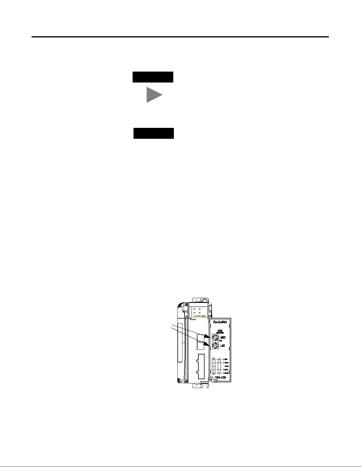
Setting the Network
Address Switches
TIP
DeviceNet cable colors are shown on the wiring
label on the front of the adapter.
Note: A 10-pin linear plug (i.e., 1787-PLUG10R) will
not fit while a 1799-DNETCON or -DNETSCON will
fit.
IMPORTANT
If the 1769-ADN is the last device connected to the
DeviceNet network trunkline, be sure to add or
move the termination resistor (Allen-Bradley part
number 1485A-C2 or a 120
Ω 5% or > ¼W resistor)
across the Blue (CAN Low) and White (CAN High)
wires. We recommend 121
Ω ¼W 1% metal film.
Set the network node address with the two rotary switches on the
front of the module. Use a small, slotted screwdriver to set the
switches. The switch labeled MSD (Most Significant Digit) sets the 10s
digit while the switch labeled LSD (Least Significant Digit) sets the 1s
digit.
Valid network node addresses are 00 through 63. Switch settings from
00 to 63 select network addresses 00 to 63. Switch settings from 64 to
99 instruct the adapter to use the software programmed value for the
node network address. (Address 95 is reserved and should not be
used for normal operation.)
Publication 1769-UM001B-EN-P - October 2002
TM
The software programmed value is set via RSNetworx
for DeviceNet
and stored in non-volatile memory on the 1769-ADN. The initial,
factory-preset setting of the software programmed value is 63.
MSIONS
DIAG
Comm Adapter
Address
Switches
Network
Address
Switches
42127
NOTE: The baud rate for the adapter is set by way of the module’s
automatic “auto baud” function at power-up.
Page 23

Installing Your DeviceNet Adapter Module 1-9
Use the removable, write-on label to mark your I.D. tag, etc. with
permanent ink. Your markings are visible when the module door is
closed.
Configuring the 1769-ADN
TIP
The 1769-ADN must be configured with RSNetworx for DeviceNet.
This configuration tool allows you to identify all of the devices (I/O
modules, power supplies, expansion cables, end caps) and their
locations in your 1769 system. The 1769-ADN must have the I/O
configuration loaded into its’ memory to perform the network
communication function.
The 1769-ADN will not accept I/O connections if the programmed
system configuration does not match the actual system configuration.
The 1769-ADN retains the programmed system configuration in
non-volatile memory so it can compare it with the actual system
configuration on power-up. For more information, refer to
Configuring Your Compact I/O Series A DeviceNet Adapter in Chapter 3
or Configuring Your Compact I/O Series B DeviceNet Adapter in
Chapter 4.
Series B adapters that have their node address
switches set to 95, startup in a special factory mode
that does not support I/O connections. Series B
adapters should not have their node address set to
95 for normal use.
Publication 1769-UM001B-EN-P - October 2002
Page 24

1-10 Installing Your DeviceNet Adapter Module
Notes:
Publication 1769-UM001B-EN-P - October 2002
Page 25

Chapter
2
How Communication Takes Place and I/O
Image Table Mapping
This chapter explains how communication takes place and about I/O
image table mapping. Included is information about:
• I/O Structure
• Communication Choices
• Mapping I/O Data into the Image Table
Communication Over the
1769 Bus
I/O Structure
One 1769-ADN DeviceNet adapter can interface with up to 30
Compact I/O modules to make a Compact I/O system. The adapter
communicates to other network system components (typically a
controller or scanner and/or programming terminals) over the
DeviceNet network.
The adapter communicates with its I/O modules over the 1769 bus.
The adapter and I/O modules also receive 5Vdc and 24V dc power
through the bus interface via a 1769 power supply. The 1769 bus and
all devices on the 1769 bus have system configuration limits. Refer to
Using Banks of I/O on page 3-7 for more information.
The I/O map for an I/O module is divided into input data words and
output data words. The number of input data words or output data
words can be 0 or more. The length of each I/O module’s input data
words or output data words vary in size, depending on the module’s
complexity. Each I/O module will support at least one input data
word or one output data word.
Output data is received by the adapter in the order of the installed I/O
modules. The output data for Slot 1 is received first, followed by the
output data for Slot 2, and so on up to Slot 30.
The amount of output data in the adapter’s output image for each I/O
module is based on the configuration of each I/O module done as
part of the 1769-ADN configuration. If an I/O module is configured to
have 0 words of output data, then it does not appear in the output
image of the 1769-ADN. Only a module’s output data can be in the
1769-ADN output image - a module’s configuration data cannot.
The first two words of input data sent by the adapter are the Adapter
Status Words. This is followed by the input data from each slot, in the
order of the installed I/O modules. The input data from Slot 1 is first
after the status words, followed by Input data from Slot 2, and so on
up to Slot 30.
1 Publication 1769-UM001B-EN-P - October 2002
Page 26
2-2 How Communication Takes Place and I/O Image Table Mapping
The amount of input data in the adapter’s input image for each I/O
module is based on the configuration of each I/O module done as
part of the 1769-ADN configuration. If an I/O module is configured to
have 0 words of input data, then it does not appear in the input image
of the 1769-ADN.
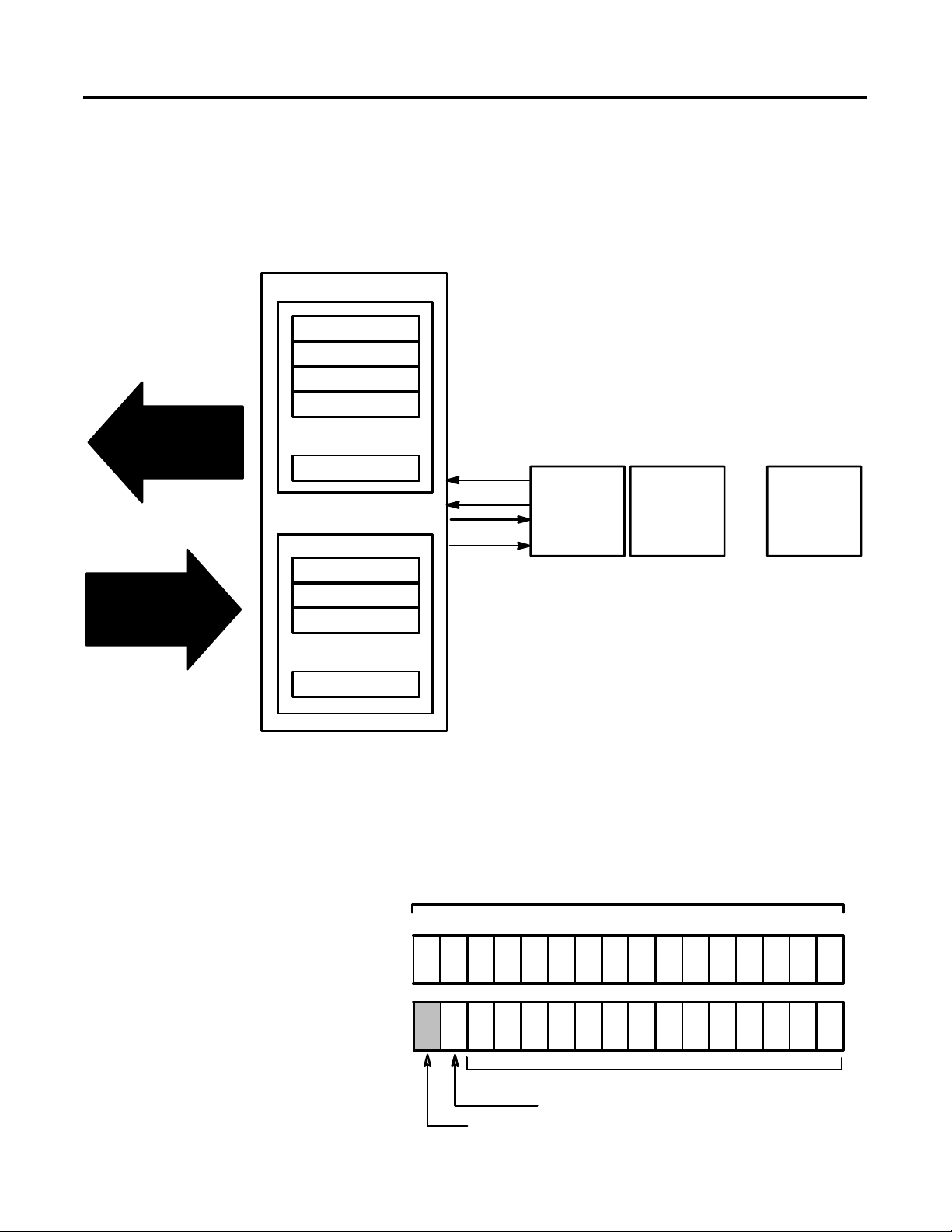
DeviceNet Adapter
Input Image (Read Data)
Adapter Status Words
Slot 1 Input Data
Slot 2 Input Data
Slot 3 Input Data
Network READ
Slot 30 Input Data
Output Image (Write Data)
...
Read
Write
I/O Module
Slot 1
I/O Module
Slot 2
I/O Module
...
Slot 30
Network WRITE
Slot 1 Output Data
Slot 2 Output Data
Slot 3 Output Data
...
Slot 30 Output Data
Adapter Status Words
The first two words (0 and 1) of the adapter input image contain the
adapter status. The adapter status consists of:
• I/O module data invalid bits - 1 status bit for each slot
• node address changed - 1 bit
Bit: 9 8 7 6 5 4 3 2 1 0
Word 0
Slot 16
Slot 15
Slot 14
Slot 13
Slot 12
I/O Module Data Invalid Bits
101112131415
Slot 8
Slot 9
Slot 10
Slot 11
24 23 22 21 20 19 18 17 16252627282930
42279
Slot 7
Slot 6
Slot 5
Slot 4
Slot 3
Slot 2
Slot 1
Publication 1769-UM001B-EN-P - October 2002
Word 1
Slot 30
NACB
Spare, not used
Slot 29
Node Address Changed Bit (NACB)
Slot 25
I/O Module Data Invalid Bits
Slot 26
Slot 27
Slot 28
Slot 24
Slot 23
Slot 22
Slot 21
Slot 20
Slot 19
Slot 18
Slot 17
42280
Page 27

How Communication Takes Place and I/O Image Table Mapping 2-3
The adapter status bit descriptions are shown in the following table.
Bit Description
I/O Module
Data Invalid
Is set (1) when
Word 0
Bit
I/O module data
is invalid for
slot position
01
Bit Description
Word 1
Bit
017
Is set (1) when
I/O module data
is invalid for
slot position
12 118
23 219
34 320
45 421
56 522
67 623
78 724
I/O Module
Data Invalid
89 825
910 926
10 11 10 27
11 12 11 28
12 13 12 29
13 14 13 30
14 15 Node Address
14
1
-
Changed
15 16 Not Used 15
2
-
1 This bit is set (1) when the node address switch setting
has been changed since powerup.
2 Not used - sent as zeroes.
Possible causes for an I/O Module Data Invalid are:
• transmission errors on the Compact I/O backplane
• a failed module
• incorrect module inserted in a slot position
• the configuration for an I/O module is invalid
The node address changed bit is set when the node address switch
setting has been changed since power up. The new node address
does not take affect until the adapter has been powered down and
then powered back up.
Publication 1769-UM001B-EN-P - October 2002
Page 28

2-4 How Communication Takes Place and I/O Image Table Mapping
Communication Choices
The Compact I/O DeviceNet adapter module supports multiple
communication choices. These choices all use the DeviceNet adapter
input image and output image structure previously described. The
DeviceNet master makes the actual communication choice. The
choices are:
1
Polled
- data is sent by the adapter in response to received data
Strobe - data is sent by the adapter in response to the strobe
command. The single bit allocated to the adapter in the strobe
message is not used. If the configured size of the input image (sent
from the adapter) is greater than 8 bytes, only the first 8 bytes of the
input image are returned (of which, the first 4 bytes, or 2 words, are
the adapter status words).
Change of State - data is sent by the adapter based on detection of
any changed value within the input data. Data is independently
received based on change of state from the sender. Data in both
directions can be acknowledged or unacknowledged depending on
the run time configuration of the system.
Cyclic - data is sent cyclically by the adapter based on a configured
time value. Data is independently received cyclically from the sender.
Data in both directions can be acknowledged or unacknowledged
depending on the run time configuration of the system.
Mapping I/O Data into the
Image Table
1769-IA8I Individually Isolated 120V AC Input Module (8 Point) 2-5
1769-IA16 120V ac Input Module (16 Point) (16 Point) 2-5
1769-IF4 (Series A and B) Analog Current/Voltage Input Module (4 Channel) 2-6
1769-IM12 240V AC Input Module (12 Point) 2-6
1769-IQ16 24V DC Sink/Source Input Module (16 Point) 2-6
1769-OA8 100 to 240V AC Solid State Output Module (8 Point) 2-7
1769-OA16 100 to 240V AC Solid State Output Module (16 Point) 2-8
1769-OB16 Solid State 24V DC Source Output Module (16 Point) 2-9
1769-OB16P Electronically Protected Solid-State 24V DC Output Module 2-10
1769-OF2 (Series A and B) Analog Current/Voltage Output Module (2 Channel) 2-11
1769-OV16 Solid State 24V DC Sink Output Module (16 Point) 2-12
1 Refer to Appendix C for some important system characteristics when using the polled mode (minimum
inter-scan delay I.D. for polled connections).
All Compact I/O modules are supported by the Series B DeviceNet
adapter. At present, these consist of:
Module Description For I/O data
definition, see:
Publication 1769-UM001B-EN-P - October 2002
Page 29
How Communication Takes Place and I/O Image Table Mapping 2-5
Module Description For I/O data
definition, see:
1769-OW8 AC/DC Relay Output Module (8 Point) 2-13
1769-OW8I Individually Isolated AC/DC Relay Output Module (8 Point) 2-14
1769-OW16 AC/DC Relay Output Module (16 Point) 2-15
1769-IQ6XOW4 24V DC Sink/Source Input AC/DC Relay Output Module (6 Point In, 4 Point Out) 2-16
1769-IT6 Thermocouple/mV Input Module 2-17
1769-IR6 RTD/Resistance Input Module 2-18
1769-IF4XOF2 Combination Analog Module 2-19
1769-HSC High-Speed Counter Module 2-21
1769-IA8I Individually
Isolated 120V AC Input
Module (8 Point)
IMPORTANT
The following sections, as referenced above, give the input and
output data definitions for each Compact I/O module type. Their
mapping into the adapter’s input and output images are dependent on
their slot number and configured input and output sizes (as defined in
the I/O Structure section on page 2-1).
These modules will only operate properly with
Series B DeviceNet adapters: 1769-OW16, -OA16,
-IF4XOF2, -HSC.
Input Data
For each 1769-IA8I input module, input data word 0 contains the
current state of the field input points. Bits 8 to 15 are not used.
Bit Position
1514131211109876543210
Word
0
0 0 0 0 0 0 0 0rrrrrrrr
r = read
1769-IA16 120V ac Input
Module (16 Point)
Input Data
For each 1769-IA16 input module, input data word 0 contains the
current state of the field input points.
Bit Position
1514131211109876543210
Word
0rrrrrrrrrrrrrrrr
r = read
Publication 1769-UM001B-EN-P - October 2002
Page 30
2-6 How Communication Takes Place and I/O Image Table Mapping
1769-IF4 (Series A and B)
Analog Current/Voltage
Input Module (4 Channel)
Input Data
For each 1769-IF4 input module, input data words 0-3 contain the
analog value of the inputs. Word 4 and 5 contain analog status and
error information.
Bit Position
15 14131211109876543210
Word
0 SGN Analog Input Data Channel 0
1 SGN Analog Input Data Channel 1
2 SGN Analog Input Data Channel 2
3 SGN Analog Input Data Channel 3
4 Not Used S3 S2 S1 S0
5 U0 O0U1O1U2O2U3O3 Set to 0
SGN= sign bit in two’s format
Sx = general status bit for channels 0 through 3. This bit is set (1) when an error (over- or
under-range) exists for that channel.
Ux = under-range flag bits for channels 0 through 3. These bits can be used in the control
program for error detection.
Ox = over-range flag bits for channels 0 through 3. These bits can be used in the control
program for error detection.
1769-IM12 240V AC Input
Module (12 Point)
1769-IQ16 24V DC
Sink/Source Input Module
(16 Point)
Input Data
For each 1769-IM12 input module, input data word 0 contains the
current state of the field input points. Bits 12 to 15 are not used.
Bit Position
1514131211109876543210
Word
0
0 0 0 0rrrrrrrrrrrr
r = read
Input Data
For each 1769-IQ16 input module, input data word 0 contains the
current state of the field input points.
Bit Position
1514131211109876543210
Word
0rrrrrrrrrrrrrrrr
Publication 1769-UM001B-EN-P - October 2002
r = read
Page 31

How Communication Takes Place and I/O Image Table Mapping 2-7
1769-OA8 100 to 240V AC
Solid State Output Module
(8 Point)
Output Data
For each 1769-OA8 module, output data word 0 contains the control
program’s directed state of the discrete output points. Bits 8 to 15 are
not used.
Bit Position
1514131211109876543210
Word
0
0 0 0 0 0 0 0 0 wwwwwwww
w = write
Input Data
For each 1769-OA8 module, input data word 0 contains the state of
the module’s output data (output data echo) word 0. During normal
operation (controller in Run), these input bits represent the logic state
that the outputs are directed to by the control program. They are also
dependent upon the:
• Program Mode (Hold Last or User-Defined Safe State)
configuration
• Fault Mode (Hold Last or User-Defined Safe State) configuration
For the 1769-OA8, input data word 0 bits 8 to 15 are not used.
Bit Position
1514131211109876543210
Word
0
0 0 0 0 0 0 0 0rrrrrrrr
r = read
IMPORTANT
The output module’s input data reflects the output
data echo of the module, not necessarily the
electrical state of the output terminals. It does not
reflect shorted or open outputs.
Publication 1769-UM001B-EN-P - October 2002
Page 32

2-8 How Communication Takes Place and I/O Image Table Mapping
1769-OA16 100 to 240V AC
Solid State Output Module
(16 Point)
Output Data File
Data output bits are turned on or off using the bit positions in Word 0.
1 = output on
0 = output off
Example: To turn on bit position 12, type 1 in Word 0, Bit 12.
For each module, slot x, word 0 in the output data file contains the
control program’s directed state of the discrete output points.
Bit Position
15 14 13 12 11 10 9 8 7 6 5 4 3 2 1 0
Word
0wwwwwwwwwwwwwwww
w = write
Output Module’s Input Data File
For each module, slot x, input data file word 0 contains the state of
the module’s output data (output data echo) file word 0. During
normal operation, these input bits represent the logic state that the
outputs are directed to by the control program. They are also
dependent upon the:
• Program Mode configuration (if supported by the controller)
• The Fault Mode configuration (if supported by the controller)
Bit Position
15 14 13 12 11 10 9 8 7 6 5 4 3 2 1 0
Word
0rrrrrrrrrrrrrrrr
r = read
IMPORTANT
The output module’s input data file reflects the
output data echo of the module, not necessarily the
electrical state of the output terminals. It does not
reflect shorted or open outputs.
It is important to use this input word if the controller
adapter supports the Program Mode or Fault Mode
function, and if it is configured to use them.
Publication 1769-UM001B-EN-P - October 2002
Page 33

How Communication Takes Place and I/O Image Table Mapping 2-9
1769-OB16 Solid State 24V
DC Source Output Module
(16 Point)
Output Data
For each 1769-OB16 module, output data word 0 contains the control
program’s directed state of the discrete output points.
Bit Position
1514131211109876543210
Word
0wwwwwwwwwwwwwwww
w = write
Input Data
For each 1769-OB16 module, input data word 0 contains the state of
the module’s output data (output data echo) word 0. During normal
operation (controller in Run), these input bits represent the logic state
that the outputs are directed to by the control program. They are also
dependent upon the:
• Program Mode (Hold Last or User-Defined Safe State)
configuration
• Fault Mode (Hold Last or User-Defined Safe State) configuration
Bit Position
1514131211109876543210
Word
0rrrrrrrrrrrrrrrr
r = read
IMPORTANT
The output module’s input data reflects the output
data echo of the module, not necessarily the
electrical state of the output terminals. It does not
reflect shorted or open outputs.
Publication 1769-UM001B-EN-P - October 2002
Page 34

2-10 How Communication Takes Place and I/O Image Table Mapping
1769-OB16P Electronically
Protected Solid-State 24V
DC Output Module
Output Data
For each 1769-OB16P module, output data word 0 contains the
control program’s directed state of the discrete output points.
Bit Position
1514131211109876543210
Word
0wwwwwwwwwwwwwwww
w = write
Input Data
For each 1769-OB16P module, input data word 0 contains the state of
the module’s output data (output data echo) word 0. During normal
operation (controller in Run), these input bits represent the logic state
that the outputs are directed to by the control program. They are also
dependent upon the:
• Program Mode (Hold Last or User-Defined Safe State)
configuration
• Fault Mode (Hold Last or User-Defined Safe State) configuration
Bit Position
1514131211109876543210
Word
0rrrrrrrrrrrrrrrr
r = read
IMPORTANT
The output module’s input data reflects the output
data echo of the module, not necessarily the
electrical state of the output terminals. It does not
reflect shorted or open outputs.
Publication 1769-UM001B-EN-P - October 2002
Page 35

How Communication Takes Place and I/O Image Table Mapping 2-11
1769-OF2 (Series A and B)
Analog Current/Voltage
Output Module (2 Channel)
Output Data
For each 1769-OF2 module, output data words 0 and 1 contain the
channel 0 and channel 1 output data.
Bit Position
15 14131211109876543210
Word
0 SGN Analog Output Data Channel 0
1 SGN Analog Output Data Channel 1
SGN= sign bit in two’s compliment format
Input Data
For each 1769-OF2 module, input data words 0-1 contain analog
status and error information. Input data words 2-3 contain the state of
the module’s output data (output data echo) words 0-1. During
normal operation (controller in Run), these input words represent the
analog values that the outputs are directed to by the control program.
They are also dependent upon the:
• Program Mode configuration (Hold Last or User-Defined Safe
State)
• Fault Mode configuration (Hold Last or User-Defined Safe State)
Bit Position
15 14131211109876543210
Word
0 D0 H0 D1 H1 Not Used (Bits set to 0) S1 S0
1 U0 O0U1O1 Bits set to 0
2 SGN Output Data Loopback/Echo Channel 0
3 SGN Output Data Loopback/Echo Channel 1
SGN= sign bit in two’s format
Sx = general status bits. When set, these bits indicate an error (over-range, under-range, or
diagnostic bit) associated with that channel or a module hardware error.
Ux = under-range flag bits
Ox = over-range flag bits
Dx = diagnostic bits. When set, they indicate a broken output wire or high load resistance
(not used on voltage outputs).
Hx = hold last state bits. When set, they indicate that the channel is in a hold last state condition.
IMPORTANT
The output module’s input data reflects the analog
output data echo of the module, not necessarily the
electrical state of the output terminals. It does not
reflect shorted or open outputs.
Publication 1769-UM001B-EN-P - October 2002
Page 36
2-12 How Communication Takes Place and I/O Image Table Mapping
1769-OV16 Solid State 24V
DC Sink Output Module
(16 Point)
Output Data
For each 1769-OV16 module, output data word 0 contains the control
program’s directed state of the discrete output points.
Bit Position
1514131211109876543210
Word
0wwwwwwwwwwwwwwww
w = write
Input Data
For each 1769-OV16 module, input data word 0 contains the state of
the module’s output data (output data echo) word 0. During normal
operation (controller in Run), these input bits represent the logic state
that the outputs are directed to by the control program. They are also
dependent upon the:
• Program Mode configuration (Hold Last or User-Defined Safe
State)
• Fault Mode configuration (Hold Last or User-Defined Safe State)
Bit Position
1514131211109876543210
Word
0rrrrrrrrrrrrrrrr
r = read
IMPORTANT
The output module’s input data reflects the output
data echo of the module, not necessarily the
electrical state of the output terminals. It does not
reflect shorted or open outputs.
Publication 1769-UM001B-EN-P - October 2002
Page 37

How Communication Takes Place and I/O Image Table Mapping 2-13
1769-OW8 AC/DC Relay
Output Module (8 Point)
Output Data
For each 1769-OW8 module, output data word 0 contains the control
program’s directed state of the discrete output points. Bits 8 to 15 are
not used.
Bit Position
1514131211109876543210
Word
0
0 0 0 0 0 0 0 0 wwwwwwww
w = write
Input Data
For each 1769-OW8 module, input data word 0 contains the state of
the module’s output data (output data echo). During normal operation
(controller in Run), these input bits represent the logic state that the
outputs are directed to by the control program. They are also
dependent upon the:
• Program Mode configuration (Hold Last or User-Defined Safe
State)
• Fault Mode configuration (Hold Last or User-Defined Safe State)
For the 1769-OW8, input data word 0 bits 8 to 15 are not used.
Bit Position
1514131211109876543210
Word
0
0 0 0 0 0 0 0 0rrrrrrrr
r = read
IMPORTANT
The output module’s input data reflects the output
data echo of the module, not necessarily the
electrical state of the output terminals. It does not
reflect shorted or open outputs.
Publication 1769-UM001B-EN-P - October 2002
Page 38

2-14 How Communication Takes Place and I/O Image Table Mapping
1769-OW8I Individually
Isolated AC/DC Relay
Output Module (8 Point)
Output Data
For each 1769-OW8I module, output data word 0 contains the control
program’s directed state of the discrete output points. Bits 8 to 15 are
not used.
Bit Position
1514131211109876543210
Word
0
0 0 0 0 0 0 0 0 wwwwwwww
w = write
Input Data
For each 1769-OW8I module, input data word 0 contains the state of
the module’s output data (output data echo). During normal operation
(controller in Run), these input bits represent the logic state that the
outputs are directed to by the control program. They are also
dependent upon the:
• Program Mode configuration (Hold Last or User-Defined Safe
State)
• Fault Mode configuration (Hold Last or User-Defined Safe State)
For the 1769-OW8I, input data word 0 bits 8 to 15 are not used.
Bit Position
1514131211109876543210
Word
0
0 0 0 0 0 0 0 0rrrrrrrr
r = read
IMPORTANT
The output module’s input data reflects the output
data echo of the module, not necessarily the
electrical state of the output terminals. It does not
reflect shorted or open outputs.
Publication 1769-UM001B-EN-P - October 2002
Page 39

How Communication Takes Place and I/O Image Table Mapping 2-15
1769-OW16 AC/DC Relay
Output Module (16 Point)
Output Data File
Data output bits are turned on or off using the bit positions in Word 0.
1 = output on
0 = output off
Example: To turn on bit position 12, type 1 in Word 0, Bit 12.
For each module, slot x, word 0 in the output data file contains the
control program’s directed state of the discrete output points.
Bit Position
1514131211109876543210
Word
0wwwwwwwwwwwwwwww
w = write only
Output Module’s Input Data File
For each module, slot x, input data file word 0 contains the state of
the module’s output data (output data echo) file word 0. During
normal operation, these input bits represent the logic state that the
outputs are directed to by the control program. They are also
dependent upon the:
• Program Mode configuration (if supported by the controller)
• The Fault Mode configuration (if supported by the controller).
Bit Position
1514131211109876543210
Word
0rrrrrrrrrrrrrrrr
r = read only
IMPORTANT
The output module’s input data file reflects the
output data echo of the module, not necessarily the
electrical state of the output terminals. It does not
reflect shorted or open outputs.
It is important to use this input word if the controller
adapter supports the Program Mode or Fault Mode
function, and if it is configured to use them.
Publication 1769-UM001B-EN-P - October 2002
Page 40

2-16 How Communication Takes Place and I/O Image Table Mapping
1769-IQ6XOW4 24V DC
Sink/Source Input AC/DC
Relay Output Module
(6 Point In, 4 Point Out)
Output Data
For each 1769-IQ6XOW4 module, output data word 0 contains the
control program’s directed state of the discrete output points. Bits 4 to
15 are not used.
Bit Position
1514131211109876543210
Word
0
0 0 0 0 0 0 0 0 0 0 0 0 wwww
w = write
Input Data
For each 1769-IQ6XOW4 module, input data word 0 contains the
current state of the field input points. Input data word 1 contains the
state of the module’s output data (output data echo). During normal
operation (controller in Run), these input bits represent the logic state
that the outputs are directed to by the control program. They are also
dependent upon the:
• Program Mode configuration (Hold Last or User-Defined Safe
State)
• Fault Mode configuration (Hold Last or User-Defined Safe State)
For the 1769-IQ6XOW4, input data word 0 bits 6 to 15 are not used.
Bit Position
1514131211109876543210
Word
0 0 0 0 0 0 0 0 0 0rrrrrr
1
0 0 0 0 0 0 0 0 0 0 0 0rrrroutput
r = read
IMPORTANT
Input data word 1 reflects the output data echo of
the module, not necessarily the electrical state of the
output terminals. It does not reflect shorted or open
outputs.
real
inputs0
data
echo
Publication 1769-UM001B-EN-P - October 2002
Page 41

How Communication Takes Place and I/O Image Table Mapping 2-17
1769-IT6 Thermocouple/mV
Input Module
Input Data
The input data file contains the analog values of the inputs.
Bit Position
151413121110 9 8 76543210
Word
0 Analog Input Data Channel 0
1 Analog Input Data Channel 1
2 Analog Input Data Channel 2
3 Analog Input Data Channel 3
4 Analog Input Data Channel 4
5 Analog Input Data Channel 5
6OC7OC6OC5OC4OC3OC2OC1OC0S7S6S5S4S3S2S1S0
7U0O0U1U0U2O2U3O3U4O4U5O5U6O6U7O7
Sx = General status bit for channels 0-5 and CJC sensors (S6 and S7). This bit is set (1) when an error
(over-range, under-range, open-circuit, or input data not valid) exists for that channel. An input data not valid
condition is determined by the user program. This condition occurs when the first analog-to-digital conversion
is still in progress, after a new configuration has been sent to the module. Refer to the Compact
Thermocouple/mV Input Module User Manual, publication 1769-UM004A-EN-P for additional details.
OCx = Open circuit detection bits indicate an open input circuit on channels 0-5 (OC0 - OC5) and on CJC sensors
CJC0 (OC6) and CJC1 (OC7). The bit is set (1) when an open-circuit condition exists.
Ux = Under-range flag bits for channels 0-5 and the CJC sensors (U6 and U7). For thermocouple inputs, the
under-range bit is set (1) when a temperature measurement is below the normal operating range for a given
thermocouple type. For millivolt inputs, the under-range bit indicates a voltage that is below the normal
operating range. These bits can be used in the control program for error detection. The bits are reset (0) by the
module when within the normal operating range.
Ox = Over-range flag bits for channels 0-5 and the CJC sensors (O6 and O7). For thermocouple inputs, the
over-range bit is set (1) when a temperature measurement is above the normal operating range for a given
thermocouple type. For millivolt inputs, the over-range bit indicates a voltage that is above the normal
operating range. These bits can be used in the control program for error detection.
™ I/O
Publication 1769-UM001B-EN-P - October 2002
Page 42

2-18 How Communication Takes Place and I/O Image Table Mapping
1769-IR6 RTD/Resistance
Input Module
Input Data
The first six words (0 to 5) of the input data file contain the analog
RTD or resistance values of the inputs. Words 6 and 7 provide
sensor/channel status feedback for use in your control program as
shown below.
Bit Position
151413121110 9 8 76543210
Word
0 RTD/Resistance Input Data Channel 0
1 RTD/Resistance Input Data Channel 1
2 RTD/Resistance Input Data Channel 2
3 RTD/Resistance Input Data Channel 3
4 RTD/Resistance Input Data Channel 4
5 RTD/Resistance Input Data Channel 5
6 Not Used OC5 OC4 OC3 OC2 OC1 OC0 Not
Used
7U0O0U1O1U2O2U3O3U4O4U5O5 Not Used
Sx = General status bit for channels 0-5. This bit is set (1) when an error (over-range, under-range, open-circuit,
or input data not valid) exists for that channel. An input data not valid condition is determined by the user
program. This condition occurs when the first analog-to-digital conversion is still in progress, after a new
configuration has been sent to the module. Refer to the Compact
Manual, publication 1769-UM005A-EN-P for additional details.
OCx = Open circuit detection bits indicate an open input circuit on channels 0-5 (OC0 - OC5). The bit is set (1)
when either an open or shorted input for RTD inputs or an open input for resistance inputs is detected.
Short-circuit detection for resistance inputs is not indicated because 0 is a valid number.
Ux = Under-range flag bits for channels 0-5, using RTD inputs only. These bits can be used in the control
program for error detection. There is no under-range error for a direct resistance input, because 0 is a valid
number.
Ox = Over-range flag bits for channels 0-5, using either RTD or resistance inputs. These bits can be used in the
control program for error detection.
™ I/O RTD/Resistance Input Module User
S5 S4 S3 S2 S1 S0
Publication 1769-UM001B-EN-P - October 2002
Page 43

How Communication Takes Place and I/O Image Table Mapping 2-19
1769-IF4XOF2 Combination
Analog Module
0 SGN Analog Input Data Channel 0 0000000
1 SGN Analog Input Data Channel 1 0000000
2 SGN Analog Input Data Channel 2 0000000
Input Data
The input data file provides access to input data for use in the control
program, over-range indication for the input and output channels, and
output data feedback as described below.
IMPORTANT
15 14 131211109876543210
Word
Input words 6 and 7 contain the Output Data
Echo/Loopback information for output channels 0
and 1 respectively. Bits 0 through 6 and bit 15 or
words 6 and 7 should always be set to zero in your
control program. If they are not set to 0, the invalid
data flag (Ex) will be set for that channel by the
module. However, the channel will continue to
operate with the previously converted value.
Bit Position
3 SGN Analog Input Data Channel 3 0000000
4 Not Used
5Not
Used
H0 Not
Used
H1 Not Used
1
1
I3 I2 I1 I0
E1 E0 O1 O0
6 SGN Output Data Echo/Loopback for Output Channel 0 0000000
7 SGN Output Data Echo/Loopback for Output Channel 1 0000000
1 All unused bits are set to 0 by the module.
SGN = Sign bit in two’s complement format. Always positive (equal to zero) for the 1769-IF4XOF2 module.
Ix = Over-range flag bits for input channels 0 through 3. These bits can be used in the control program for error
detection. When set to 1, the bits signal that the input signal is outside the normal operating range. However, the
module continues to convert analog data to the maximum full-range value. When the over-range condition is cleared,
the bits are automatically reset (0).
Ox = Word 5, bits 0 and 1, provide over-range indication for output channels 0 and 1. These bits can be used in the
control program for error detection. When set to 1, the bits signal that the output signal is outside the normal
operating range. However, the module continues to convert analog data to the maximum full-range value. When the
over-range condition is cleared, the bits are automatically reset (0). Under-range indication is not provided
because zero is a valid number.
Ex = When set (1), this bit indicates that invalid data (e.g. the value sent by the controller is outside the standard
output range or increment; e.g. 128, 256, etc.) has been set in the output data bits 0 through 6, or the sign bit (15).
Hx = Hold Last State bits. When set (1), these bits indicate that the channel is in a Hold Last State condition.
Words 6 and 7 = These words reflect the analog output data echo of the analog value being converted by the
digital/analog converter, not necessarily the electrical state of the output terminals. They do not reflect shorted or
open outputs.
It is only important to use the loopback function of input words 6 and 7 if the controller supports the
Program Mode or Fault Mode functions, and if it is configured to use them.
Publication 1769-UM001B-EN-P - October 2002
Page 44

2-20 How Communication Takes Place and I/O Image Table Mapping
Output Data
The output data file applies only to output data from the module as
shown in the table below.
IMPORTANT
Bits 0 through 6 and bit 15 of output data words 0
and 1 should always be set to zero in your control
program. If they are not set to 0, the invalid data flag
(Ex) will be set for that channel. However, the
channel will continue to operate with the previously
converted value. If a MVM (Move with Mask)
instruction is used with a mask of 7F80 (hexidecimal)
to move data to the output words, writing to bits 0
through 6 and bit 15 can be avoided.
Bit Position
1514131211109876543210
Word
0 SGN Analog Output Data Channel 0 0000000
1 SGN Analog Output Data Channel 1 0000000
SGN = Sign bit in two’s complement format. Always positive (equal to zero) for the 1769-IF4XOF2
module.
Publication 1769-UM001B-EN-P - October 2002
Page 45

How Communication Takes Place and I/O Image Table Mapping 2-21
1769-HSC High-Speed
Counter Module
Output Array
The Output Array, which consists of 34 words, allows you to access
the module’s real-time output data to control the module. The
default value is all zeros.
IMPORTANT
IMPORTANT
The Output Array contains dynamic configuration
data. The settings in the Output Array must be
compatible with the settings in the Configuration
Array.
For example, do not attempt to set Counter Control
Bits for a given counter in the Output Array unless
NumberOfCounters in the Configuration Array
indicates that the counter is declared to be used.
All Not Used bits (shaded in the table below) must be
set to 0 or the InvalidOutput bit in the Input Array
will be set. When the InvalidOutput bit is set, the
entire Output Array is rejected until an Output Array
that does not have this error is sent.
Word
0 Out 15Out 14Out 13Out 12Out 11Out 10Out9Out8Out7Out6Out5Out4Out3Out2Out1Out
1 Out 15Out 14Out 13Out 12Out 11Out 10Out9Out8Out7Out6Out5Out4Out3Out2Out1Out
2 R15 R14 R13 R12 R11 R10 R9 R8 R7 R6 R5 R4 R3 R2 R1 R0 Range Enable
3
4 Not Used RBF Not Used Reset Blown Fuse
5 Not Used RPW RREZ Z Inh Z Inv D Inh D Inv RU RO SP En Counter 0 Control Bits
6
7 Not Used RPW Not Used D Inv RU RO SP En Counter 2 Control Bits
8 Not Used RPW Not Used D Inv RU RO SP En Counter 3 Control Bits
9
10
11
12
13
14 Range12To15[0].OutputControl Range Output Control
15
16
17
18
19
15 14 13 12 11 10 09 08 07 06 05 04 03 02 01 00
Not Used RPW RREZ Z Inh Z Inv D Inh D Inv RU RO SP En Counter 1 Control Bits
Range12To15[0].HiLimOrDirWr
Range12To15[0].LowLimit Range Low Limit
Not Used Inv Not Used LDW Type Not Used ToThisCtr
Range12To15[1].HiLimOrDirWr
Range12To15[1].LowLimit Range Low Limit
Bit
Output On Mask
0
Output Off Mask
0
Not Used Not Used
Not Used Not Used
Range High Limit or
Direct Write Value
Range Configuration
Flags
Range High Limit or
Direct Write Value
Function
Publication 1769-UM001B-EN-P - October 2002
Page 46

2-22 How Communication Takes Place and I/O Image Table Mapping
Word
20 Range12To15[1].OutputControl Range Output Control
21
22
23
24
25
26 Range12To15[2].OutputControl Range Output Control
27
28
29
30
31
32 Range12To15[3].OutputControl Range Output Control
33
15 14 13 12 11 10 09 08 07 06 05 04 03 02 01 00
Not Used Inv Not Used LDW Type Not Used ToThisCtr
Range12To15[2].HiLimOrDirWr
Range12To15[2].LowLimit Range Low Limit
Not Used Inv Not Used LDW Type Not Used ToThisCtr
Range12To15[3].HiLimOrDirWr
Range12To15[3].LowLimit Range Low Limit
Not Used Inv Not Used LDW Type Not Used ToThisCtr
Bit
Function
Range Configuration
Flags
Range High Limit or
Direct Write Value
Range Configuration
Flags
Range High Limit or
Direct Write Value
Range Configuration
Flags
Input Array
The Input Array, which consists of 35 words, allows read-only access
to the module’s input data via word and bit access.The Input Array is
described below. The functions are described in more detail in the
sections following the table.
IMPORTANT
During the non-run states (program and fault), the
module continues to update the Input Array
(continues counting, etc). Depending on the bus
master, you may not see this.
TIP
Status bits for a particular counter reflect the
configuration settings for that counter. To receive
valid status, the counter must be enabled and the
module must have stored a valid configuration for
that counter.
Gen
Error
Bit
Invalid
Output
Mod
Config
Not Used
Out0Overcurrent through
Out3Overcurrent
Status Flags
Word
0
1 Readback.0 through Readback.15 Readback
2
15 14 13 12 11 10 09 08 07 06 05 04 03 02 01 00
Not Used Z1 B1 A1 Z0 B0 A0 Input State
InvalidRangeLimit12
through
InvalidRangeLimit15
InvalidCtrAssignToRange12
through
InvalidCtrAssignToRange15
Function
Publication 1769-UM001B-EN-P - October 2002
Page 47

How Communication Takes Place and I/O Image Table Mapping 2-23
Word
15 14 13 12 11 10 09 08 07 06 05 04 03 02 01 00
Function
3 RangeActive.0 through RangeActive.15 Range Active
Bit
4
5
6
7
8
9
10
11
12
13
14
15
16
17
18
19
20
21
22
Not Used C0PW RV Not Used IDW REZ CUdf COvf Counter 0 Status Flags
Not Used C1PW RV IC IDW REZ CUdf COvf Counter 1 Status Flags
Ctr[0].CurrentCount Counter 0 Current Count
Ctr[0].StoredCount Counter 0 Stored Count
Ctr[0].CurrentRate Counter 0 Current Rate
Ctr[0].PulseInterval Counter 0 Pulse Interval
Not Used Not Used
Ctr[1].CurrentCount Counter 1 Current Count
Ctr[1].StoredCount Counter 1 Stored Count
Ctr[1].CurrentRate Counter 1 Current Rate
Ctr[1].PulseInterval Counter 1 Pulse Interval
23 Not Used Not Used
24
25
26
27
28
29
30
31
32
33
34
Not Used C2PW RV IC IDW
Not Used C3PW RV IC IDW
Ctr[2].CurrentCount Counter 2 Current Count
Ctr[2].CurrentRate Counter 2 Current Rate
Not
Used
CUdf COvf
Counter 2 Status Flags
Not Used Not Used
Ctr[3].CurrentCount Counter 3 Current Count
Ctr[3].CurrentRate Counter 3 Current Rate
Not
Used
CUdf COvf
Counter 3 Status Flags
Publication 1769-UM001B-EN-P - October 2002
Page 48

2-24 How Communication Takes Place and I/O Image Table Mapping
Defaults
Factory defaults are the values assigned when you:
• first power up the system, and
• no previous user-programmed stored settings have been applied
Each I/O module has default values associated with it.
Module defaults for I/O size: Factory defaults
(words)
Description Input Output Input Output
1769-IA8I Individually Isolated 120V
AC Input Module (8 Point)
1769-IA16 120V ac Input Module (16
Point)
1769-IF4 (Series A and B) Analog
Current/Voltage Input Module
(4 Channel)
1769-IM12 240V AC Input Module (12
Point)
1769-IQ16 24V DC Sink/Source Input
Module (16 Point)
1769-OA8 100 to 240V AC Solid State
Output Module (8 Point)
10 1 0
10 1 0
60 4 0
10 1 0
10 1 0
11 0 1
Real time setting
(words)
1769-OA16 100 to 240V AC Solid
State Output Module (16 Point)
1769-OA16 100 to 240V AC Solid
State Output Module (16 Point)
1769-OB16P Electronically Protected
Solid-State 24V DC Output Module
1769-OF2 (Series A and B) Analog
Current/Voltage Output Module (2
Channel)
1769-OV16 Solid State 24V DC Sink
Output Module (16 Point)
1769-OW8 AC/DC Relay Output
Module (8 Point)
1769-OW8I Individually Isolated
AC/DC Relay Output Module (8 Point)
1769-OW16 AC/DC Relay Output
Module (16 Point)
1769-OW16 AC/DC Relay Output
Module (16 Point)
1769-IT6 Thermocouple/mV Input
Module
11 0 1
11 0 1
11 0 1
42 0 2
11 0 1
11 0 1
11 0 1
11 0 1
21 1 1
82 4 2
Publication 1769-UM001B-EN-P - October 2002
Page 49

How Communication Takes Place and I/O Image Table Mapping 2-25
Module defaults for I/O size: Factory defaults
(words)
Description Input Output Input Output
1769-IR6 RTD/Resistance Input
Module
1769-IF4XOF2 Combination Analog
Module
1769-HSC High-Speed Counter
Module
80 6 0
80 6 0
35 34 35 34
Real time setting
(words)
Factory defaults (for size) set I/O sizes to the maximum amount of I/O
data for a module to provide maximum functionality. You can change
the I/O data size for a module by reducing the number of words
mapped into the adapter module.
The real-time settings option provides optimal real time data to and
from the I/O module over the network. You need a software
configuration tool to change the size. The real time settings provide
the fastest network time by only mapping the points or channels for
the I/O modules. Status and output echo information, if available in
the input data from a module, is not included.
The software configuration tool selects the factory defaults as default
values when a module is added to the configuration.
Factory default for the adapter (out-of-the-box configuration) is no
devices in the Compact I/O system. Until the Compact I/O system is
configured with the software, no I/O connections can be made. For
more information, refer to Configuring Your Compact I/O Series A
DeviceNet Adapter in Chapter 3 or Configuring Your Compact I/O
Series B DeviceNet Adapter in Chapter 4.
Publication 1769-UM001B-EN-P - October 2002
Page 50

2-26 How Communication Takes Place and I/O Image Table Mapping
Notes:
Publication 1769-UM001B-EN-P - October 2002
Page 51

Chapter
Configuring Your Compact I/O Series A
DeviceNet Adapter
Read this chapter to configure your Series A DeviceNet adapter.
Included is information about:
• Adding Your Series A DeviceNet Adapter Offline
• Configuring Your Compact I/O System Offline
• Using Banks of I/O
• Configuring Your Compact I/O System Online
3
About RSNetworx
Adding Your Series A
DeviceNet Adapter Offline
RSNetworx for DeviceNet is the software tool used to configure your
Compact I/O Series A DeviceNet adapter and its related modules. This
software tool can be connected to the adapter via the DeviceNet
network.
To add a Series A 1769-ADN adapter offline, double-click (or drag and
drop) on the 1769-ADN DeviceNet Adapter selection on the left.
Notice that the adapter now appears on your network on the right.
TIP
1 Publication 1769-UM001B-EN-P - October 2002
When selecting the adapter from the hardware tree,
be sure to drill-down to the Major Revision 1 icon
within RSNetWorx, version 4.00 or later. A Major
Revision 2 adapter will be added by selecting the
“1769-ADN DeviceNet Adapter” top-level option
within RSNetWorx, version 4.00 or later.
Page 52

3-2 Configuring Your Compact I/O Series A DeviceNet Adapter
Configuring Your Compact
I/O System Offline
Now that you’ve added the 1769-ADN DeviceNet adapter offline,
you’ll need to configure the adapter and all of the devices in the
1769 I/O system.
Configuring Your Series A Adapter
You’ll see this screen when you double-click on the 1769-ADN
DeviceNet adapter icon.
You can add a description, alter the node address, and view the
device identity information.
When you choose the Bank 1 Configuration tab, you’ll see this screen.
Publication 1769-UM001B-EN-P - October 2002
Page 53

Configuring Your Compact I/O Series A DeviceNet Adapter 3-3
Follow these guidelines when listing devices:
• List devices in the order in which they reside in the bank, from
left to right.
Note: The Series A adapter must be in slot 0 of bank 1.
• Only enter cables in the first bank they reside in.
• Be sure to enter all devices in their proper location, including
power supplies, cables, and the end cap.
• Refer to the Configuration Rules for the Series A Adapter on
page 3-7.
Follow these directions to add each module, power supply, cable, and
end cap to Bank 1.
1. In the field labelled “Empty”, choose your module, power
supply, or cable from the pull-down menu.
Notice that this field is now called Slot 1 if an I/O module was
selected. This slot-numbering scheme will continue for each I/O
module you add to the configuration.
Note: Power supplies and cable are not assigned slot numbers.
Publication 1769-UM001B-EN-P - October 2002
Page 54

3-4 Configuring Your Compact I/O Series A DeviceNet Adapter
2. Continue to list your devices down the left column and continue
at the top right column if necessary.
Note: To limit the need to reconfigure, make sure you
understand the Configuration Rules for the Series A Adapter on
page 3-7.
Notice that only I/O modules are assigned Slot numbers.
3. Once you’ve listed all of the devices for Bank 1, go on to Bank 2
if necessary.
Note: A second I/O bank may be necessary if your bank 1
power supply has an insufficient power budget for the I/O
modules required for your application.
Note: Make sure your bank-to-bank expansion cable (e.g.
1769-CRR1) is in the last component of bank 1.
Publication 1769-UM001B-EN-P - October 2002
Page 55

Configuring Your Compact I/O Series A DeviceNet Adapter 3-5
4. Choose the Bank 2 Configuration tab.
5. List all of your devices in bank 2 following the same guidelines
as for Bank 1.
6. If you have three banks, choose the Bank 3 Configuration tab
and follow the same guidelines as for Bank 1 and/or Bank 2.
7. Make sure that the last bank of the node is an end
cap/terminator (1769-ECR or 1769-ECL).
For information on 1769 bus configuration rules, refer to
Configuration Rules for the Series A Adapter on page 3-7.
8. Choose Apply to be sure that your system passes the electrical
audit.
9. After defining the devices on this 1769-ADN node, refer to the
Publication 1769-UM001B-EN-P - October 2002
Page 56

3-6 Configuring Your Compact I/O Series A DeviceNet Adapter
relevant sections on pages 3-9 to 3-20 to configure each 1769
I/O module.
10. Once all of the I/O modules are configured, choose OK.
11. From the File menu, choose Save.
12. Go on-line.
13. Select the adapter you wish to modify and download your
changes to make them go into affect.
TIP
If your selected adapter is in a scanner’s
scanlist, you will have to deactivate it’s entry in
the scanlist before the download will succeed.
Publication 1769-UM001B-EN-P - October 2002
Page 57

Configuring Your Compact I/O Series A DeviceNet Adapter 3-7
Using Banks of I/O
Configuration Rules for the Series A Adapter
• The Series A adapter must be the first and left-most module in
the system (the first module of Bank 1).
• The Series a adapter can communicate with up to 30 modules in
a system.
• Each bank of I/O must have its own power supply.
• A bank of I/O can have a maximum of 16 modules with a
maximum of eight on either side of the power supply,
depending upon module loading on the supply.
• A 1769 I/O power supply has limits in the amount of +5V dc and
+24V dc current it can supply to the modules in its I/O bank.
These limits depend on the catalog number (e.g. 1769-PA2) of
the supply. A bank of modules should not exceed the current
limits of the I/O bank power supply. Refer to the Compact 1769
Expansion I/O Power Supplies Installation Instructions,
publication 1769-5.14.
• The maximum amount of current each bank supports in one
direction (either side of the power supply) is: 2A @ 5V dc, 1A @
24V dc.
• If another bank of I/O is required, use a bus communication
expansion cable (e.g. 1769-CRL) to link them together. You can
have a maximum of three banks of I/O connected with up to
two communication expansion cables.
• Each module type has its own distance rating (the number of
modules from the power supply). Each module must be within
this rating for its type.
• The Series A adapter has a distance rating of four, therefore the
adapter must be within four modules of the power supply.
• The Series A adapter supports a total of:
– 180 words of input data from the I/O modules.
– 180 words of output data for the I/O modules.
– 724 words of configuration data for the I/O modules.
• An end cap/terminator must be on the last I/O bank.
Publication 1769-UM001B-EN-P - October 2002
Page 58

3-8 Configuring Your Compact I/O Series A DeviceNet Adapter
Example Configurations
The following illustrations show examples of two valid system setups.
Bank 1
I/O Slot Number
1769-ADN
1769 I/O
1769 I/O
12
1769 I/O
1769 Power Supply
34 5
1769 I/O
1769 I/O
1769 I/O
1769-CRRx
6
Right-to-Right Cable
I/O Slot Number
Left-to-Left Cable
I/O Slot Number
I/O Slot Number
Bank 2
1769 I/O
1769 I/O
1769-CLLx
1769 I/O
1769 I/O
10 11 12
987
1769 Power Supply
1769 I/O
1769 I/O
1769-CRRx
Bank 3
1769 I/O
1769 I/O
1769-CLLx
1769 Power Supply
1769 I/O
1769 I/O
1769 I/O
1769 I/O
1769 I/O
1769 I/O
1769 Right End Cap
20
19181716151413
Bank 3Bank 2Bank 1
1769-ADN
1769-CRLx
1769 Power Supply
1769 I/O
1769 I/O
1769 I/O
1769-CRLx
1769 Power Supply
1769 I/O
1769-CRLx
1769 I/O
1769-CRLx
12 3 4 5 6
Right-to-Left Cable Right-to-Left Cable
1769 Power Supply
1769 I/O
1769 Right End Cap
42131
Publication 1769-UM001B-EN-P - October 2002
NOTE: I/O modules are not required between either the Series a
adapter and an end cap or between the power supply and an end
cap.
Page 59

Configuring Your Compact I/O Series A DeviceNet Adapter 3-9
Configuring Discrete
Input Modules
Follow these guidelines to configure discrete input modules.
1. From the Bank Configuration tab, click on the slot number of
the input module you would like to configure.
You’ll see a screen similar to this.
2. To change the input or output size, enter the new word value in
the appropriate field.
If you enter a non-valid number for a particular module, you
will see a screen with a range of valid numbers.
3. To change the revision key, enter a new revision value in the
field marked revision.
Note: 0 is not a valid revision number.
Refer to the Comparison Feature section on page 3-22 for an
explanation on the use of this field.
Publication 1769-UM001B-EN-P - October 2002
Page 60

3-10 Configuring Your Compact I/O Series A DeviceNet Adapter
4. You may choose from the pull-down menu to change the
electronic keying to exact match, compatible module, or disable
keying.
• Exact Match: The programmed module type (e.g. 1769-IA16)
and the revision must match exactly with the actual module.
• Compatible Module: The programmed module type must
match the actual module, but the revision of the actual
module can be equal or greater than the programmed
revision.
• Disable: Any module may be used as a replacement.
Refer to the Comparison Feature section on page 3-22 for an
explanation on the use of this field.
5. If desired, choose Set for I/O Only to automatically modify the
input/output data sizes to real time settings and the other
configuration data to their default values.
6. If desired, choose Data Description to view the data definitions
of each input and output word assigned to the module.
Publication 1769-UM001B-EN-P - October 2002
7. To remove specific words/functions, uncheck the appropriate
box and choose OK on the Data Description screen.
8. To apply the specific words/functions, check the appropriate
box and choose OK on the Data Description screen.
9. Once you’ve finished making your changes, you may choose
OK from the I/O Module screen to return to the Bank
Configuration screen.
Page 61

Configuring Your Compact I/O Series A DeviceNet Adapter 3-11
Configuring Discrete
Output Modules
Follow these guidelines to configure discrete output modules.
1. From the Bank Configuration tab, click on the slot number of
the output module you would like to configure.
You’ll see a screen similar to this.
2. To change the input or output size, enter the new word value in
the appropriate field.
If you enter a non-valid number for a particular module, you
will see a screen with a range of valid numbers.
Publication 1769-UM001B-EN-P - October 2002
Page 62

3-12 Configuring Your Compact I/O Series A DeviceNet Adapter
3. To change the revision key, enter a new revision value in the
field marked revision.
Note: 0 is not a valid revision number.
Refer to the Comparison Feature section on page 3-22 for an
explanation on the use of this field.
4. You may choose from the pull-down menu to change the
electronic keying to exact match, compatible module, or disable
keying.
• Exact Match: The programmed module type (e.g. 1769-IA16)
and the revision must match exactly with the actual module.
• Compatible Module: The programmed module type must
match the actual module, but the revision of the actual
module can be equal or greater than the programmed
revision.
• Disable: Any module may be used as a replacement.
Refer to the Comparison Feature section on page 3-22 for an
explanation on the use of this field.
5. To change the program and/or fault mode operation
(on/off/hold) of an individual point, use the pull-down menu
tab and choose ON, OFF, or HOLD.
The communication failure box at the bottom of the screen
allows you to change how the outputs react if the system is in
program mode and a communication failure/fault occurs.
Use the radio buttons to choose to leave the outputs in program
mode or to change the outputs to fault mode.
The default is to leave the outputs in program mode.
6. If desired, choose Set for I/O Only to automatically modify the
input/output sizes to real time size defaults and the other
configuration data to their default values.
Publication 1769-UM001B-EN-P - October 2002
Page 63

Configuring Your Compact I/O Series A DeviceNet Adapter 3-13
7. If desired, choose Data Description to view the definitions of
each input and output word.
8. To remove specific words/functions, uncheck the appropriate
box and choose OK.
9. To apply the specific words/functions, check the appropriate
box and choose OK.
10. Once you’ve finished making your changes, you may choose
OK from the I/O Module screen to return to the Bank
Configuration screen.
Publication 1769-UM001B-EN-P - October 2002
Page 64

3-14 Configuring Your Compact I/O Series A DeviceNet Adapter
Configuring Analog
Input Modules
Follow these guidelines to configure analog input modules.
1. From the Bank Configuration tab, click on the slot number of
the analog input module you would like to configure.
You’ll see a screen similar to this.
Publication 1769-UM001B-EN-P - October 2002
2. To change the input or output size, enter the new word value in
the appropriate field.
If you enter a non-valid number for a particular module, you
will see a screen with a range of valid numbers.
Refer to the Comparison Feature section on page 3-22 for an
explanation on the use of this field.
Page 65

Configuring Your Compact I/O Series A DeviceNet Adapter 3-15
3. To change the revision key, enter a new revision value in the
field marked revision.
Note: 0 is not a valid revision number.
Refer to the Comparison Feature section on page 3-22 for an
explanation on the use of this field.
4. You may choose from the pull-down menu to change the
electronic keying to exact match, compatible module, or disable
keying.
• Exact Match: The programmed module type (e.g. 1769-IA16)
and the revision must match exactly with the actual
configuration.
• Compatible Module: The programmed module type must
match the actual configuration, but the revision of the actual
configuration can be equal or greater than the programmed
configuration.
• Disable: Any module may be used as a replacement.
5. To configure individual channels for the particular slot you are
working in, use the pull-down menus to select the appropriate
option for the Filter, Input Range, and Data Format that best
suits your application needs.
For details on these options, refer to the Compact 1769 Analog
I/O User Manual, publication 1769-6.0.
6. To enable a channel, check the box in the Enable column.
7. If your analog input module has a checkbox for using an
external +24V power source, check the box if the +24V for this
module is supplied by any +24V power supply other than the
1769 backplane power.
Uncheck the box if the 1769 power supply is supplying the
+24V for this module.
RSNetworx uses this information when it performs an audit of
the configuration with regards to +24V requirements.
Note: This parameter is not saved in the Series A 1769-ADN
adapter. The default is that the 1769 power supply is supplying
the +24V for this module any time you perform an upload from
the 1769-ADN. Therefore, when online refer to Auditing the
Configuration on page 3-20.
Publication 1769-UM001B-EN-P - October 2002
Page 66

3-16 Configuring Your Compact I/O Series A DeviceNet Adapter
8. If desired, choose Set for I/O Only to automatically modify the
input/output sizes to real time size defaults and other
configurations to their default values.
9. If desired, choose Data Description to view the definitions of
each input and output word.
10. To remove specific words/functions, uncheck the appropriate
box and choose OK.
11. To apply the specific words/functions, check the appropriate
box and choose OK.
12. Once you’ve finished making your changes, you may choose
OK from the I/O Module screen to return to the Bank
Configuration screen.
Publication 1769-UM001B-EN-P - October 2002
Page 67

Configuring Your Compact I/O Series A DeviceNet Adapter 3-17
Configuring Analog
Output Modules
Follow these guidelines to configure analog output modules.
1. From the Bank Configuration tab, click on the slot number of
the analog output module you would like to configure.
You’ll see a screen similar to this.
2. To change the input or output size, enter the new word value in
the appropriate field.
If you enter a non-valid number for a particular module, you
will see a screen with a range of valid numbers.
Refer to the Comparison Feature section on page 3-22 for an
explanation on the use of this field.
Publication 1769-UM001B-EN-P - October 2002
Page 68

3-18 Configuring Your Compact I/O Series A DeviceNet Adapter
3. To change the revision key, enter a new revision value in the
field marked revision.
Note: 0 is not a valid revision number.
Refer to the Comparison Feature section on page 3-22 for an
explanation on the use of this field.
4. You may choose from the pull-down menu to change the
electronic keying to exact match, compatible module, or disable
keying.
• Exact Match: The programmed module type (e.g. 1769-IA16)
and the revision must match exactly with the actual
configuration.
• Compatible Module: The programmed module type must
match the actual configuration, but the revision of the actual
configuration can be equal or greater than the programmed
configuration.
• Disable: Any module may be used as a replacement.
5. To enable a channel, check the box in the Enable column.
6. To configure individual channels for the particular slot you are
working in, use the pull-down menus to select the appropriate
option for the Filter, Input Range, and Data Format that best
suits your application needs.
For details on these options, refer to the Compact 1769 Analog
I/O User Manual, publication 1769-6.0.
7. To change the default for when communications fail during
program mode, choose to leave the outputs in program mode or
to change the outputs to fault mode.
The communication failure notice allows you to change how the
outputs react if the system is in program mode (output state
during selected) and a communication failure/fault occurs.
The default is to leave the outputs in program mode.
8. If your analog input module has a checkbox for using an
external +24V power source, check the box if the +24V for this
module is supplied by any +24V power supply other than the
1769 backplane power.
Publication 1769-UM001B-EN-P - October 2002
Uncheck the box if the 1769 power supply is supplying the
+24V for this module.
Page 69

Configuring Your Compact I/O Series A DeviceNet Adapter 3-19
RSNetworx uses this information when it performs an audit of
the configuration with regards to +24V requirements.
Note: This parameter is not saved in the Series A 1769-ADN
adapter. The default is that the 1769 power supply is supplying
the +24V for this module any time you perform an upload from
the 1769-ADN adapter. Therefore, when online refer to Auditing
the Configuration on page 3-20.
9. To change the default for when communications fail during
program mode for each channel, choose to leave the outputs in
program mode or to change the outputs to fault mode.
10. If desired, choose Set for I/O Only to automatically modify the
input/output sizes to real time size defaults and other
configurations to their default values.
11. If desired, choose Data Description to view the definitions of
each input and output word.
12. To remove specific words/functions, uncheck the appropriate
box and choose OK.
13. To apply the specific words/functions, check the appropriate
box and choose OK.
14. Once you’ve finished making your changes, you may choose
OK from the I/O Module screen to return to the Bank
Configuration screen.
Publication 1769-UM001B-EN-P - October 2002
Page 70

3-20 Configuring Your Compact I/O Series A DeviceNet Adapter
Configuring Power
Supplies, Cables, and
End Cap
Completing Configuration
Electronic keys for these devices are automatically set to Exact Match.
No additional configuration is necessary.
After you’ve finished specifying the Series A adapter configuration and
the individual device configurations (I/O modules, power supplies,
cables, and end cap), choose Apply or OK to complete the offline
configuration.
Auditing the Configuration
When you choose Apply or OK, RSNetworx performs an audit on the
configuration. This audit consists of checking the requested
configuration against all of the Configuration Rules for the Series A
Adapter, see page 3-7.
If the audit passes and you chose Apply, the offline configuration is
complete and you remain in the current screen. If the audit passes and
you chose OK, the offline configuration is complete and you return to
the main RSNetworx for DeviceNet screen. If the audit fails, you will
see an error describing the problems found. You’ll then need to return
to the appropriate configuration section and make your changes.
Viewing the Mapping Summaries
To view the mapping summaries, choose the Summary tab.
This is a summary of the configured size and format of the I/O data
for the 1769-ADN.
Publication 1769-UM001B-EN-P - October 2002
Page 71

Configuring Your Compact I/O Series A DeviceNet Adapter 3-21
Configuring Your Compact
I/O System Online
If your 1769 I/O system physically exists, you’ll save time by
configuring the Compact I/O system online. By configuring online,
you simply upload the entire I/O layout including end caps, cables,
and power supplies. Then, you only need to modify the configuration
parameters for each I/O module and re-save (download) the final
configuration back to the Series A 1769-ADN adapter.
Online configuration is completed in the same way as the offline
configuration with the addition of the following features:
Apply/OK Button
When you choose Apply or OK, the software downloads the
configuration of the desired devices to the 1769-ADN if the key check
on the system keying configuration has passed.
If the downloaded system keying configuration (the configuration that
identifies all the devices present, their location, and keying option)
does not match the keys of the actual 1769 devices, the 1769-ADN
will reject all downloaded configuration and you’ll see an error
message. You’ll then need to return to the appropriate section of the
configuration tool and make your changes or change the actual
hardware/device on the 1769 bus.
Refer to the Comparison Feature section on page 3-22 for more
information on matching system keying configuration and keys of the
actual 1769 devices. The 1769-ADN will not accept I/O connections
from any scanner until the system keying configuration is successfully
downloaded.
Once all configuration is successfully downloaded, RSNetworx has the
1769-ADN save all the configuration in non-volatile memory. This
includes the Series A adapter configuration and the configuration of
all of the 1769 devices.
Publication 1769-UM001B-EN-P - October 2002
Page 72

3-22 Configuring Your Compact I/O Series A DeviceNet Adapter
Comparison Feature
The comparison feature regards matching. A match or mismatch is
determined based on a comparison of the programmed devices (the
devices stored in the adapter’s non-volatile memory) and the actual
devices present on the 1769 bus. The electronic keying options
(below) are applied on a position-by-position basis.
Each desired device and its location, modified by its electronic key
option (if settable), must match the corresponding actual device. If the
electronic key option for a device is set to Exact Match, then the
desired device’s type (vendor id, product type, and product code),
major revision, and minor revision must exactly match its
corresponding actual device to consider this entry a match.
If the electronic key option is set to Disable Keying, then the device
can be any type and revision and will be considered a match to its
corresponding actual device.
IMPORTANT
Disable keying is not recommended because it may
allow an improper 1769 system configuration.
If the electronic key option for a device is set to Compatible Module,
then the desired device’s type must exactly match and its major/minor
revision must be equal to or less than the corresponding actual
device’s type. A major/minor revision of 2.3 is considered greater than
a major/minor revision of 1.9.
Remember, in order for the system keying configuration to be valid,
all of the desired devices (modified by their keying option) must
match.
Publication 1769-UM001B-EN-P - October 2002
Page 73

Configuring Your Compact I/O Series A DeviceNet Adapter 3-23
Uploading Configurations
The first time you select a 1769-ADN from RSNetworx when online,
the software will upload the configuration saved in the 1769-ADN.
TIP
You may upload the saved configuration from the
1769-ADN at any time when online by clicking the
right mouse button.
If there is a mismatch between the saved system keying configuration
and the keys of the actual devices on the 1769 bus, you will see the
following mismatch screen.
The mismatch screen identifies all of the devices in the saved system
keying configuration and all of the actual devices and then highlights
the mismatches. You can choose to pull the saved configuration into
the configuration software or pull the actual device’s information into
the configuration software.
When you choose to pull the saved configuration, the individual I/O
module configurations that had been saved by the 1769-ADN are
used. When you choose to pull the actual device’s information, the
individual I/O module configurations from the actual devices are
used.
Publication 1769-UM001B-EN-P - October 2002
Page 74

3-24 Configuring Your Compact I/O Series A DeviceNet Adapter
Downloading Configurations
When you complete a configuration online and choose Apply or OK,
assuming the configuration passes the audit, RSNetworx downloads
the configuration to the 1769-ADN. The 1769-ADN then performs a
key check on the requested devices. Refer to the Comparison Feature
on page 3-22.
If there is a mismatch between the desired system keying
configuration and the keys of the actual devices on the 1769 bus, you
will see the following mismatch screen.
The mismatch screen identifies all of the devices in the desired system
keying configuration and all of the actual devices and then highlights
the mismatches. You can choose to pull the actual device’s
information into the configuration software or to cancel.
When you choose to use the actual device’s information, RSNetworx
will replace all of its’ configuration settings, including the individual
I/O module configuration, with the configuration of the actual device.
When you choose cancel, you can go back and edit your requested
configuration without losing all of your previous configurations.
Publication 1769-UM001B-EN-P - October 2002
Page 75

Configuring Your Compact I/O Series A DeviceNet Adapter 3-25
Using the Clear Memory Function
The Clear Memory feature is activated by choosing Reset
Configuration and Upload Actual Devices under the Reset tab. This
will return the 1769-ADN to the ‘No Adapter or I/O Configuration’
state (as if it never was configured for the 1769 modules) and cause
the software to pull the configuration from the actual devices.
Configured 1769-ADN
Powerup Behavior
IMPORTANT
On powerup, the 1769-ADN, with a previous valid configuration, will
compare the saved system keying configuration with the actual
devices to determine if all of the keys match the actual devices (as
defined in the Comparison Feature section on page 3-22).
If they match, the 1769-ADN will complete the configuration of all I/O
modules and then wait for a DeviceNet master/scanner to make a
connection. If any of the keys do not match, the 1769-ADN will not
permit a DeviceNet master/scanner to make an I/O connection and
will wait for a valid configuration.
The 1769-ADN is not configured with the actual
device configuration shown at this point. You must
choose Apply or OK to download the Series A
adapter and I/O configurations for the Compact I/O
system to be properly configured.
Publication 1769-UM001B-EN-P - October 2002
Page 76

3-26 Configuring Your Compact I/O Series A DeviceNet Adapter
Notes:
Publication 1769-UM001B-EN-P - October 2002
Page 77

Chapter
Configuring Your Compact I/O Series B
DeviceNet Adapter
Read this chapter to configure your Series B DeviceNet adapter.
Included is information about:
• Adding Your Series B DeviceNet Adapter Offline
• Configuring Your Compact I/O System Offline
• Using Banks of I/O
• Configuring Your Compact I/O System Online
4
About RSNetworx
Adding Your Series B
DeviceNet Adapter Offline
RSNetworx for DeviceNet, version 4.00, is the software tool used to
configure your Compact I/O Series B DeviceNet adapter and its
related modules. This software tool can be connected to the adapter
via the DeviceNet network.
To add a Series B 1769-ADN adapter offline, double-click (or drag and
drop) on the 1769-ADN DeviceNet Adapter selection on the left.
Notice that the adapter now appears on your network on the right.
1 Publication 1769-UM001B-EN-P - October 2002
Page 78

4-2 Configuring Your Compact I/O Series B DeviceNet Adapter
Configuring Your Compact
I/O System Offline
Now that you’ve added the Series B 1769-ADN DeviceNet adapter
offline, you’ll need to configure the adapter and all of the devices in
the 1769 I/O system.
Configuring Your Series B Adapter
You’ll see this screen when you double-click on the 1769-ADN
DeviceNet adapter icon.
You can add a description, alter the node address, and view the
device identity information.
When you choose the Module Configuration tab, you’ll see this
screen.
Publication 1769-UM001B-EN-P - October 2002
Page 79

Configuring Your Compact I/O Series B DeviceNet Adapter 4-3
Follow these guidelines when adding devices:
• List devices in the order in which they reside in the bank, from
left to right.
Note: The Series B adapter must be in slot 0 of bank 1.
• Only enter cables in the first bank they reside in.
• Be sure to enter all devices in their proper location, including
power supplies, cables, and the end cap.
• Refer to the Configuration Rules for Series B Adapters on page
4-6.
Follow these directions to add each module, power supply, cable, and
end cap to the Series B adapter.
1. Choose the product you wish to add on the left side of the
screen and click on the arrow in the middle of the screen.
Notice that only I/O
modules are assigned
Slot numbers.
Note: Power supplies and cables are not assigned slot numbers.
Note: To limit the need to reconfigure, make sure you
understand the Configuration Rules for Series B Adapters on
page 4-6.
2. Continue adding products as necessary until you have added all
of the devices in the system to the list on the right.
3. Once you have added all of the devices to the list in the correct
order, assign the appropriate bank to each module.
Publication 1769-UM001B-EN-P - October 2002
Page 80

4-4 Configuring Your Compact I/O Series B DeviceNet Adapter
Follow these steps to assign banks to each module:
a. Select the desired module and choose Properties.
You’ll see a screen similar to this.
b. Enter the bank number in the Bank field.
TIP
To save time, assign the bank numbers to the
first (left-most) modules in each bank, starting
with bank one. The software ripples the bank
modification down the list when you choose
OK.
c. Choose OK.
Note: A second I/O bank may be necessary if your bank 1
power supply has an insufficient power budget for the I/O
modules required for your application.
Note: Make sure your bank-to-bank expansion cable (e.g.
1769-CR1) is in the last (right-most) component of bank 1.
Publication 1769-UM001B-EN-P - October 2002
Page 81

Configuring Your Compact I/O Series B DeviceNet Adapter 4-5
4. Make sure that the last bank of the node is an end
cap/terminator (1769-ECR or 1769-ECL).
For information on 1769 bus configuration rules, refer to
Configuration Rules for Series B Adapters on page 4-6.
5. Choose Apply to be sure that your system passes the electrical
audit.
6. After defining the devices on this 1769-ADN node, refer to the
relevant sections on pages 4-9 to 4-25 to configure each 1769
I/O module.
7. Once all of the I/O modules are configured, choose OK.
8. From the File menu, choose Save.
9. Go on-line.
10. Select the adapter you wish to modify and download your
changes to make them go into affect.
TIP
If your selected adapter is in a scanner’s
scanlist, you may have to deactivate it’s entry
in the scanlist in order for the download to
succeed with no errors. If no input or output
sizes were changed, deactivating the adapter’s
scanlist entry is usually not necessary.
Publication 1769-UM001B-EN-P - October 2002
Page 82

4-6 Configuring Your Compact I/O Series B DeviceNet Adapter
Using Banks of I/O
Configuration Rules for Series B Adapters
• The Series B adapter must be the first and left-most module in the
system (the first module of Bank 1).
• The Series B adapter can communicate with up to 30 modules in
a system.
• Each bank of I/O must have its own power supply.
• A bank of I/O can have a maximum of 16 modules with a
maximum of eight on either side of the power supply, depending
upon module loading on the supply.
• A 1769 I/O power supply has limits in the amount of +5V dc and
+24V dc current it can supply to the modules in its I/O bank.
These limits depend on the catalog number (e.g. 1769-PA2) of the
supply. A bank of modules should not exceed the current limits
of the I/O bank power supply. Refer to the Compact 1769
Expansion I/O Power Supplies Installation Instructions,
publication 1769-5.14.
• The maximum amount of current each bank supports in one
direction (either side of the power supply) is: 2A @ 5V dc, 1A @
24V dc.
• If another bank of I/O is required, use a bus communication
expansion cable (e.g. 1769-CRL) to link them together. You can
have a maximum of three banks of I/O connected with up to two
communication expansion cables.
• Each module type has its own distance rating (the number of
modules from the power supply). Each module must be within
this rating for its type.
• The Series B adapter has a distance rating of five, therefore the
adapter must be within five modules of the power supply.
• The Series B adapter supports reading a maximum of 163-251
words (326-502 bytes) of input data distributed across all the
modules, depending on the number of modules present in the
system.
Publication 1769-UM001B-EN-P - October 2002
Use the following equation to calculate the maximum number of
input words:
Maximum Input Words = 256 - [(Number of Modules +1) x 2 +
Number of Output Only Modules + 1]
Where the "Number of Modules" is the total number of modules
(input and output) in the system, and the "Number of Output
Only Modules" is the number of output modules configured to
have 0 words of input data.
The maximum number of input words is distributed across all of
the input modules.
Page 83

Configuring Your Compact I/O Series B DeviceNet Adapter 4-7
• The Series B adapter supports a maximum of 196-254 words
(392-508 bytes) of output data distributed across all of the
modules, depending on the number of modules present in the
system.
Use the following equation to calculate the maximum number of
output words:
Maximum Output Words = 256 - (Number of Output Modules) x
2
Where the "Number of Output Modules" is the number of output
modules configured to have 1 or more words of output data.
The maximum number of output words is distributed across all
of the output modules.
• The Series B adapter supports a maximum of 254 words (508
bytes) of configuration data to each individual module, for a
total capacity of 7,620 words (15,240 bytes). The configuration
data is stored within 1 (64K) sector of the external flash part,
enabling the maximum for each module to be supported,
regardless of the number of modules.
• An end cap/terminator must be on the last I/O bank.
Publication 1769-UM001B-EN-P - October 2002
Page 84

4-8 Configuring Your Compact I/O Series B DeviceNet Adapter
Example Configurations
The following illustrations show examples of two valid system setups.
Bank 1
I/O Slot Number
1769-ADN
1769 I/O
1769 I/O
12
1769 I/O
1769 Power Supply
34 5
1769 I/O
1769 I/O
1769 I/O
1769-CRRx
6
Right-to-Right Cable
I/O Slot Number
Left-to-Left Cable
I/O Slot Number
I/O Slot Number
Bank 2
1769 I/O
1769 I/O
1769-CLLx
1769 I/O
1769 I/O
10 11 12
987
1769 Power Supply
1769 I/O
1769 I/O
1769-CRRx
Bank 3
1769 I/O
1769 I/O
1769-CLLx
1769 Power Supply
1769 I/O
1769 I/O
1769 I/O
1769 I/O
1769 I/O
1769 I/O
1769 Right End Cap
20
19181716151413
Bank 3Bank 2Bank 1
1769-ADN
1769-CRLx
1769 Power Supply
1769 I/O
1769 I/O
1769 I/O
1769-CRLx
1769 Power Supply
1769 I/O
1769-CRLx
1769 I/O
1769-CRLx
12 3 4 5 6
Right-to-Left Cable Right-to-Left Cable
1769 Power Supply
1769 I/O
1769 Right End Cap
42131
Publication 1769-UM001B-EN-P - October 2002
NOTE: I/O modules are not required between either the Series B
adapter and an end cap or between the power supply and an end
cap.
Page 85

Configuring Your Compact I/O Series B DeviceNet Adapter 4-9
Configuring Discrete
Input Modules
Follow these guidelines to configure discrete input modules.
1. From the Module Configuration tab, double-click on the input
module you would like to configure.
You’ll see a screen similar to this.
2. To assign the module to a different bank, enter the bank number
in the Bank field.
TIP
To save time, assign the bank numbers to the
first (left-most) modules in each bank, starting
with bank one. The software ripples the bank
modification down the list when you close the
module’s property window.
Publication 1769-UM001B-EN-P - October 2002
Page 86

4-10 Configuring Your Compact I/O Series B DeviceNet Adapter
3. From the Advanced Parameters tab, you can configure editable
parameters by selecting from the pull-down menus or directly
typing in the value.
You can configure the
Input Data Size parameter
to No Input Data or Input
Data (1 Word).
You can configure the
Electronic Keying
parameter to Disable
Keying, Exact Match, or
Compatible Module.
• Exact Match: The programmed module type (e.g. 1769-IA16)
and the revision must match exactly with the actual module.
• Compatible Module: The programmed module type must
match the actual module, but the revision of the actual
module can be equal or greater than the programmed
revision.
• Disable: Any module may be used as a replacement.
Refer to the Comparison Feature section on page 4-29 for an
explanation on the use of this field.
4. Choose OK to return to the Module Configuration tab.
Publication 1769-UM001B-EN-P - October 2002
Page 87

Configuring Your Compact I/O Series B DeviceNet Adapter 4-11
5. From the EDS File tab, you can access the device’s configuration
description file.
Access to the EDS file is provided to enable you to determine
which version of the device’s EDS file is installed on your
system. The most up-to-date EDS file Allen-Bradley brand
modules may be obtained at http://www.ab.com/networks/eds/
or by contacting your local Rockwell Automation representative.
Changes to this file are not recommended except for users with
appropriate training or under the guidance of Rockwell
Automation, Inc. authorized technical support representative.
6. Choose View to see the EDS file.
Publication 1769-UM001B-EN-P - October 2002
Page 88

4-12 Configuring Your Compact I/O Series B DeviceNet Adapter
7. When you have finished looking at the EDS file, close the
Notepad window.
8. Choose OK to return to the Module Configuration tab.
Configuring Discrete
Output Modules
Follow these guidelines to configure discrete output modules.
1. From the Module Configuration tab, double-click on the output
module you would like to configure.
You’ll see a screen similar to this.
Publication 1769-UM001B-EN-P - October 2002
Page 89

Configuring Your Compact I/O Series B DeviceNet Adapter 4-13
2. To assign the module to a different bank, enter the bank number
in the Bank field.
TIP
To save time, assign the bank numbers to the
first (left-most) modules in each bank, starting
with bank one. The software ripples the bank
modification down the list when you close the
module’s property window.
3. From the Advanced Parameters tab, you can configure editable
parameters by selecting from the pull-down menus or directly
typing in the value.
You can configure the Input
Data Size parameter to No
Input Data or Echo Output
Data.
You can configure the
Output Data Size
parameter to No Output
Data or Output Data (1
Word).
You can configure the
Electronic Keying
parameter to Disable
Keying, Exact Match, or
Compatible Module.
You can configure the
Communication Failure
parameter to Leave Output
in Program Mode or Change
Outputs to Fault Mode.
• Exact Match: The programmed module type (e.g. 1769-IA16)
and the revision must match exactly with the actual module.
• Compatible Module: The programmed module type must
match the actual module, but the revision of the actual
module can be equal or greater than the programmed
revision.
• Disable: Any module may be used as a replacement.
Refer to the Comparison Feature section on page 4-29 for an
explanation on the use of this field.
Publication 1769-UM001B-EN-P - October 2002
Page 90

4-14 Configuring Your Compact I/O Series B DeviceNet Adapter
4. From the Configuration Settings tab, double-click on the
Program State or Fault State groups to configure them.
You will see a screen similar to this one when you select a
Program State group.
You can configure the
Program/Fault State to
User-Defined Safe-State
or Hold Last State.
TIP
When you uncheck the "Groups" box, you will see
all of the module’s parameters in a single list. When
you check the "Groups" box, the module’s
parameters will be grouped by channel or function.
Publication 1769-UM001B-EN-P - October 2002
Page 91

Configuring Your Compact I/O Series B DeviceNet Adapter 4-15
You will see a screen similar to this one when you select a
Program Value or Fault Value group.
You can configure the
Program/Fault Value to
On or Off.
5. Choose OK.
6. From the EDS File tab, you can access the device’s configuration
description file.
Access to the EDS file is provided to enable you to determine
which version of the device’s EDS file is installed on your
system. The most up-to-date EDS file Allen-Bradley brand
modules may be obtained at http://www.ab.com/networks/eds/
or by contacting your local Rockwell Automation representative.
Publication 1769-UM001B-EN-P - October 2002
Page 92

4-16 Configuring Your Compact I/O Series B DeviceNet Adapter
Changes to this file are not recommended except for users with
appropriate training or under the guidance of Rockwell
Automation, Inc. authorized technical support representative.
7. Choose View to see the EDS file.
8. When you have finished looking at the EDS file, close the
Notepad window.
9. Choose OK to return to the Module Configuration tab.
Publication 1769-UM001B-EN-P - October 2002
Page 93

Configuring Your Compact I/O Series B DeviceNet Adapter 4-17
Configuring Analog
Input Modules
Follow these guidelines to configure analog input modules.
1. From the Module Configuration tab, double-click on the input
module you would like to configure.
You’ll see a screen similar to this.
2. To assign the module to a different bank, enter the bank number
in the Bank field.
TIP
To save time, assign the bank numbers to the
first (left-most) modules in each bank, starting
with bank one. The software ripples the bank
modification down the list when you close the
module’s property window.
Publication 1769-UM001B-EN-P - October 2002
Page 94

4-18 Configuring Your Compact I/O Series B DeviceNet Adapter
3. From the Advanced Parameters tab, you can configure editable
parameters by selecting from the pull-down menus or directly
typing in the value.
You can configure the Input
Data Size parameter to No
Input Data or 1-6 Words.
You can configure the
Electronic Keying
parameter to Disable
Keying, Exact Match, or
Compatible Module.
• Exact Match: The programmed module type (e.g. 1769-IA16)
and the revision must match exactly with the actual module.
• Compatible Module: The programmed module type must
match the actual module, but the revision of the actual
module can be equal or greater than the programmed
revision.
• Disable: Any module may be used as a replacement.
Refer to the Comparison Feature section on page 4-29 for an
explanation on the use of this field.
Publication 1769-UM001B-EN-P - October 2002
Page 95

Configuring Your Compact I/O Series B DeviceNet Adapter 4-19
4. From the Configuration Settings tab, double-click on a Channel
to configure it.
You will see a screen similar to this one.
You can configure
Channel 3 to Disable or
Enable.
You can configure Filter
Frequency to 60Hz, 50Hz,
250Hz, or 500Hz.
You can configure Input
Type to (-10 to +10V dc),
(0 to 5V dc), (0 to 10V dc),
(4 to 20mA), or (1 to 5V dc).
You can configure Data
Format to Raw/Proportional
Data, Engineering Units,
Scaled-for-PID, or Percent
Range.
For details on these options, refer to the Compact 1769 Analog
I/O User Manual, publication 1769-6.0.
5. Choose OK.
Publication 1769-UM001B-EN-P - October 2002
Page 96

4-20 Configuring Your Compact I/O Series B DeviceNet Adapter
6. From the EDS File tab, you can access the device’s configuration
description file.
Access to the EDS file is provided to enable you to determine
which version of the device’s EDS file is installed on your
system. The most up-to-date EDS file Allen-Bradley brand
modules may be obtained at http://www.ab.com/networks/eds/
or by contacting your local Rockwell Automation representative.
Changes to this file are not recommended except for users with
appropriate training or under the guidance of Rockwell
Automation, Inc. authorized technical support representative.
7. Choose View to see the EDS file.
Publication 1769-UM001B-EN-P - October 2002
Page 97

Configuring Your Compact I/O Series B DeviceNet Adapter 4-21
8. When you have finished looking at the EDS file, close the
Notepad window.
9. Choose OK to return to the Module Configuration tab.
Configuring Analog
Output Modules
Follow these guidelines to configure analog output modules.
1. From the Module Configuration tab, double-click on the output
module you would like to configure.
You’ll see a screen similar to this.
Publication 1769-UM001B-EN-P - October 2002
Page 98

4-22 Configuring Your Compact I/O Series B DeviceNet Adapter
2. To assign the module to a different bank, enter the bank number
in the Bank field.
TIP
To save time, assign the bank numbers to the
first (left-most) modules in each bank, starting
with bank one. The software ripples the bank
modification down the list when you close the
module’s property window.
3. From the Advanced Parameters tab, you can configure editable
parameters by selecting from the pull-down menus or directly
typing in the value.
You can configure the Input
Data Size parameter to No
Input Data, Status Bits (1
Word), Overrange/Underrange
Bits (2 Words), Channel 0
Output Echo (3 Words), or
Channel 1 Output Echo (4
Words).
You can configure the Output
Data Size parameter to No
Output Data, Channel 0
Output Data (1 Word), or
Channel 1 Output Data (2
Words).
You can configure the
Electronic Keying
parameter to Disable
Keying, Exact Match, or
Compatible Module.
Publication 1769-UM001B-EN-P - October 2002
• Exact Match: The programmed module type (e.g. 1769-IA16)
and the revision must match exactly with the actual module.
• Compatible Module: The programmed module type must
match the actual module, but the revision of the actual
module can be equal or greater than the programmed
revision.
• Disable: Any module may be used as a replacement.
Refer to the Comparison Feature section on page 4-29 for an
explanation on the use of this field.
Page 99

Configuring Your Compact I/O Series B DeviceNet Adapter 4-23
4. From the Configuration Settings tab, double-click on a Channel
to configure it.
You will see a screen similar to this one.
You can configure Channel 0
to Disable or Enable.
You can configure
Communication Failure
parameter to Leave Outputs in
Program Mode or Change
Outputs to Fault Mode.
You can configure the Output
Range parameter to (-10 to
+10V dc),
(0 to 5V dc), (0 to 10V dc),
(4 to 20mA), or (1 to 5V dc).
You can configure the
Program State parameter to
Hold Last State or
User-Defined Value.
You can configure the Data Format
parameter to Raw/Proportional
Data, Engineering Units,
Scaled-for-PID, or Percent Range.
You can configure the Fault
State parameter to Hold Last
State or User-Defined Value.
For details on these options, refer to the Compact 1769 Analog
I/O User Manual, publication 1769-6.0.
5. Choose OK.
Publication 1769-UM001B-EN-P - October 2002
Page 100

4-24 Configuring Your Compact I/O Series B DeviceNet Adapter
6. From the EDS File tab, you can access the device’s configuration
description file.
Access to the EDS file is provided to enable you to determine
which version of the device’s EDS file is installed on your
system. The most up-to-date EDS file Allen-Bradley brand
modules may be obtained at http://www.ab.com/networks/eds/
or by contacting your local Rockwell Automation representative.
Changes to this file are not recommended except for users with
appropriate training or under the guidance of Rockwell
Automation, Inc. authorized technical support representative.
7. Choose View to see the EDS file.
Publication 1769-UM001B-EN-P - October 2002
 Loading...