

Service Manual

Service Manual

Trio™ is a U.S. trademark of Mindray DS USA, Inc.
f
®
Velcro
is a registered trademark of Velcro Industries B.V.
Navigator
™
Masimo SET
is a U.S. trademark of Mindray DS USA, Inc.
®
is a U.S. registered trademark of Masimo Corp.
Copyright © Mindray DS USA, Inc., 2008. All rights reserved. Contents of this publication may not be reproduced in any
orm without permission of Mindray DS USA, Inc.
0070-10-0591-01 Trio™ Service Manual

Tabl e o f Co nt en ts
Foreword....................................................................................................................................................... iii
Warnings, Precautions And Notes ....................................................................................................................iii
Warning........................................................................................................................................................iii
Theory of Operation ......................................................................................................... 1 - 1
Introduction.................................................................................................................................................... 1 - 1
Hardware Overview ....................................................................................................................................... 1 - 3
Power Supply Board (Lead Acid Battery) .................................................................................................... 1 - 3
Power Supply Board (Lithium Ion Battery).................................................................................................... 1 - 5
CPU Board (Main Control Board) .............................................................................................................. 1 - 6
Keypad Board......................................................................................................................................... 1 - 9
Keypad Board......................................................................................................................................... 1 - 10
Keypad Board......................................................................................................................................... 1 - 11
TR60-C Recorder ..................................................................................................................................... 1 - 12
Serial Interface Converter Board ....................................................................................................................... 1 - 14
Parameter Circuit Descriptions .......................................................................................................................... 1 - 15
ECG ...................................................................................................................................................... 1 - 15
Respiration ............................................................................................................................................. 1 - 15
NIBP ...................................................................................................................................................... 1 - 16
..................................................................................................................................................... 1 - 16
SpO
2
Temperature............................................................................................................................................ 1 - 17
IBP (optional) .......................................................................................................................................... 1 - 17
Calibration/Maintenance .................................................................................................. 2 - 1
Calibration Introduction ................................................................................................................................... 2 - 1
Warnings and Guidelines................................................................................................................................ 2 - 1
Test Equipment and Special Tools Required........................................................................................................ 2 - 1
Calibration and System Checks ........................................................................................................................ 2 - 2
Device Appearance and Installation Checks................................................................................................ 2 - 2
Maintenance Menu.................................................................................................................................. 2 - 2
Safety Tests............................................................................................................................................. 2 - 11
Testing Each Parameter.................................................................................................................................... 2 - 12
ECG and RESP........................................................................................................................................ 2 - 12
NIBP ...................................................................................................................................................... 2 - 12
..................................................................................................................................................... 2 - 13
SpO
2
TEMP ..................................................................................................................................................... 2 - 14
IBP......................................................................................................................................................... 2 - 14
Parts ................................................................................................................................ 3 - 1
Exploded Views of the Trio Monitor................................................................................................................... 3 - 1
Parts Listing .................................................................................................................................................... 3 - 12
Repair Information ........................................................................................................... 4 - 1
Introduction.................................................................................................................................................... 4 - 1
Single Temp Cable Assembly ........................................................................................................................... 4 - 10
ECG Cable Assembly...................................................................................................................................... 4 - 10
Troubleshooting .............................................................................................................................................. 4 - 11
Module-level Troubleshooting .................................................................................................................... 4 - 11
Disassembly Instructions................................................................................................................................... 4 - 14
Tools Needed ......................................................................................................................................... 4 - 14
Removal of the Front Housing.................................................................................................................... 4 - 14
Removal of Display .................................................................................................................................. 4 - 14
Removal of Thermal Printhead Recorder...................................................................................................... 4 - 14
Removal of PCB Chassis Assembly............................................................................................................. 4 - 15
Removal of Display Mounting Plate............................................................................................................ 4 - 15
Replacement of 3V Lithium Cell Battery....................................................................................................... 4 - 15
Trio™ Service Manual 0070-10-0591-01 i

Tabl e o f Co nte nt s
Removal of Power Supply Assembly........................................................................................................... 4 - 15
Removal of PCB Chassis Rear Panel Plate ................................................................................................... 4 - 15
Removal of NIBP/IBP PCB Mounting Plate .................................................................................................. 4 - 16
Removal of Handle .................................................................................................................................. 4 - 16
ECG Cable ESIS and Non ESIS ........................................................................................................................ 4 - 17
ECG Shielded Lead Wires ............................................................................................................................... 4 - 18
Trio Wall Mounts and Rolling Stand .................................................................................................................. 4 - 20
Appendix ......................................................................................................................... 5 - 1
System Alarm Prompts ..................................................................................................................................... 5 - 1
ii 0070-10-0591-01 Trio™ Service Manual

Foreword Introduction
Foreword
This service manual gives a detailed description of the Trio Portable Patient Monitor,
including, circuit descriptions, test procedures and a spare part listing. This manual is
intended as a guide for technically qualified personnel during repair, testing or calibration
procedures.
Warnings, Precautions And Notes
Please read and adhere to all warnings, precautions and notes listed here and in the
appropriate areas throughout this manual.
A WARNING is provided to alert the user to potential serious outcomes (death, injury, or
serious adverse events) to the patient or the user.
A CAUTION is provided to alert the user to use special care necessary for the safe and
effective use of the device. They may include actions to be taken to avoid effects on patients
or users that may not be potentially life threatening or result in serious injury, but about which
the user should be aware. Cautions are also provided to alert the user to adverse effects on
this device of use or misuse and the care necessary to avoid such effects.
A NOTE is provided when additional general information is applicable.
Warning
WARNING: The NIBP pneumatic test (specified in the EN 1060-1
standard) is used to determine if there are air leaks in the
NIBP airway. If the system displays the prompt that the
NIBP airway has air leaks, please contact the manufacturer
for repair.
CAUTION: To ensure continued use of the Factory Defaults when the
unit is powered off and on, save the Factory Defaults as the
User Default Configuration after reassembly.
Trio™ Service Manual 0070-10-0591-01 iii

Introduction War nin g
This page intentionally left blank.
iv 0070-10-0591-01 Trio™ Ser vice Manual
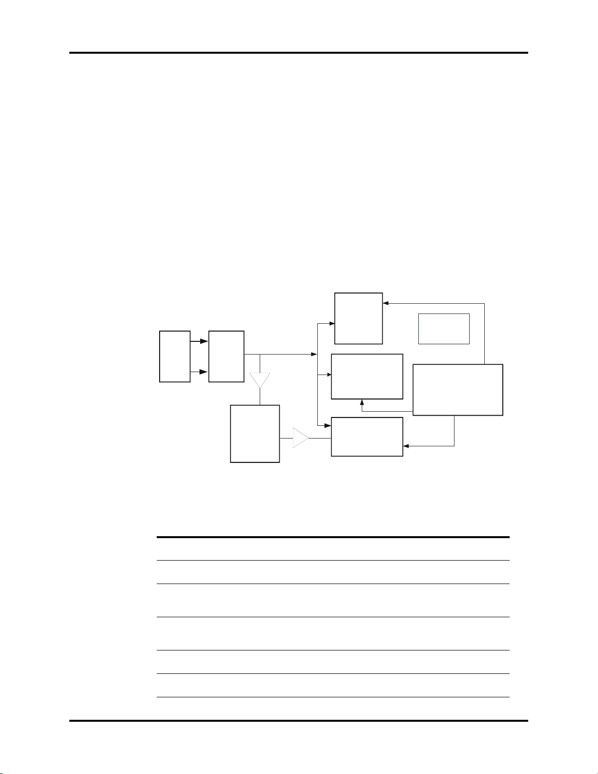
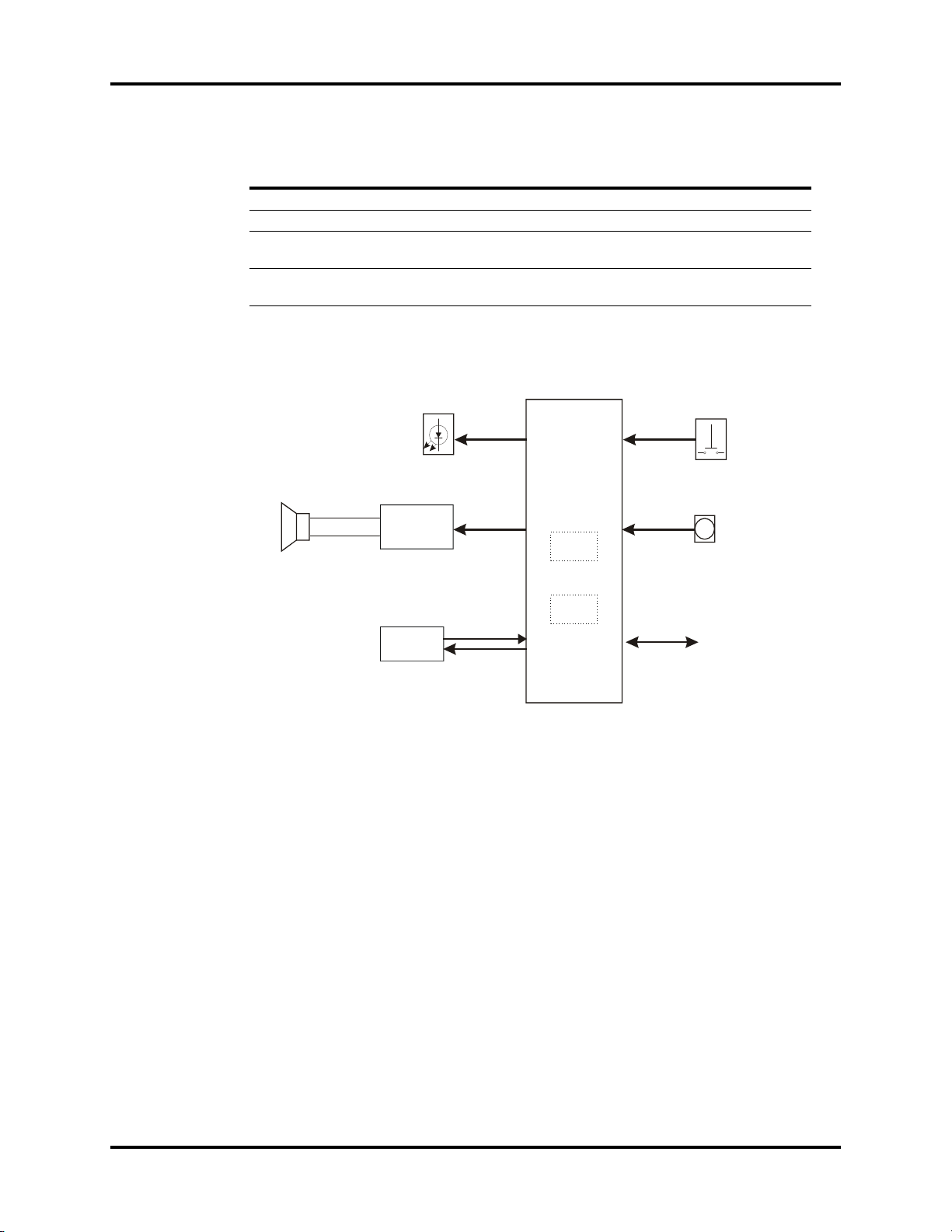
1.0
Display
Recorder
Keyboard
Main
control
board
Power
Network
interface
(future)
ECG/RESP/TEMP NIBP
SpO
2
IBP
Medical Staff
Patient
Theory of Operation
1.1 Introduction
The Trio portable patient monitor uses a parameter module as the basis for acquiring patient
data. The results are transmitted to the main control board to process and display the data
and waveforms. CPU board commands and status messages of modules are transmitted via
databus. The structure of the entire system is shown in the figure below.
Trio™ Service Manual 0070-10-0591-01 1 - 1
FIGURE 1-1 System Structure Diagram

Introduction Theory of Operation
As shown in the above figure, the four parameter modules execute real-time monitoring of
NIBP, SpO
, ECG/RESP/TEMP and IBP through the use of blood pressure cuffs and patient
2
cables. The patient data is transmitted to the CPU board for display. When required, data
may be printed out via the recorder.
1 - 2 0070-10-0591-01 Trio™ Service Manual
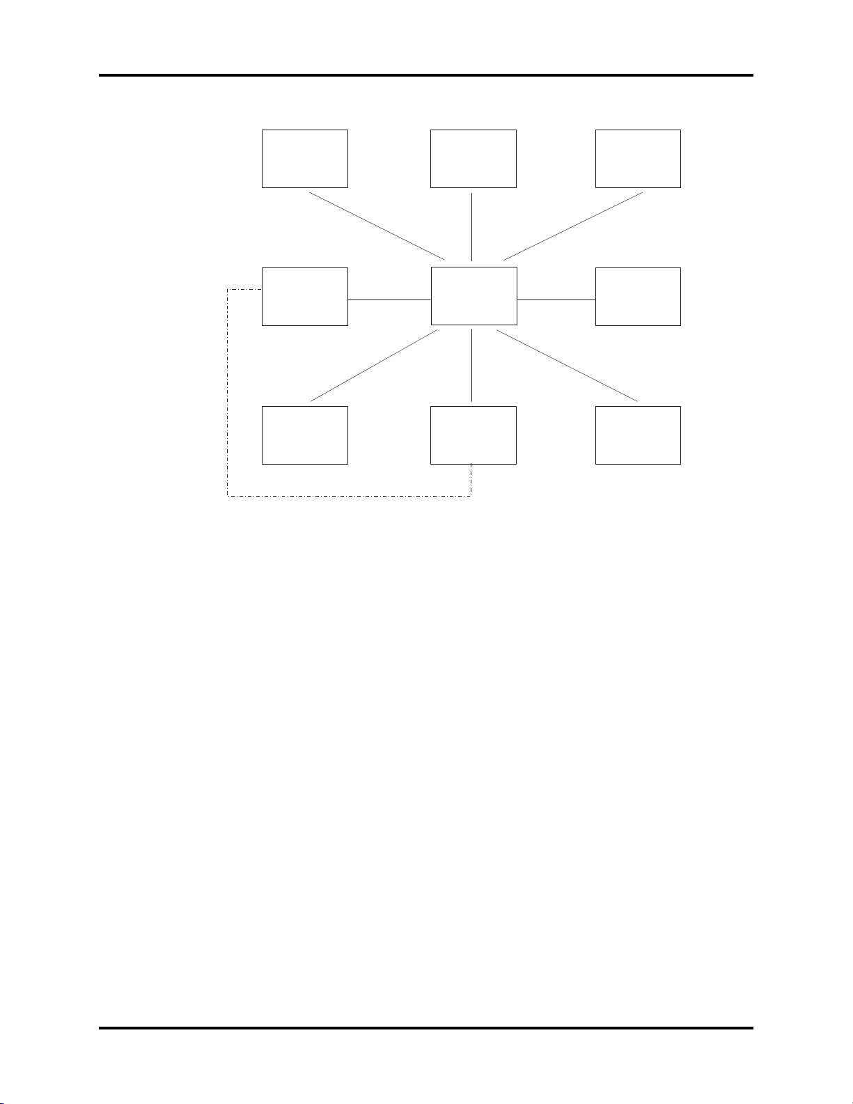
Theory of Operation Hardware Overview
Host P .C.B .
ECG/RES
P/TEMP
P. C. B .
SPO2
NIBP
Module
IBP
P.C . B.
TFT Display
83 inchs
800 X 600
4
Power Supply PCB
Key &
Alarm P
.C.B .
Recorder Modul e
Recorder P.S.
Battery
ECG
IBP
NIBP
SPO2
VGA
interface
Analog
output
Speak er
Alarm
LED
P5P
10
P13
P8
P14
P9
P6
P
17 (FOR 509C)
P11
P12
NET
Interface
P15
J2
J3
P16
J6
J5
J4
J7
J9
J8
X
1
X
2
X
3
X4
X5 X6
X7
X8
X9
X10
X11 X21
X14
X15
X16
P1
P2 (CRT)
A4(TFT_DIGTAL)
P3 (FOR 9000
VGA)
P7(BDM
)
ECG
Cable
SpO2
Sensor
Cuff
IBP Cable
Main
Power
Input
TO
X4
From J2
FAN
TEMP
TEMP
Sensor
Serial Coverter
P.C . B
J2
J
1
Serial
interface
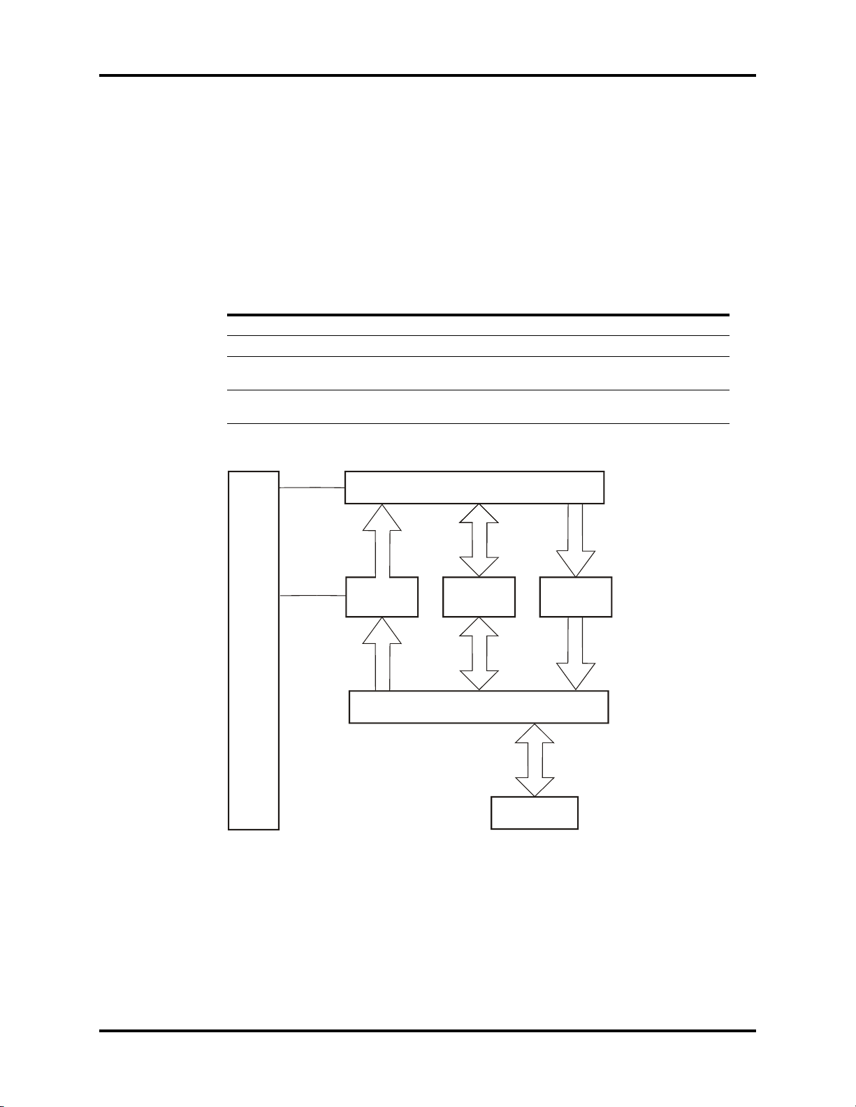
1.2 Hardware Overview
FIGURE 1-2 Connection Diagram
1.2.1 Power Supply Board (Lead Acid Battery)
P/N 0671-00-0235
Trio power supply board specifications:
•AC input voltage:100~250 VAC
•AC input current: <1.6 A
•AC voltage frequency: 50/60 HZ
•Two-way output voltage: 5 V/12 V, normal working current is 1.5 A for 5 V, 2 A
for 12 V
•Two-way output voltage has functions of short-circuit, over-current and over-voltage
protection
•The power board has reset function
•The power board can manage the charging process of lead-acid battery
(12 V/ 2.3 AH). The charging time is 8 hours maximum.
NOTE: Power Supply Board must be connected to resistive load to
operate properly and avoid damage due to an overcurrent
condition.
Trio™ Service Manual 0070-10-0591-01 1 - 3
Hardware Overview Theory of Operation
AC
input
AC/DC
12V output
REC POWER
SOURCE
Power on/off
control circuit
5VDC-DC
converter
Voltage
test
Battery
and
Charging
Management
Circuit
FIGURE 1-3 Block diagram of Trio power supply board
Key Test Points
NO. NAME LOCATION FUNCTION
1Rectified voltageC12 Primary rectified voltage, range: 107~354 V
2RTN1 C12 negative
3Driving
waveform
4VIN C19 positive
5GND C19 negative
65B C47 positive
75 V ZD3 cathode 5 V output, voltage range is 4.75~5.25 V
812 V ZD3 cathode 12 V output, voltage range is 11.0~13.0 V
electrode
Q1.1 There is a driving waveform of about 100 KHZ
electrode
electrode
electrode
Primary ground
between Q1.1 and the negative electrode of C12
17.5 V provide input voltage for DC-DC
Secondary ground
5 V spare output, provide power for on/off circuit
1 - 4 0070-10-0591-01 Trio™ Service Manual
Theory of Operation Hardware Overview
AC
input
AC/DC
Li-ion
Battery and
Charging
Managerent
circuit
12V output
REC POWER
SOURCE
Power on/off control
circuit
5VDC-DC
BUCK
converter
Volta ge tes t
1.2.2 Power Supply Board (Lithium Ion Battery)
P/N 0671 -00-0051
Trio Power Supply board specifications:
•AC input voltage:110~240VAC+10%
•AC input current: <1.6A
•AC voltage frequency: 50/60+3HZ
•Two-way output voltage: 5V/12V, normal working current is 1.3A for 5V, 1.3A for
12V.
•Two-way output voltage has functions of short-circuit, over-current and over-voltage
protection.
•The power board has reset function.
•The power board can manage the charging process of li-ion battery (11.1V/4.4AH).
The charging time is 6.5 hours maximum.
FIGURE 1-4 Block diagram of Trio power supply board
Key Test Points
NO. NAME LOCATION FUNCTION
1Oscillator
2GND CC61 negative
3D-S waveformQ1.2 There is a waveform of about
4Driving
5Rectified
6VIN C18 positive
frequency
waveform
waveform
Pin 4 of U1 Generate a oscillating frequency about 100kHZ
electrode
Q1.1 There is a driving waveform of about 100KHZ,
D5 anode Secondary rectified voltage
electrode
Primary Ground
100KHZ,107~354V between Q1.2 and the
negative electrode of C12
15V between Q1.1 and the negative electrode of
C12
17.6V,provide input voltage for DC-DC
Trio™ Service Manual 0070-10-0591-01 1 - 5

Hardware Overview Theory of Operation
Key Test Points
NO. NAME LOCATION FUNCTION
712V C41 positive
85V C58 positive
9Feedback
voltage
electrode
electrode
R37 positive
electrode
12V output, voltage range is 11.0~13.0V
5V output, voltage range is 4.75~5.25V
There is a DC waveform of about 2.5V between
R37
1.2.3 CPU Board (Main Control Board)
P/N 0671-00-0056 or P/N 0671-00-0236
1.2.3.1 Overview
Power Supply Input Voltage: +12 V±5%; +5 V±5%
The main control board uses the Coldfire series embedded microprocessor 5206e
manufactured by Motorola Company. It also adopts 3.3 V low-voltage power supply to
reduce the power consumption. Other main components on the main control board include:
Flash, SRAM, FPGA, network controller, etc., all of which require 3.3 V power. The capacity
of the Flash is 2 MB or 4 MB*, which employs two parallel-connected 512K x 16 or 1M x
16* chips and therefore uses 32-bit character width to support CPU to operate at the highest
possible speed instead of accessing the DRAM for operation. The main control board has
also a 4 MB memory, which is made up of two parallel-connected 1M ×16-bit chips.
Because no executing program is required to be loaded, only one RTC is used. This chip uses
one 225maH dry cell as the spare power supply. In addition, one 2KB E2PROM is used to
store parameters. The main control board supports a resolution of 800 x 600 and provides
three interfaces: a LVDS interface, a 6 bit digital interface, and a VGA interface. The monitor
displays characters and waveforms, in the same color, on the screen. The support system
needs 10 serial ports, and the baud rate (4800/9600/19.2 K/38.4 K/76.8 K) can be
selected by software and interface buffer drives. The main control board adopts the network
controller AX88796 (3.3 V, 10 MHz), which has inside 16 K high-speed buffer SRAM. The
MAX5102 8-bit single-way D/A converter is used to fulfill analog output. The 5 V and 12 V
regulated voltage supplies are introduced from the power board, and therefore 3.3 V and
2.5 V working supplies are respectively generated. Among them, 2.5 V is to be used for the
internal verification of FPGA.
*Applies to P/N 0671-00-0056.
1 - 6 0070-10-0591-01 Trio™ Service Manual
Theory of Operation Hardware Overview
Flash/SRAM
Network
controller
Audio
alarm/spare
battery
DRAM
RTC/E PROM
2
Interrupt
management
circuit
I/O serial
interface
CPU
FPGA
Display
driving
circuit
FIGURE 1-5 Block Diagram of Trio CPU board
1.2.3.2 Detailed Description
3.3 V low-voltage power supply component is used. The external power is 5 V, which is
converted by the DC/DC converter into 3.3 V and 2.5 V, the latter voltage being especially
used for FPGA. The main control board is connected to external devices via corresponding
interfaces and input: the power supply connected to the interface board, the 9-way serial
port, TFT interface, analog VGA interface, network interface, analog output and a spare
serial port, etc. The BDM interface, on the board, is reserved for the purpose of software
testing and downloads.
CPU
Uses Coldfire 5206e. Clock rate is 54 MHz, working voltage is 3.3 V.
FLASH
Uses two parallel-connected 512K x 16 or 1M x 16* FLASH memories. The output terminal
PP1 of CPU is used to realize write-protection of FLASH. It is effective in low-level state.
*Applies to P/N 0671-00-0056.
DRAM
The Trio CPU main control board uses two parallel-connected 1M x 16 DRAM, which
construct 4M address space.
Trio™ Service Manual 0070-10-0591-01 1 - 7

Hardware Overview Theory of Operation
Display
The resolution is 800 x 600. Frequency is 38 MHz. It works in an appropriate SVGA mode.
VRAM adopts 16-bit structure and is divided into an alphanumeric character screen and a
waveform screen. To the left of the alphanumeric character screen is the corresponding
waveform screen. The character screen is used to display data and flashing alarming
parameters. The user can select the color of the waveform and alphanumeric characters for
each parameter.
LVDS Interface
By utilizing time-share sampling, the LVDS (Low Voltage Differential Signaling) interface
converts multi-channel CMOS/TTL signals into single channel, low-voltage, double-frequency
differential signals. LVDS interface is generally realized by a special integrated circuit. The
special LVDS chip used for display is DS90CF363A. This chip converts 18-bits of RGB data
and 3 bits of LCD timing and control data (21 bits of CMOS/TTL data) into 3 LVDS data
streams. Four differential signals including the 3 data streams and a phase-locked frequency
are transmitted to the display screen. The working frequency of DS90CF363A is 20~65
MHz.
Reset and Parameter Storage
The CPU board uses an integrated chip CAT1161, which controls both power-on reset and
parameter storage. This chip has an E2PROM with the capacity of 2K. It can be used to
modify and store various nonvolatile parameters of the host. The power-on reset and
WAT CH DO G f un ct io ns a re us ed to re al iz e r es et fu nction of the CPU board. When J1 is open
circuit, the software can also disable WATCHDOG by using the output signal PP0 of CPU in
order to realize the self test of WATCHDOG. The bus interface of this chip is I2C.
Network Controller
The network controller adopts special chip AX88796. Its working clock is 25 MHz. It also
has internal 16 K high-speed buffer SRAM. The data bus of this chip is 16-bit width.
Key Test Points
NO. NAME FUNCTION
1V33Digital supply voltage: +3.3 V
2V25FPGA supply voltage: +2.5 V
3V3 Lithium battery voltage: +3 V
4CLK CPU master clock: 54 MHz
5PCKFPGA and display clock: 38 MHz
6NCKNetwork chip clock: 25 MHz
7/RSTSystem reset signal
8/NINTNetwork chip interrupt signal
9DO Signal indicating successful FPGA configuration
1 - 8 0070-10-0591-01 Trio™ Service Manual
Theory of Operation Hardware Overview
CPU
(AT89C2051)
RAM
128 x 8
FLASH
4KX8
Watch dog
button and encoder
scan circuit
serial communication
Main control board
button
signal input
Sound
Effect
Control
speaker
Alarm indicator
control circuit
ENCODER
BUTTON
Volu me
Control
Lowpass
and
Bandpass
Filter
Power
Amplifier
LM386
1.2.4 Keypad Board
P/N 0671-00-0237
FIGURE 1-6 Keypad Block Diagram
1.2.4.1 Detailed Description
This circuit has three main parts:
1. Alarm Audio Signal Circuit: The alarm audio signal circuit is made up of components
including U3, U6, R8, R25, E6 (E1), R11, R12, R3 and R32. P3.3 is used to control the
length of the alarm sound. R8, E1 and E6 are used to generate the rise edge and the fall
edge of the sound signal. Q1 is used to make the rise edge and fall edge of the lowlevel alarm slower than those of medium/high-level alarm. D1 is used to generate the
heart beat and pulse tone. If P3.2 is high, the alarm square waveform of P3.5 will pass
and, as a result, control P3.2 to generate a "heart beat tone" or ‘‘rotary encoder tone’’.
R11, R12, R3, R32 and R18 together construct a variable voltage-dividing network
which, by controlling the state of RA and RB via U3, determines the sound volume level.
2. RC Bandpass Filter/Audio Amplifier: A one-stage RC bandpass filter is used to block the
low frequency component of the alarm signal (700 Hz. square wave) before it is input to
the audio amplifier, LM386. This bandpass filter is made up of R13, R28, C9, C15, RA
and the input resistance R in of LM386.
3. Alarm Indicator Control/Encoder and Key Scanning: The flashing of the alarm indicator
in red or green is controlled by the state of microchip P1.6 and P1.7. The
microprocessor scans the state of microchips P1.0~P1.2 to determine which key, or if
the encoder, is pressed. The microprocessor scans the state of microchips P1.4 and P1.5
to determine if the encoder is turned and in which direction it is turned.
Key Test Points
NO. NAME LOCATION FUNCTION
1VCC P4.4 Power input, range: 4.8~5.1V
2GND P4.5 Power supply and signal ground
3RST U1.1 CPU reset signal. At low level (<0.3V) when
4Crystal oscillatorX1.1, X.2 CPU crystal oscillator. Sine wave (1.5~3.5V)
operating normally
when operating normally
Trio™ Service Manual 0070-10-0591-01 1 - 9
Hardware Overview Theory of Operation
Watch dog
ENCODER
KEY
CPU
(AT89C51)
RAM
128 X 8
FLASH
4K X 8
Main Control
board (Host CPU Board)
Audio Process
Circuit
SPEAKER
LED
1.2.5 Keypad Board
P/N 0671-00-0058
FIGURE 1-7 Keypad block diagram
1.2.5.1 Detailed Description
This module detects key and encoder input signals, converts them into code then sends these
coded signals to the main board. The main control board (Host CPU board) in turn sends
commands back to the keyboard's control indicator and audio process circuits, which enable
or disable audio and visual alarm respectively, as required.
CPU
•Detects key and encoder input signals;
•Controls LED status;
•Controls Audio Process Circuit;
•Regularly zeroes Watchdog Timer;
•Communicates with main board.
Audio Process Circuit
Generates audio signals to drive the speaker.
Watchdog
•Upon power-up, supplies Reset signal to CPU;
•Provide functions of Watchdog Timer Output and voltage detection.
1 - 10 0070-10-0591-01 Trio™ Service Manual
Theory of Operation Hardware Overview
Watch dog
ENCODER
KEY
CPU
(PIC16F73)
RAM
192 X 8
FLASH
4K X 4
Main Control
board (Host CPU Board)
Audio Process
Circuit
SPEAKER
LED
Key Test Points
NO. NAME LOCATION FUNCTION
1VCC P4.4 Power input, range: 4.8~5.2V
2GND P4.5 Power supply and signal ground
3RST U1.10 CPU reset signal. At low level(<0.3V) when
4Crystal oscillatorX1.1,X.2 CPU crystal oscillator. Sine wave signal
operating normally
(1.5~3.5V) when operating normally
1.2.6 Keypad Board
P/N 0671-00-0064
FIGURE 1-8 Keypad block diagram
1.2.6.1 Detailed Description
This module detects keypad and encoder input signals, converts them into code and transmits
the code to the Host CPU board. The Host CPU board sends commands to the keyboard
which in turn controls the indicator and audio process circuits, activating audio and visual
alarms accordingly.
CPU
Trio™ Service Manual 0070-10-0591-01 1 - 11
The Keypad Board's CPU is responsible for the following functions:
•Detects keypad and encoder input signals
•Controls LED status
•Controls Audio Process Circuit
•Regularly zeroes Watchdog Timer
•Communicates with main board.
Hardware Overview Theory of Operation
Thermal Head
CPU
cpld 9536
Status Detec tion
Motor
driver
Signal & 5 V
DC/DC
12 V > 8 V
Audio Process Circuit
Generates audio signals to drive the speaker.
Watchdog
•Upon power-up, supply Reset signal to CPU
•Provide functions of Watchdog Timer Output and voltage detection.
Key test points
NO. NAME LOCATION FUNCTION
1.
2.
3.
4.
5V/5B J5 pin 1 Power input, range: 4.0~5.5V
GND J5 pin 2 Power supply and signal ground
RST J5 pin 3 CPU reset signal. At low level(<0.8V (during
normal operation)
Crystal oscillator X1 pin 1,X1 pin 2 CPU crystal oscillator. Sine wave signal
1.5~3.5V (during normal operation)
1.2.7 TR60-C Recorder
FIGURE 1-9 Block Diagram of TR60-C drive board
1.2.7.1 Detailed Description
Thermal Head
The thermal head, the core component in the TR60-C recorder, is the PTMBL1300A thermal
head, manufactured by the ALPS company.
1 - 12 0070-10-0591-01 Trio™ Service Manual

Theory of Operation Hardware Overview
CPU System
The CPU system is the core of the drive board. Its task is to receive the data from the host and
generate lattice messages after calculation using a specified algorithm. These messages are
then sent to the thermal head for printing. The CPU system can simultaneously collect data
from both the thermal head and the drive board and display data sent to the host.
Power Conversion
The recorder requires the system to provide two voltages: 12 V and 5 V. The 5 V is directly
driven by the logic and analog circuit of the drive board and the thermal head. Its current is
less than 150 mA. The 12 V is converted into 8 V (by the DC/DC on the board) to drive the
thermal head and the motor. The current required is determined by the printing content and
ranges from 0.5 A to 2 A.
Motor Drive
A small motor is used to control the paper movement at the thermal head. The processor on
the drive board uses two motor drives IC LB1843 V to control and drive the motor. These two
IC’s use constant current to control and drive the motor.
Status Detection
To c or re ct ly a nd s af el y co nt ro l an d dr iv e th e th er ma l he ad and t he m ot or, t he d ri ve b oa rd
must use the sensor inside the thermal head to detect the following signals: the position of the
chart paper, if the chart paper is installed and if the temperature of the thermal head has
exceeded the limit.
Key Test Points
NO. NAME LOCATION FUNCTION
112 V JP3.1 Power input, range: 10~18 V
2GND JP3.2 Power and signal ground
3 VPP U7.8 Power supply for heating thermal head and
4VCC U1.14 +5 V supply: 4.75~5.25 V
5RESETU3.10 CPU reset signal. At high level(>2.4 V) after
drive motor: 7.8 V~8.4 V
power-on
Trio™ Service Manual 0070-10-0591-01 1 - 13
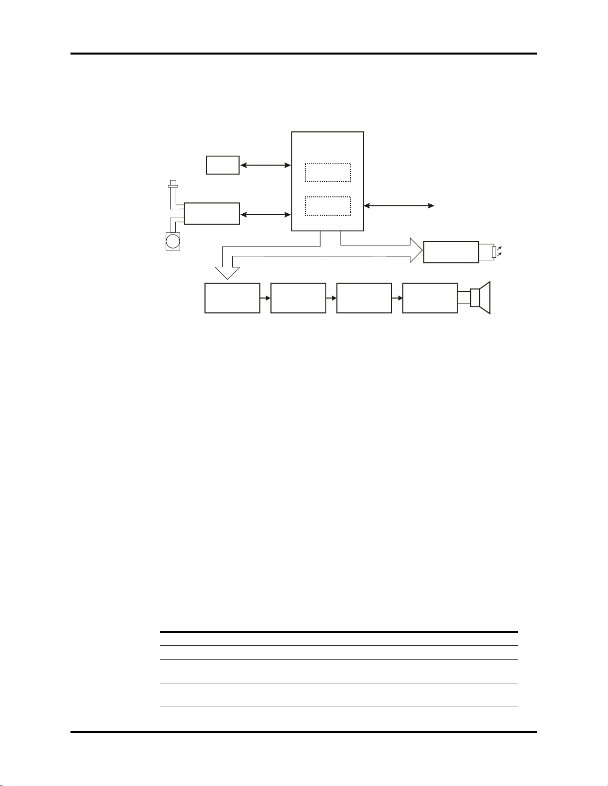
Serial Interface Converter Board Theory of Operation
Host P .C.B.
P5
P10
P13
P8
P1 4
P9
P6
P1 7 ( F O R 5 0 9 C )
P11
P1 2
P1 5
P1 6
P1
P2 ( C R T )
P4(T FT_DIGTA L )
P3(FOR 900 0
VGA)
P7(BDM
)
Serial Coverter
P.C.B
J2
J1
Serial
interface
Converter Board
Tx
Rx
G
5V
Tx
Rx
G
TTL Level
RS232 Level
DB9 Socket
RS232
Converter
chip
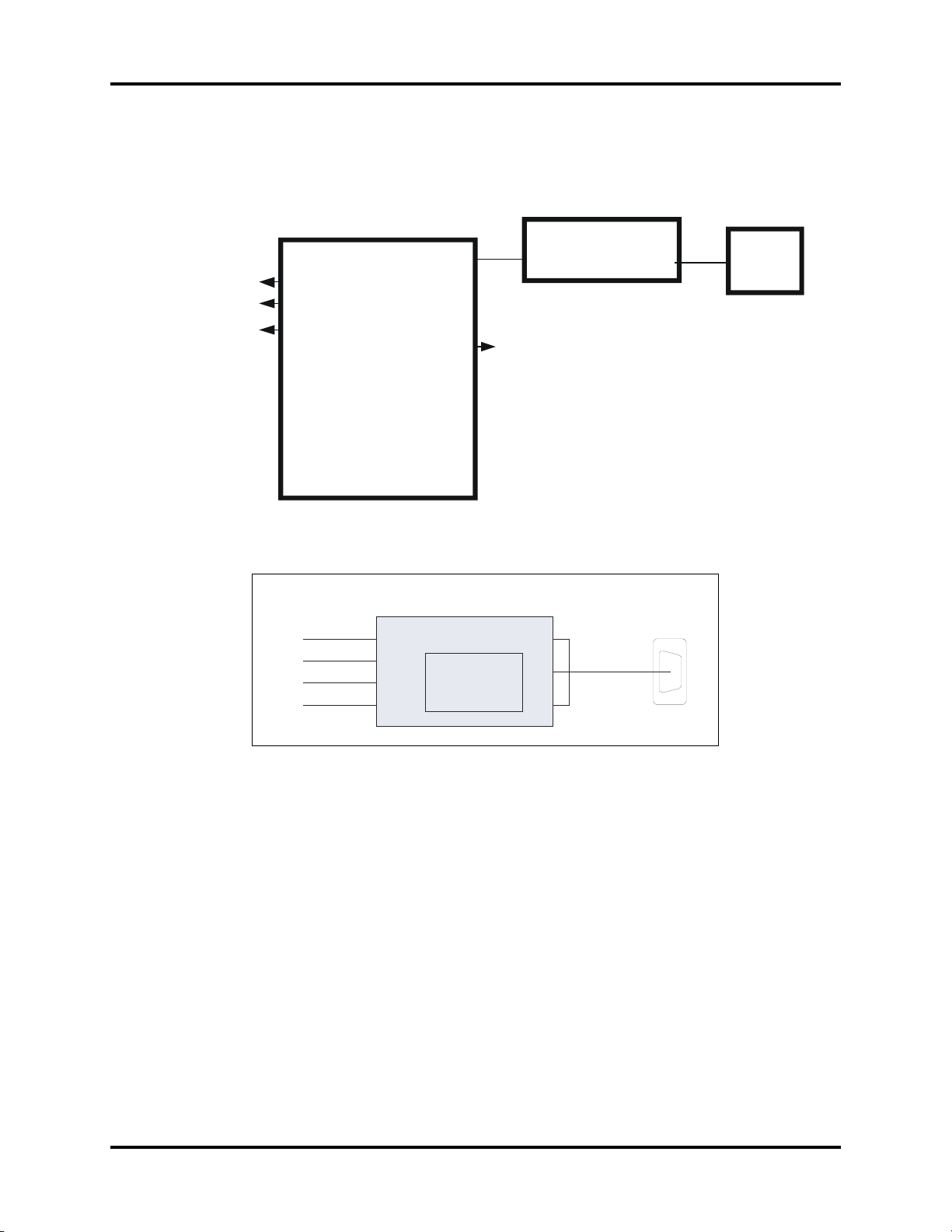
1.3 Serial Interface Converter Board
The Serial Interface Converter Board is used to convert the TTL level (5V) to RS232 level.
1 - 14 0070-10-0591-01 Trio™ Service Manual
FIGURE 1-10 Serial Interface connection diagram
FIGURE 1-11 Block diagram of Serial Interface Converter Board

Theory of Operation Parameter Circuit Descriptions
1.4 Parameter Circuit Descriptions
1.4.1 ECG
The main functions concerning ECG are:
•Lead: 3-lead, 5-lead
•Lead Method; I, II, III, avR, avL, avF, V, CAL
•Floating Input
•Right-Leg Drive
•Lead-off Detection
The ECG circuit is responsible for processing the ECG signals of human body. The circuit
consists of following parts:
Input Circuit: The ECG electrodes are connected into the circuit through the cable.
This circuit is mainly used to protect ECG input stage and filter the signals so as to
remove the outside interference.
Buffer Amplifying Circuit: Used to convert the impedance of ECG signals, so as to
ensure that the ECG has a very high input impedance but only low output impedance.
Right-Leg Drive Circuit: The middle output point of the buffer amplifying circuit is
reversely amplified and then fed to the RL of the 5-lead ECG to maintain the human body
in a equipotential state. This method can reduce the interference and raise the commonmode rejection ratio of the circuit.
Lead-off Detection: Based on the theory that the lead-off may cause the output of the
buffer amplifying circuit to change, we can use the comparator to accurately determine
if the lead has fallen off. In this way, the level can also be converted into TTL level for the
MPU to test.
Main Amplifying Circuit: A measurement amplifier consisting of three standard
operation amplifiers.
Last Stage Processing Circuit: Used mainly to couple ECG signals, program control
of the gain amplifier, filter the waveform and move the level, amplify the signal and send
it to the analog-to-digital converter.
1.4.2 Respiration
Respiration is measured by the thoracic impedance method. When a person is breathing, his
chest moves up and down. This movement equals the impedance change between electrodes
RA and LL. The monitor converts the high-frequency signals passing through RA and LL into
amplitude-modulated high-frequency signals, which are then demodulated and amplified into
electronic signals varying with the respiration changes and then transmitted to analog-digital
converter. The RESP module is made up of a respiration circuit board and a coupling
transformer. The circuit includes stages such as: oscillation, coupling, demodulation,
preliminary amplification and high-gain amplification.
Trio™ Service Manual 0070-10-0591-01 1 - 15

Parameter Circuit Descriptions Theory of Operation
1.4.3 NIBP
The monitor measures non-invasive blood pressure using the oscillometric method. Detailed
measurement procedures follows:
1. Inflate the cuff encircled around the upper arm until the pressure in the cuff blocks the
blood flow in the artery of the upper arm.
2. Then deflate the cuff according to the requirement of the algorithm.
3. With the pressure decreasing in the cuff, the arterial blood will palpitate with the pulse,
which results in pulsation in the cuff. Through the pressure sensor, connected to the
bladder of the cuff, a pulsation signal synchronous with the patient's pulse will be
generated.
4. After being filtered by a high-pass filter (about 1 Hz), this signal becomes the pulsating
signal and is amplified. The amplified signal is then converted into a digital signal by
the A/D converter.
5. After processing this digital signal, systolic pressure, diastolic pressure and mean
pressure can be obtained. To avoid measurement errors, choose appropriate cuffs for
patient size. The NIBP module also has an overpressure protection circuit to prevent the
cuff from being inflated to a very high pressure.
The main operating modes of NIBP are:
A. Adult/Pediatric
B. Manual Measurement
C. Interval Measurement
1.4.4 SpO
SpO2 Plethysmograph measurement is employed to determine the oxygen saturation of
hemoglobin in the arterial blood. If, for example, 97% hemoglobin molecules in the red
blood cells of the arterial blood combine with oxygen, then the blood has a SpO
saturation of 97%. The SpO
shows the percentage of hemoglobin molecules which have combined with oxygen
molecules to form oxyhemoglobin. The SpO
signal and a plethysmograph. Arterial oxygen saturation is measured by a method called
pulse oximetry. It is a continuous, non-invasive, method based on the different absorption
spectra of reduced hemoglobin and oxyhemoglobin. It measures the amount of light that is
transmitted through patient tissue (such as a finger or an ear).
Select according to the patient size, weight and age.
Manual measurement is also called single measurement. It means the monitor only
performs one measurement for each time the NIBP key is pressed.
Interval measurement means to perform one measurement within selected time cycle.
Time intervals can be set up as: 1, 2, 3, 4, 5, 10, 15 and 30 minutes, 1, 2, and 4
hours, OFF, CONT. (Continuous). If set to continuous, the monitor will perform a
measurement continuously for 5 minutes then revert to an interval setting of 5 min.
Continuous measurement is effective in monitoring changes in blood pressure.
2
oxygen
2
numeric on the monitor will read 97%. The SpO2 numeric
2
/Pleth parameter can also provide a pulse rate
2
1 - 16 0070-10-0591-01 Trio™ Service Manual

Theory of Operation Parameter Circuit Descriptions
The sensor measurement wavelengths are nominally 660 nm for the Red LED and 940 nm for
the Infrared LED. Maximum optical power output for LED is 4 mW. The amount of light
transmitted depends on many factors, most of which are constant. However, one of these
factors, arterial blood flow, varies with time because it is pulsating. By measuring the light
absorption during a pulsation, it is possible to derive the oxygen saturation of the arterial
blood. Detecting the pulsation gives a pleth waveform and pulse rate signal. The SpO
and the pleth waveform can be displayed on the main screen.
value
2
1.4.5 Temperature
The temperature circuit can amplify and filter the input signal of the temperature probe and
then output it into the A/D sampling circuit on the ECG/RESP board. This circuit consists of
sampling switching, constant-current supply, signal amplifier, filter and probe detector. The
output signal of the circuit has clamping protection to ensure that the output voltage is less
than VCC. The circuit also has a self-calibrating function.
1.4.6 IBP (optional)
Invasive Blood Pressure monitors arterial pressure, central venous pressure and pulmonary
arterial pressure.
IBP may be measured by inserting the catheter into the appropriate blood vessel. The end of
the catheter, located outside the human body, should connect directly to the pressure
transducer.
Inject normal saline into the catheter. Since the liquid can transfer pressure, the pressure
inside the blood vessel can be transferred to the outside pressure transducer. In this way we
can obtain the waveform of the dynamic pressure inside the vessel. Systolic, diastolic and
mean pressures are calculated by using an algorithm.
Trio™ Service Manual 0070-10-0591-01 1 - 17

Parameter Circuit Descriptions Theory of Operation
This page intentionally left blank.
1 - 18 0070-10-0591-01 Trio™ Service Manual

2.0
Calibration/Maintenance
2.1 Calibration Introduction
The following procedures are provided to verify the proper operation of the Trio Monitor. A
menu driven interface is used to execute all verification tests.
2.2 Warnings and Guidelines
In the event that the instrument cover is removed, observe these following warnings and
general guidelines:
1. Do not short component leads together.
2. Perform all steps in the exact order given.
3. Use extreme care when reaching inside the opened instrument. Do not contact exposed
metal parts which may become ‘‘live’’.
4. Read through each step in the procedure, so it is understood prior to performing the
step.
2.3 Test Equipment and Special Tools Required
•Digital or Mercury Manometer w/bulb and valve 0-300 mmHg
•Test Chamber/Dummy Cuff (P/N 0138-00-0001-03)
•DVM
•Patient Simulator
•Safety Analyzer (Dempsy Model 431 or Equivalent)
•Metric Ruler
•PC or Laptop w/Windows 98 or above, CD-ROM drive, and Ethernet card installed
Trio™ Service Manual 0070-10-0591-01 2 - 1

Calibration and System Checks Calibration/Maintenance
2.4 Calibration and System Checks
2.4.1 Device Appearance and Installation Checks
Inspect the Trio Monitor to ensure that:
•The outer housing of the device is clean and has no scratches or cracks
•When shaking the device, there are no loose components
•All keys are smooth and free for operation
•Labels are complete, sufficient and accurate
•Standard configuration is complete and all connectors are installed securely
2.4.2 Maintenance Menu
The MAINTENANCE menu provides access to all user operable calibration checks. It also
provides access to certain technical information and settings. To access the
MAINTENANCE menu, turn the unit on, rotate the Navigator™ knob to highlight the
MENU icon at the bottom of the screen and push the knob to select the SYSTEM MENU.
From the SYSTEM MENU, select MAINTENANCE.
FIGURE 2-1 Maintenance Menu DIAP units (S/N MC15000-XX and above)
2 - 2 0070-10-0591-01 Trio™ Service Manual

Calibration/Maintenance Calibration and System Checks
FIGURE 2-2 Maintenance Menu (below S/N MC15000-XX)
2.4.2.1 Calibrations
Calibrations should be performed at least once a year. Calibrations should also be
performed after any preventive maintenance or repair of the Trio Monitor.
From the MAINTENANCE menu make the following selections to perform each specific
calibration or check.
Trio™ Service Manual 0070-10-0591-01 2 - 3

Calibration and System Checks Calibration/Maintenance
IBP Pressure Cal
The purpose of this calibration is to ensure that the system gives you accurate measurements.
FIGURE 2-3 IBP Calibration
WAR N I NG: Ne v e r perfor m this procedur e while p a tient i s being
1. Connect a Pressure Transducer Interface Cable from a Pressure Transducer
(Figure 2-3) to the IBP socket on the right side panel of the Trio
2. Open 3-Way Stopcock to atmosphere.
3. Perform zeroing procedure by selecting the IBP parameter menu, then selecting IBP
ZERO tile.
4. From IBP ZERO menu select IBP ZERO tile to zero the blood pressure channel.
5. Connect a Sphygmomanometer or a digital Manometer w/bulb to the Pressure
Transducer via a T fitting.
6. Close the 3-way Stopcock.
7. Manually pump the Manometer to a static value of 100 mmHg and close valve on bulb.
8. From the MAINTENANCE menu, select IBP PRESSURE CAL.
9. From IBP PRESSURE CAL menu, select the tile adjacent to CAL VALUE and set to 100
mmHg.
monitored.
2 - 4 0070-10-0591-01 Trio™ Service Manual

Calibration/Maintenance Calibration and System Checks
FIGURE 2-4 IBP Pressure Calibration Menu
10. Select CALIBRATE. The monitor will perform the calibration and display one of the
following calibration completion messages.
MESSAGE DESCRIPTION
SUCCESSFUL CALIBRATE Indicates Blood Pressure was calibrated successfully. No
SENSOR OFF, FAIL Check that sensor is connected, then proceed with
IN DEMO, FAIL Check that the monitor is not in DEMO mode. If message
PRESSURE OVER RANGE, FAIL Check that you have selected appropriate transducer value
further action required.
calibration. If message does not clear contact Customer
Service.
does not clear contact Customer Service.
in IBP CAL, then proceed with calibration. If message does
not clear contact Customer Service.
Trio™ Service Manual 0070-10-0591-01 2 - 5

Calibration and System Checks Calibration/Maintenance
DIGITAL OR
MERCURY
MANOMETER
500 ml.
TEST CHAMBER
P/N 0138-00-0001-03
BULB
hose
TRIO MONITOR
NIBP
NIBP CAL
Connect a test chamber (P/N 0138-00-0001-03) and a calibrated digital mercury
manometer with bulb via T fitting to the NIBP quick connect fitting of the Trio Monitor
(Figure 2-5.)
1. From the MAINTENANCE menu select NIBP CAL. The selected tile will now read
STOP CAL. The user may select this tile at any time to stop the test.
2. Using the bulb, inflate the pneumatic system so that the digital mercury manometer reads
0, 50 and 200 mmHg in turn. The difference between the indicated pressure of the
digital mercury manometer and the indicated pressure in the NIBP parameter tile of the
Trio Monitor should not exceed 3 mmHg. If it exceeds 3 mmHg, please contact a
service technician.
FIGURE 2-5 Diagram of NIBP Calibration
2 - 6 0070-10-0591-01 Trio™ Service Manual

Calibration/Maintenance Calibration and System Checks
P/N 0138-00-0001-03
hose
TRIO MONITOR
NIBP
TEST
CHAMBER
NIBP Pneumatic
WARNING: The NIBP pneumatic test (specified in the EN 1060-1
standard) is used to determine if there are air leaks in the
NIBP airway. If the system displays the prompt that the
NIBP airway has air leaks, please contact the manufacturer
for repair.
1. Connect a test chamber (P/N 0138-00-0001-03) to the NIBP quick connect fitting on the
Trio Monitor (Figure 2-7).
2. From the MAINTENANCE menu, select NIBP PNEUMATIC. The NIBP pump will
begin to run and the message STOP PNEUM will appear in the selected tile. The user
may select this tile at any time to end the test.
FIGURE 2-6 Maintenance Menu
3. The prompt Pneum testing… will appear at the bottom of the NIBP parameter area
indicating that the system has started performing the pneumatic test.
4. The system will automatically inflate the pneumatic system to about 180 mmHg.
After approx. 20 seconds, the system will automatically deflate, marking the completion of
the test.
If no message appears at the bottom of the NIBP parameter area, no air leaks exist.
If the message PNEUMATIC LEAK appears at the bottom of the NIBP parameter area, the
NIBP module may have air leaks. The user should first check for loose connections.
After confirming connections, the user should repeat the pneumatic test. If the PNEUMATIC
LEAK message still appears, please contact the manufacturer for repair.
FIGURE 2-7 Diagram of NIBP Air Leakage Test
Trio™ Service Manual 0070-10-0591-01 2 - 7

Calibration and System Checks Calibration/Maintenance
ECG Cal
1. Set ECG lead to I and ECG size to x1.
2. From The MAINTENANCE menu select ECG CAL. The message CALIBRATION
MODE will appear in red at the lower left of the ECG waveform area. The highlighted
tile will now read STOP CAL. The user may select this tile at any time to end the test.
3. A 1mV peak to peak square wave will appear in the ECG waveform area. This is the
Cal Pulse.
4. Measure the amplitude of the Cal Pulse with a metric ruler. The Cal Pulse should measure
1 cm +/- 5%.
5. Set ECG size to x 2. Cal Pulse should measure 2 cm +/- 5%.
6. Set ECG size to x .25. Cal Pulse should measure 25 mm +/- 5%.
7. Set ECG size to x .5. Cal Pulse should measure 50 mm +/- 5%.
8. If any measurements are out of tolerance range, please contact the manufacturer for
repair.
2.4.2.2 Technical Information and Settings
From the MAINTENANCE menu select each tile to access specific technical information or
settings.
Vers i on: This menu will display the current version of the unit's software.
FIGURE 2-8 Version Menu*
*Applies only to host software version 02.01.00 and greater.
2 - 8 0070-10-0591-01 Trio™ Service Manual

Calibration/Maintenance Calibration and System Checks
Error Log: This menu will display any system errors which may have occurred during
normal operation of unit. SCROLL or PRINT this information by selecting
the respective tiles
FIGURE 2-9 Error Log Menu*
Factory: This menu allows the unit to be preconfigured at the factory. This menu is
enabled with an access code, 762718, and should only be accessed as
necessary by Customer Service Personnel or by trained Bio-medical
technicians after replacing defective modules as a result of unit repair.
The Factory menu allows for configuration of:
Serial Port: This menu allows the user to configure the DIAP baud rate of the serial
output port. The choices are 9600 bps or 19200 bps.
•Language (English, Spanish*, French*, German*, Italian*, Chinese*).
•Module Options (ECG, Resp, SpO
, 1ch.Temp, 2ch.Temp*, NIBP, IBP,
2
Recorder).
Selections are enabled or disabled by checking or unchecking the box
which corresponds to each item in the menu.
NOTE: IBP and 2ch. Temp should not be enabled
simultaneously.
*Not available for domestic units.
Trio™ Service Manual 0070-10-0591-01 2 - 9

Calibration and System Checks Calibration/Maintenance
FIGURE 2-10 Factory Menu
Demo: This menu allows the unit to operate in Demonstration Mode. When the unit
is operating in Demonstration mode the word DEMO will be displayed on
the screen at all times. This menu is enabled with an access code and
should be used for demonstration purposes only.
FIGURE 2-11 Demo Menu
2 - 10 0070-10-0591-01 Trio™ Service Manual

Calibration/Maintenance Calibration and System Checks
2.4.3 Safety Tests
Equipment: Safety Analyzer (Dempsey Model 431 or equivalent).
2.4.3.1 Leakage Current Tests
Case Leakage
1. Plug the line cord of the unit into the safety analyzer.
2. Connect the case ground lead of the analyzer to the equipotential lug of the monitor (at
rear of monitor).
3. Perform the tests under the following conditions:
a. Case Grounded:
Normal polarity
Polarity with open neutral
b. Case Ungrounded
Normal polarity
Polarity with open neutral
Reverse polarity
4. Verify the current reading of the test is <100µA under normal operating conditions;
<300µA under a single fault condition for 120 VAC and <500µA under a single fault
condition for 230 VAC.
Patient Leakage
1. Perform the test under the following conditions:
a. Lead to ground: Sink current patient circuit (Test V Model 431 Dempsey)
b. Patient leakage with line voltage on leads
2. Connect the ground wire from the safety analyzer to the equipotential lug of the monitor.
3. Connect the ECG cable from the analyzer to the monitor.
4. On the safety analyzer, depress the APPLY 115 VAC button and note the reading.
5. Repeat the test for normal and open ground polarity combinations.
6. Verify the current reading s o f t h e test are <50µA under a single fault condition.
Trio™ Service Manual 0070-10-0591-01 2 - 11

Testi ng E ac h Pa ram et er Calibration/Maintenance
2.5 Testing Each Parameter
Test in g ea ch p ar am et er a nn ua ll y ensures the accuracy of the Trio Monitor. The following
tests should be used for verification of operation only. The following tests should not be
considered calibration procedures.
2.5.1 ECG and RESP
2.5.1.1 Test Equipment
•Patient Simulator
2.5.1.2 Test Procedures
1. Use a 5L patient cable and lead wires to connect a calibrated patient simulator to the
ECG connector of Trio.
2. Set ECG lead to lead II and ECG size to x1.
3. Check if ECG waveforms and RESP waveforms are displayed.
4. Set up the parameters of the simulator as follows:
HR=30 (gain × 4)
RR=15
5. Check if the displayed ECG and RESP waveforms, HR and RR values are correct.
6. Change the simulator configuration:
HR=240
RR=120
7. Check if the displayed ECG and RESP waveforms, HR and RR values are consistent with
the parameters set up on the simulator.
8. Remove ECG lead. In this condition, the Trio should immediately alarm and display
ECG LEAD OFF at the top right side of the Message Area.
2.5.2 NIBP
2.5.2.1 Test Equipment
•NIBP Simulator
•NIBP Dummy Cuff/Chamber
2 - 12 0070-10-0591-01 Trio™ Service Manual

Calibration/Maintenance Testing Each Parameter
2.5.2.2 Test Procedures
1. Use polyurethane tubing to connect the Trio Monitor to a calibrated NIBP simulator and
an NIBP Dummy Cuff/Test Chamber (P/N 0138-00-0001-03) via a T fitting.
2. Select Adult mode for both the NIBP simulator and the Trio Monitor.
3. Select a group of blood pressure values within the measurement range on the NIBP
simulator, such as:
Systolic = 90
Mean = 70
Diastolic = 60
4. From the NIBP SETUP menu set INTERVAL to 1 min.
5. Press the NIBP key on the front panel keypad.
6. Allow the Trio Monitor to acquire NIBP readings for 10 minutes. Check readings for
consistency. Reading should not deviate greater than +/- 5 mmHg.
NOTE: The actual measured values of Trio Monitor may not be
consistent with those selected on the simulator. This test is
implemented only to confirm repeatability of dynamic NIBP
readings. Accuracy can only be confirmed by performing
the NIBP CAL outlined in section 2.4.2.1 of this Manual.
7. Change the NIBP simulator Systolic, Mean and Diastolic settings, and test again
2.5.3 SpO
2
2.5.3.1 Test Equipment
•SpO2 simulator
2.5.3.2 Test Procedures
1. Connect the appropriate SpO2 probe to the SpO2 connector of the Trio Monitor.
2. Connect the SpO2 probe to a calibrated SpO2 simulator.
3. From the ECG SETUP menu set SOURCE to SpO
4. Set up the parameters of SpO2 simulator as following:
=98
SpO
2
PR=70
5. Check that the SpO2 and PR values displayed on the Trio Monitor are equal to the
SpO
simulator values +/- 2%.
2
6. Change the SpO
7. Check that the displayed values on Trio are equal to the SpO
+/- 2%.
8. Remove SpO2 sensor. Trio should immediately alarm and display the message SpO2
SENSOR OFF in the message area in the top right corner of the display.
and PR values on the simulator.
2
.
2
simulator values
2
Trio™ Service Manual 0070-10-0591-01 2 - 13

Testi ng E ac h Pa ram et er Calibration/Maintenance
2.5.4 TEMP
2.5.4.1 Test Equipment
•Patient Simulator
2.5.4.2 Test Procedures
1. Connect a 400 series TEMP test cable to the TEMP connector of the Trio Monitor.
2. Connect the 400 series test cable to a calibrated Patient Simulator.
3. Set the simulator to output a temperature of 34ºC.
4. Check that the displayed TEMP value on the Trio Monitor is 34ºC +/- .1ºC.
5. Change the simulator to output a value of 40ºC.
6. Check that the displayed TEMP value on the Trio Monitor is 40ºC +/- .1ºC.
2.5.5 IBP
2.5.5.1 Test Equipment
•Patient Simulator
2.5.5.2 Test Procedures
1. Use a pressure transducer cable to connect a calibrated Patient Simulator to the Trio
Monitor.
2. Set the IBP sensitivity of the simulator to 5uv/v/mmHg, and the static IBP value to
0mmHg. Set the IBP label to ART.
3. Perform zero calibration for IBP. Select the IBP PARAMETER menu to open the IBP
SELECT menu.
4. From the IBP SELECT menu select IBP ZERO.
5. From the IBP ZERO menu select IBP ZERO.
6. After the zero calibration is successful, return to the normal screen.
7. Set the Patient simulator to an IBP value of 100 mmHg.
8. From the MAINTENANCE menu, select IBP PRESSURE CAL.
9. From the IBP PRESSURE CAL menu, set CAL PRESSURE to 100 mmHg.
10. From the IBP PRESSURE CAL menu, select CALIBRATE.
11. After the calibration is successful, return to the normal screen.
12. Set the Patient Simulator to the following IBP static values: 40 mmHg, 100 mmHg, and
200 mmHg.
13. Check that the unit displays the following values respectively: 40± 1 mmHg, 100±
2 mmHg, and 200± 4 mmHg.
14. Set the Patient Simulator to output an arterial wave with a value of 120/80.
15. Check that the unit displays the following values: Systolic 120 +/- 2%, Diastolic 80
+/- 2%.
16. Confirm that the corresponding waveform is displayed correctly.
17. Unplug the IBP sensor. IBP SENSOR OFF should be displayed in the Message Area in
the top right corner of the display.
2 - 14 0070-10-0591-01 Trio™ Service Manual

3.0
2
74
75
2
3
1
See Figure 3-2
See Figure 3-6
See Figures 3-4 and 3-5
See Figure 3-3
Parts
3.1 Exploded Views of the Trio Monitor
FIGURE 3-1 Main Sub-Assembly
Trio™ Service Manual 0070-10-0591-01 3 - 1

Exploded Views of the Trio Monitor Parts
4
10
6
7
8
9
52
6
6
11
6
6
6
5
FIGURE 3-2 Front Panel Sub-Assembly
3 - 2 0070-10-0591-01 Trio™ Service Manual

Parts Exploded Views of the Trio Monitor
18
17
14
15
16
19
20
21
22
23
24
79
12
13
FIGURE 3-3 Rear Case Sub-Assembly
Trio™ Service Manual 0070-10-0591-01 3 - 3

FIGURE 3-4 Main Chassis Sub-Assembly (SLA)
71
25
27
28
29
30
32
33
34
35
38
73
43
26
31
42
See Figures 3-9 and 3-10
See Figure 3-11
See Figures 3-7 and 3-8
3 - 4 0070-10-0591-01 Trio™ Service Manual
Exploded Views of the Trio Monitor Parts

32
28
27
25
26
33
70
34
38
69
78
73
42
43
72
71
See Figures 3-9 and 3-10
See Figure 3-11
See Figures 3-7 and 3-8
Trio™ Service Manual 0070-10-0591-01 3 - 5
FIGURE 3-5 Main Chassis Sub-Assembly (Li Ion)
Parts Exploded Views of the Trio Monitor

Exploded Views of the Trio Monitor Parts
46
45
49
47
44A
44
48
FIGURE 3-6 Display Sub-Assembly
3 - 6 0070-10-0591-01 Trio™ Service Manual

Parts Exploded Views of the Trio Monitor
39
63
62
61
41
FIGURE 3-7 Masimo SPO2 Sub-Assembly
Trio™ Service Manual 0070-10-0591-01 3 - 7

Exploded Views of the Trio Monitor Parts
39
65
41
66
67
FIGURE 3-8 Nellcor SPO2 Sub-Assembly
3 - 8 0070-10-0591-01 Trio™ Service Manual

Parts Exploded Views of the Trio Monitor
54
52
55
56
57
58
61
64
50
60
59
FIGURE 3-9 Right Side Panel Sub-Assembly (Masimo)
Trio™ Service Manual 0070-10-0591-01 3 - 9

Exploded Views of the Trio Monitor Parts
54
52
55
56
57
58
59
60
50
68
65
FIGURE 3-10 Right Side Panel Sub-Assembly (Nellcor)
3 - 10 0070-10-0591-01 Trio™ Service Manual

Parts Exploded Views of the Trio Monitor
2
37
36
80
76
81
82
83
77
84
85
86
FIGURE 3-11 Rear Panel Sub-Assembly
Trio™ Service Manual 0070-10-0591-01 3 - 11

Parts Listing Parts
3.2 Parts Listing
REF. NUMBER PART NUMBER DESCRIPTION
1 0161-00-0023 Recorder
NS 0380-00-0456 Recorder door
NS 0380-00-0454 Recorder filler panel
NS 0334-00-2665 Label, Paper Reload
2 0211-00-0143 Cross panhead screw M3 x 6
3 0211-00-0142 Screw M3 x 40
4 0366-00-0110 Knob
5 0330-00-0041-01 Keypad overlay w/freeze key
5 0330-00-0041-21 Keypad overlay w/normal
screen
6 0380-00-0455 Front bezel w/glare screen
7 0380-00-0441 Alarm light lens
8 0671-00-0240 Alarm light panel PCB
9 0671-00-0237
0671-00-0064
10 0012-00-1488 Encoder Cable
11 0311-00-0133 Encoder PCB
12 0380-00-0439
0380-00-0524
13 0354-00-0114 Fan washer
14 0226-00-0029 Dowel
15 0367-00-0082 Handle shoe (mount)
16 0367-00-0081 Handle
17 0221-00-1027 Friction washer
18 0348-00-0203 Rubber bumper
19 0213-00-4013 Cross panhead tipless
20 0012-00-1487 Speaker cable assembly
21 0386-00-0292 Speaker Bracket
22 0380-00-0440 Battery door
23 0346-00-0050 Battery door tether
24 0348-00-0202 Foot
25 0671-00-0056 CPU Board with 4 MB RAM
26 0146-00-0078 3V lithium battery
27 0104-00-0037 NIBP assembly
28 0671-00-0241 IBP PCB
29 0441-00-0178 Main chassis
30 0012-00-1494 Cable, charge assembly, lead
Keypad PCB (Freeze Key)
Keypad PCB (Normal Screen
Key) for Serial Number
MC05000-XX or Greater
Back Housing, Trio w/RCD
for Serial Number lower than
MC05000-XX
Back Housing, Trio w/Serial
Port, Serial Number
MC05000-XX or Greater
tapping screw PT4 x 14
acid
3 - 12 0070-10-0591-01 Trio™ Service Manual

Parts Parts Listing
REF. NUMBER PART NUMBER DESCRIPTION
31 0386-00-0293 Bracket, charge assembly,
lead acid
32 0671-00-0239 ECG/RESP/TEMP PCB
33 0012-00-1491 ECG/RESP/TEMP Cable
34 0012-00-1477 Power Supply cable (J5/P12)
35 0671-00-0235 Power Supply board (SLA)
36 0386-00-0333 Rear Chassis Plate
37 0119-00-0197 Fan only
38 0012-00-1478 Power Supply cable (J4/P11)
39 0012-00-1492 SpO
41 0406-00-0831 SpO
Cable, to CPU board
2
Bracket
2
42 0214-00-0249 Spring, batter lever
43 0367-00-0083 Battery lever
44 0671-00-0250 HV Inverter PCB
44A 0349-00-0342 Mylar Shield
45 0160-00-0075 8.4"TFT Display screen
46 0012-00-1485 Cable, TFT screen
47 0406-00-0823 Display screen bracket
48 0012-00-1486 Cable, HV Inverter PCB to PS
49 0012-00-1484 Cable HV Inverter PCB to
Display
50 0380-00-0443 Connector panel
52 0213-00-4014 Cross slotted panhead
tapping screw M3 x 6
54 0012-00-1468 TEMP cable
55 0386-00-0295 TEMP connector panel
56 0219-00-0007 TEMP connector nut
57 0012-00-1466 IBP cable
58 0012-00-1465 ECG cable
59 0213-00-4015 Cross slotted panhead
tapping screw M2.5 x 8
60 0103-00-0535 Connector, ‘RECTUS‘
61 0012-00-1662 Masimo flex cable
62 0671-00-0243 MS-7 SpO
(below S/N 21963-I8)
0671-00-0271 MS-7 SpO
(S/N 21963-I8 and above)
bd., Masimo
2
bd., Masimo
2
63 0671-00-0246 MS-7 isolated power bd.,
Masimo
64 0380-00-0442 Cable shroud, Masimo
65 0012-00-1661 Nellcor SpO
66 0671-00-0066 Nell-3 SpO
connector., Trio
2
bd., Nellcor
2
67 0671-00-0247 Isolated power bd., Nellcor
68 0380-00-0444 Cable shroud, Nellcor
Trio™ Service Manual 0070-10-0591-01 3 - 13

Parts Listing Parts
REF. NUMBER PART NUMBER DESCRIPTION
69 0671-00-0051 Power Supply PCB, Lithium
Ion battery option
70 0386-00-0303 Charge Assembly, Lithium Ion
battery option
71 0436-00-0217 Recorder mounting plate
72 0441-00-0180 Main chassis, Lithium Ion
battery option
73 0380-00-0483 Base, battery latch
74 0211-00-1038 Screw, M4x10, Phillips, Pan
Head
75 0211-24-0306 Screw, M3x6 Phillips, Flat
Head
76 0012-00-1496 Cable, CPU board to Ethernet
77 0012-00-1497 Cable, CPU board to Analog
Out
78 0221-00-0142 Adjustment washer, Lithium
Ion battery option
79 0334-00-2634-03 Label, Rear info
80 0220-00-0098 Nut w/captive lock washer,
M3
81 0671-00-0069 Ethernet port board
82 0012-00-1659 Cable Assembly, converter
board to CPU board
83 0671-00-0068 Converter board, Serial Port
84 0136-00-0470 BNC socket, Analog Out
85 0012-00-1658 Cable assembly, Serial Port
86 0217-00-0038 Stud screw, Serial Port
See FIGURE 4-1 0012-00-1489 Cable, alarm to keyboard
See FIGURE 4-1 0012-00-1490 Cable, Recorder to PS board
See FIGURE 4-1 0012-00-1493 Cable, Recorder to CPU
board
See FIGURE 4-1 0012-00-1495 Cable, CPU board to VGA
See FIGURE 4-1 0012-00-1499 Cable, CPU board to NIBP
Module
See FIGURE 4-1 0012-00-1500 Cable, CPU board to
Keyboard
N/S 0334-00-2627-001 Parameter Connector panel
overlay w/Masimo IBP
N/S 0334-00-2627-004 Parameter Connector panel
overlay w/Masimo SPO
2
N/S 0334-00-2627-009 Parameter Connector panel
overlay w/Nellcor IBP
N/S 0334-00-2627-012 Parameter Connector panel
overlay w/Nellcor SPO
2
3 - 14 0070-10-0591-01 Trio™ Service Manual

4.0
Repair Information
4.1 Introduction
This chapter of the Service Manual provides the necessary technical information to perform
repairs to the instrument. The most important prerequisites for effective troubleshooting are a
thorough understanding of the instrument functions as well as an understanding of the theory
of operation.
Trio™ Service Monitor 0070-10-0591-01 4 - 1

Introduction Repair Information
This page intentionally left blank.
4 - 2 0070-10-0591-01 Trio™ Service Monitor

Repair Information Introduction
CPU BOARD 0671-00-0236 or 0671-00-0056
TFT LCD DISPLAY 0160-00-0075
KEYPAD
0671-00-0237 or 0671-00-00641
2
3
POW ER INPUT
250V /5 A
1
12V
GN D
5V
AC 2
AC 1
GN D
BCON
PC O
N
SD A
SC L
KT X D
GN D
5V
12V
GN D
12V
GN D
5V
KR X D
PL ED
GN D
BCON
PCO N
SD A
SCL
PL ED
GN D
GN D
KR X
D
GN D
5V
GN D
12V
KT X
D
12V
12V
GN D
GN D
12V
NRx D
NT x D
12V
ETx D
ERx D
GN D
12V
RRx D
RTx D
GN D
RRx D
RTx D
GN D
GN D
12V
NRx D
NT x D
Pum p
ETx D
ERx D
GN D
12V
DC /D C
SH
V -IN
L L-IN
L A-IN
RA -IN
RL
ECG CABLE ASS'Y 0012-00 1465
SH
V -IN
L L-IN
L A-IN
RA -IN
RL
AG 1
T2
AG 1
T1
SINGLE TEMP CABLE ASS'Y
AG 1
T2
AG 1
T1
1
2
FA N 0119-00-0197
GN D
18V
3.96x 3
GN D
0-
2-
GN D
CK +
VCC
GN D
GN D
2+
GN D
0+
11+
VCC
CK -
/T E
5V
GN D
GN D
CL K
NC
DCL
K
GN D
/B K
NC
PP5
PP7
DS O
GN D
PP4
PP6
/R ST
VCC
GN D
DS I
FG ND
BV-
BV+
MR ST
MR ST
PO N
PL ED
PO N
PL ED
2.0x 8
+18V
GN D
2.54x 4
2.0x 2
GN D
SCO N
GN D
SCO N
1
1
1
1
11
1
1
1
1
1
1
1
1
1
2.0x 4
ST xD
SR xD
GN D
12V
DC /D C
1
2.0x 4
ST xD
SRxD
GN D
12V
1
1
IR
RED
I+
I-
IBP CABLE ASS'Y. 0012-00-1466
B1 +
B1 AG
+5 V
B1 +
B1 Vs s
+5 V
5V
5V
5V
GN D
+18V
1
PB
1
Vb ak
Vb ak
GN D
0-
2-
GN D
CK +
VCC
GN D
GN D
2+
GN D
0+
11+
VCC
CK -
1
BA TT
ERY
BD.
BV-
BV+
PB
2.0x 8
2.54x 6
2.0x 6
2.54x 6
2.0x 6
2.54x 4
2.0x 3
2.54x 8 2.54x 8
2.0x2
2.54x 2
2.0x 2
2.0x 5
2.0x 4
2.0x 4 2.54x 4
2.0x 10x2
1.25x 15
2.54x 6
PE
Por t
1
GN D
GN D
NC
NC
GN D
12V
GN D
5V
BRG
12V
GN D
5V
BRG
NC
1
1
GN D
A
B
S2
GA B
GN D
VA B
ENC OD ER
A
B
S2
GA B
GN D
VA B
2.0x 6
2.0x6
11
1
1
NETWORK
AG ND
RXD-
RXD+
TXD-
TXD+
2.0x5
AG ND
RXD-
RXD+
TXD-
TXD+
1
0311-00-0133
HV+
HV-
HV-
HV+
0012-00-1488
0012-00-1484
0012-00-1468
0012-00-1491
0012-00-1485
0012-00-1500
0012-00-1486
0012-00-1494
(LEAD ACID)
0012-00-1478
0012-00-1477
0012-00-1493
0012-00-1499
0012-00-1481
0012-00-1490
ST xD
SR xD
GN D
12V
ST xD
SRxD
GN D
12V
DC /DC
NC
NC
OG
ND
NC
OG
ND
RXA
0
11
2.0x 4
1
2.0x 6
2.0x 4
NC
OG
ND
+5 V
TX A 0
NC
NC
OG ND
NC
OG ND
RXA 0
NC
D ET-
D ET+
NC
0671-00-0252
GN D
LE D +
D ET+
D ET-
LE D -
GN D
0012-00-1662
GN D
LE D +
D ET+
D ET-
LE D -
GN D
MS7 SPO2 PCB
MASIMO
MASIMO FLEX CABLE
0671-00-0243
MASIMO MS7 PLUG CONN BD.
0012-00-1492
SPEAKER ASS'Y (w/cable) 0012-00-1487
BACK LIGHT HV INVERTER
0671-00-0250
ECG/RESP/TEMP/MODULE 0671-00-0239
POWER SUPPLY BOARD 0671-00-0235
RECORDER 0161-00-0023
BACK LIGHT HV INVERTER
0671-00-0250
NET INTERFACE 0012-00-1496
NIBP MODULE 0104-00-0037
IBP MODULE 0671-00-0241
MASIMO
MS7 SPO2 ISOLATION POWER BOARD 0671-00-0246
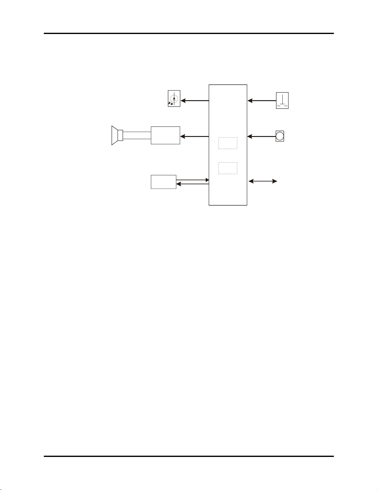
FIGURE 4-1 Trio Signal Connection Diagram (Masimo SET®)
Trio™ Service Manual 0070-10-0591-01 4 - 3

Introduction Repair Information
POW
ER
SUPPLY BOARD
0671-00-0235
NIBP MODULE0104-00-0037
ECG/R
ESP/TEMP
MODUL
E
0671-00-0239
TFT LCD DISPLAY
0160-00-0075
KE
YPA
D
0671-00-0237 or
0671-00-0064
RECORDER MODULE
0161-00-0023
1
2
3
POWER INPUT
250V/5A
1
12V
GND
5V
AC2
AC1
GND
BCON
PCO
N
SDA
SCL
KTX D
GND
5V
12V
GND
12V
GND
5V
KRX D
PLED
GND
BCON
PCON
SDA
SCL
PLED
GND
GND
KRX
D
GND
5V
GND
12V
KTX
D
12V
12V
GND
GND
12V
NRxD
NTxD
12V
ETxDERx
D
GND
12V
RRxD
RTxD
GND
RRxD
RTxD
GND
GND
12V
NRxD
NTx D
Pump
ETxD
ERxD
GND
12V
DC/DC
SHV-INLL
-INLA
-INRA
-IN
RL
EC
G CABLE ASS'Y 0012-00 1465
SHV-INLL
-INLA
-INRA
-INRLAG1T2
AG1T1
DUAL TEMP CABLE ASS'Y
SINGLE TEMP CABLE ASS'Y
AG1T2
AG1T1
1
2
FAN 011 9-00 -0197
GND
18V
3.96x3
GND
0-
2-
GND
CK+
VCC
GND
GND
2+
GND
0+
11+
VCC
CK-
/TE
5V
GND
GND
CLK
NC
DCL
K
GND
/BK
NC
PP5
PP7
DSO
GND
PP4
PP6
/RST
VCC
GND
DSI
FGND
BV-
BV+
MRST
MRST
PON
PLED
PON
PLED
2.0x8
+18V
GND
2.54x4
2.0x2
GND
SCON
SPE
AKER ASS'Y (w/cable) 0012-00-1487
GN D
SCO N
1
1
1
1
11
1
1
1
1
1
1
1
1
1
2.0x4
IBP MODULE
(OPT.)
0671-00-0241
STxD
SRxD
GND
12V
DC/DC
1
2.0x4
STxD
SRxD
GND
12V
1
1
IR
RED
I+
I-
IBP CABLE ASS'Y. 0012-00-1466
(OPT.)
B1+
B1AG
+5V
B1+
B1Vss
+5V
5V
5V
5V
GND
+18V
1
PB
1
Vbak
Vbak
GND
0-
2-
GND
CK+
VCC
GND
GND
2+
GND
0+
11+
VCC
CK-
1
BA TT
ERY
B D .
BV-
BV+
PB
2.0x8
2.54x6
2.0x6
2.54x6
2.0x6
2.54x4
2.0x3
2.54x8 2.54x8
2.0x2
2.54x2
2.0x2
2.0x5
2.
0x4
2.0x4 2.5 4x4
2.0x10x2
1.25x15
2.54x6
PE
Port
1
GND
GND
NC
NC
GND
12V
GND
5V
BRG
BACK LI GHT
HV INV ERTER
0671-00-0250
12V
GND
5V
BRG
NC
1
1
GND
A
B
S2
GAB
GND
VA B
ENCODER
A
B
S2
GAB
GND
VA B
2.0x6
2.0x 6
1
1
1
1
NETWORK
RXD-
RXD+
TXD-
TXD+
2.0x5
AGND
AGND
RXD-
RXD+
TXD-
TXD+
1
0311-00-0133
BACK LI
GHT
HV INV ERTER
0671-00-0250
HV+
HV-
HV-
HV+
0012-00-1488
0012-00-1484
0012-00-1469
0012-00-1468
0012-00-1491
0012-00-1485
0012-00-1500
0012-00-1486
0012-00-1494
(LEAD ACID)
0012-00-1478
0012-00-1477
0012-00-1493
0012-00-1499
0012-00-1481
0012-00-1490
NET INTERFACE 0012-00-1496
REDGR
EEN
COM
REDGR
EEN
GND
1
2.0x3
1
ALARM LED PC BD. 0671-00-0240
GND
NC
AOUT
1
2.54x3
1
2
ANALOG OUTPUT
(BNC)
0012-00-1497
CPU PC BD.
NELLCOR ISOLATION POWER BD.
0671-00-0247
STxD
SRxD
GND
12V
STxD
SRxD
GND
12V
DC/DC
NELLCOR
SPO PCB
0671-00-0242
or
0671-00-0066
2
NC
OGND
+12V
OGND
TX A0
123456789101112131415
VGA OUTPUT
R
G
B
H
V
0012-00-1495
GND
1
NC
0012-00-1492
1
2.0x4
1
2.0x6
NC
+5VA
RXA0
OGND
NELLCOR
MP506 SpO2 CABLE ASS'Y
OGND
+5VD
OGND
OGND
0012-00-1661
0671-00-0236 or
0671-00-0056
4 - 4 0070-10-0591-01 Trio™ Service Manual
FIGURE 4-2 Trio Signal Connection Diagram (Nellcor)

Repair Information Introduction
FIGURE 4-3 CPU PCB Connector Reference
Trio™ Service Manual 0070-10-0591-01 4 - 5

Introduction Repair Information
FIGURE 4-4 Power Supply PCB (Lead Acid Battery) Connector Reference
4 - 6 0070-10-0591-01 Trio™ Service Manual

P2
BATTERY
(LI ION)
P4
POWER/P12
POWER/P11
P5
P6
P7
FAN DISPLAY
P3
REC
Repair Information Introduction
FIGURE 4-5 Power Supply Pcb (Lithium Ion Battery) Connector Reference
Trio™ Service Manual 0070-10-0591-01 4 - 7

Introduction Repair Information
This page intentionally left blank.
4 - 8 0070-10-0591-01 Trio™ Service Manual

Repair Information Introduction
1
2
3
Power Input
250V/5A
1
GND
RRxD
RTXD
1
2
Fan 0119-00-0197
1
Charge Ass'y BD. (Li ion) 0386-00-0303
NTC
VBAT
BC
PE
Backlight HV Inverter
0671-00-0250
12V
GN
5V
BRG
NC
1
5V
12V
GND
5V
AC2
AC1
GND
BCON
PCON
SDA
SCL
PLED
BC
12V
GND
17.6V
FGND
NTC
VBAT
1
1
1
1
GND
17.6V
1
BC
Vbak
P6
12V
GND
5V
BRG
1
I
NC
NC
GND
NC
VS
NC
VBAT
NC
NC
SDA
SCL
GND
PCON
12V
5B
5V
VC
17.6V
2.54x9x2
1
17 18
17.6V
1
GND
GND
GND
Power Supply Control Bd.
0012-00-1490
Power Supply Bd. (Li Ion) 0671-00-0051
To CPU PC BD. (P12)
To CPU PC BD. (P11)
To CPU PC BD. (P13)
Recorder Module 00161-00-0023
2
P1
P2
P7
P3
P5
P4
FIGURE 4-6 Power supply board (LI Ion battery) signal connection diagram
Serial Port Converter Board P/N 0671-00-0068
J1 J2
To C PU P C
BD. (P5)
RXD
TXD
11
12V
FIGURE 4-7 Serial Port Converter board signal connection diagram
TXD
RXD
GNDGND
To S er ia l Po rt
Trio™ Service Manual 0070-10-0591-01 4 - 9

Single Temp Cable Assembly Repair Information
1
3
2
1
2
180
Te mp e ra t ur e s oc k et
1 red T1
2 black AGND
4.2 Single Temp Cable Assembly
P/N 0012-00-1468
FIGURE 4-8 Single Temp Cable Assembly
4.3 ECG Cable Assembly
P/N 0012-00-1465
FIGURE 4-9 ECG Cable Assembly
4 - 10 0070-10-0591-01 Trio™ Service Manual

Repair Information Troubleshooting
4.4 Troubleshooting
During transportation, storage and use of the Trio Monitor, various factors may result in Trio
Monitor failures or affect normal operation of the device. Some of these factors include:
Unstable network voltage, changing environmental temperature, physical damage or
component aging. During failure conditions, qualified service technicians should perform
module-level service according to the failure classification listed in the table below. Modulelevel service is defined as analysis, replacement or test of any module or modules that may
be determined defective within the device. These modules include: Power board, main
control board, TFT assembly, cable or parameter module. The repair operation must be
conducted under specific environmental conditions by a qualified service technician with
access to special test equipment.
4.4.1 Module-level Troubleshooting
Device Failures
MESSAGE/PROBLEM REASON SOLUTION
No display after power-on Blown fuse Replace fuse
Power indicator does not light Power Supply defective Replace Power Supply
Fan does not run Defective component or PCB Replace component or PCB
No display after power-on or
black screen during operation,
however, power indicator lights
on and fan runs normally
Characters are displayed
normally, however waveforms
are displayed intermittently
An operation or measurement
function is disabled
Device responds slowly Poor performance of power
Main control board failure or
display failure
Data communication error
between main control board
and parameter module
CPU PCB or corresponding
parameter PCB damage
board
Poor performance of main
control board
Poor connection of power
supply or CPU PCB
Replace CPU PCB or Display
to confirm failure
Based on error prompt,
replace CPU PCB, ribbon
cable or parameter module to
confirm failure
Examine CPU PCB and
corresponding parameter
PCB
Check power supply and
grounding system
Replace Power Supply board
Replace CPU PCB
Replace or repair connectors
Display Failures
MESSAGE/PROBLEM REASON SOLUTION
When powering on the device,
there is no display or display
goes black during normal
operation
Trio™ Service Manual 0070-10-0591-01 4 - 11
HV inverter PCB damage Connect external VGA
display to confirm the Failure,
replace HV inverter PCB
Defective display cable Repair or replace cable
Damage of CPU PCB Replace CPU PCB

Troubleshooting Repair Information
Operation, Recording
MESSAGE/PROBLEM REASON SOLUTION
Keys or Navigator™ knob
disabled
Sound is distorted or mute Keypad failure Replace keypad
Recorder will not print Recorder has no paper or roller
Record paper skews Bad recorder paper installation
Keypad or Navigator knob is
damaged
Keypad cable is damaged Replace or repair keypad
Speaker or cable failure Replace speaker or cable
lever is not pressed down
Recorder failure Replace the recorder
Recorder cable is damaged Replace or repair the
or positioning
Replace keypad or Navigator
knob
cable
Install paper and press down
the roller lever
recorder cable
Adjust the installation of
recorder paper
Power Board Failure
MESSAGE/PROBLEM REASON SOLUTION
Fuse blows upon power-on Short-circuit in power supply or
other module
Fuse blows when all loads are
disconnected
Fuse blows after connecting a
specific PCB
Indicators of power and main
control board illuminated,
however, the fan does not run
and the keypad indicator does
not illuminate
Indicators of power and main
control board do not illuminate,
however, the fan runs normally
and the keypad indicator
illuminates
Power Supply failure Replace Power Supply
PCB may be defective Replace PCB
+12V DC power is damaged Replace the power supply
+5V DC power is damaged Replace the power supply
Replace module or PCS
Check after power-on
PCB
PCB
4 - 12 0070-10-0591-01 Trio™ Service Manual

Repair Information Troubleshooting
Parameter Failure
MESSAGE/PROBLEM REASON SOLUTION
No ECG waveform Poor connection of ECG
electrodes
No square waveform exists
during CAL self-test
RL electrode is disconnected Connect RL electrode
ECG/RESP module is damaged Replace ECG/RESP module
ECG waveform interference or
abnormal ECG waveform
Electrodes are connected
incorrectly
There are disconnected or
intermittent electrodes
AC power has no grounding
plug
ECG filter mode is incorrect Select appropriate filter mode
ECG/RESP module is damaged
or defective
No RESP waveform or
abnormal RESP waveform
Electrodes are connected
incorrectly
Patient is moving constantly Keep patient calm
ECG/RESP module is damaged
or defective
TEMP value is incorrect Temp sensor is poorly
connected
HR value is inaccurate ECG waveform intermittent Check ECG connections and
NIBP cuff cannot be inflated Airway is occluded or has
leakage
Blood pressure intermittently
cannot be measured
Blood pressure measurement is
inaccurate
No SpO
SpO
waveform SpO2 Sensor or SpO2 module
2
waveform interference Patient is moving Keep the patient calm
2
Cuff becomes loose or patient is
moving
Cuff size does not fit the patient Use the appropriate size cuff
NIBP module defective Replace NIBP module
is damaged
Ambient light is very intensive Dim the ambient lighting
value is inaccurate Dye has been injected into
SpO
2
patient's body
Use new electrodes to ensure
good contact
Replace ECG/RESP module
Correctly connect electrodes
Remove any electrodes that
are not used
Use grounded power cord
and outlet
Replace ECG/RESP module
Use RA-LL
(R and F)
electrode, connect correctly
Replace ECG/RESP module
Reconnect TEMP sensor
reconnect
Adjust or repair the airway
Keep the patient calm. Rewrap the cuff correctly and
safely
Replace the sensor to confirm
the failure
Remove all dyes before
performing measurement
Trio™ Service Manual 0070-10-0591-01 4 - 13

Disassembly Instructions Repair Information
4.5 Disassembly Instructions
Before disassembling the unit, perform the following:
•Power down the unit and remove the line cord
•Remove all cable assemblies from the right side and rear of the unit
•Remove any batteries that were installed
•Perform all work on a properly grounded station
CAUTION: To ensure continued use of the Factory Defaults when the
unit is powered off and on, save the Factory Defaults as the
User Default Configuration after reassembly.
4.5.1 Tools Needed
•Phillips Screwdriver
•Slotted Screwdriver
•Awl or similar tool
4.5.2 Removal of the Front Housing
1. Remove two (2) 3 x 40 mm Phillips panhead screws at top right and left of rear housing.
2. Remove two (2) 3 x 5 mm Phillips flathead screws at front right and left of bottom
housing.
3. Carefully pull Front Housing Assembly forward and remove from rear housing.
4. Disconnect cable assemblies from connectors P3 (speaker cable assembly) and P4 (CPU
PCB to Keypad PCB cable assembly) of Keypad PCB.
4.5.3 Removal of Display
1. With Front Housing Assembly removed, place monitor face up on a flat surface.
2. Remove four (4) 2.5 x 6 mm Phillips panhead self tapping screws at corners of the 8.4"
TFT display.
3. Carefully lift display from mounting bracket.
4. Disconnect cable assembly from CN2 on the HV inverter PCB, and ribbon cable at
upper left of display.
4.5.4 Removal of Thermal Printhead Recorder
1. Open recorder door and remove paper roll, if installed.
2. Remove two (2) 3 x 6 mm Phillips panhead screws from rear of recorder paper
compartment.
3. Insert flat blade of screwdriver into tab slots at center right and center left of recorder
paper compartment.
4. Gently move tabs in toward center of paper compartment while pushing recorder out
from rear housing of unit.
4 - 14 0070-10-0591-01 Trio™ Service Manual

Repair Information Disassembly Instructions
4.5.5 Removal of PCB Chassis Assembly
1. Remove four (4) 3 x 6 mm Phillips panhead screws from rear housing.
2. Remove two (2) 4 x 10 mm Phillips panhead screws from bottom of rear housing.
3. Carefully pull entire PCB chassis assembly, along with right side parameter panel,
forward until it is completely removed from the rear housing.
4. Disconnect cable assemblies from connectors JP1 and JP3 of thermal printhead
Recorder.
4.5.6 Removal of Display Mounting Plate
1. Remove two (2) 3 x 6 mm Phillips panhead screws at left and right of HV inverter PCB.
2. Gently lift display mounting plate up from chassis assembly so that locking tabs at top of
mounting plate clear their slots.
3. Pull display mounting plate forward and away from chassis assembly.
4. Disconnect cable assemblies from P1 of CPU PCB (display cable assembly) and CN2 of
HV inverter PCB.
4.5.7 Replacement of 3V Lithium Cell Battery
1. With the display mounting plate removed, the CPU PCB is accessible. A 3volt Lithium
cell battery is installed in the battery socket at the lower center of the CPU PCB.
2. Using a small flat blade screwdriver, push the tab (located at the 7 o'clock position on
the battery holder) toward outer edge of battery socket.
3. The 3 volt lithium battery should pop out of holder. Remove and discard battery.
4. With positive (+) terminal facing up, push new 3 volt Lithium battery into battery holder
until tab locks battery in place.
4.5.8 Removal of Power Supply Assembly
1. Remove two (2) 3 x 6 mm Phillips panhead screws at front left and front center of PCB
chassis assembly.
2. Remove two (2) 3 x 6 mm Phillips panhead screws lower left side rear and lower right
side rear of PCB chassis assembly.
3. Remove cable assemblies from J2, J10, J4, J5, and J3 of Power Supply PCB.
4. Pull power supply assembly straight back from rear of PCB chassis assembly.
4.5.9 Removal of PCB Chassis Rear Panel Plate
1. Remove four (4) 3 x 6 mm Phillips panhead screws from rear panel of PCB chassis.
2. Remove rear panel plate. This will allow access to NIBP Module and optional IBP PCB.
Trio™ Service Manual 0070-10-0591-01 4 - 15

Disassembly Instructions Repair Information
4.5.10 Removal of NIBP/IBP PCB Mounting Plate
1. Remove two (2) 3 x 6 mm Phillips panhead screws at upper right side center and upper
left side center of PCB chassis assembly.
2. Remove one (1) 3 x 6 mm Phillips panhead screw at lower left of NIBP/IBP pcb
mounting plate.
3. If IBP PCB is installed, remove cable assemblies from PD1 and P2 of IBP PCB.
4. Remove cable assembly from P1 of NIBP PCB. Remove polyurethane hose from Rectus
fitting on parameter panel.
5. Lift NIBP/IBP PCB Mounting Plate up and out to remove. This will allow access to ECG/
RESP/TEMP PCB and SpO
PCB.
2
4.5.11 Removal of Handle
1. Remove two (2) 4 x 14 mm Phillips panhead self tapping screw at top inside front of
rear housing.
2. Push handle and handle shoes toward rear of rear housing until they are removed from
housing.
3. Use an awl or similar tool to push the pins through the shoes releasing the handle.
4 - 16 0070-10-0591-01 Trio™ Service Manual

Repair Information ECG Cable ESIS and Non ESIS
4.6 ECG Cable ESIS and Non ESIS
P/N 0012-00-1255-XX
-01 10’ Straight Non ESIS -05 10’ Straight ESIS
-02 20’ Straight Non ESIS -06 20’ Straight ESIS
FIGURE 4-5 ECG Cable ESIS and Non ESIS (P/N 0012-00-1255-XX)
ANSI/AAMI EC53-1995 IEC CONVENTIONAL STANDARD
LEAD COLOR LEAD COLOR
V Brown Chest (C) White
Right Arm (RA) White Right Arm (R) Red
Left Leg (LL) Red Left Leg (F) Green
Left Arm (LA) Black Left Arm (L) Ye ll ow
Right Leg (RL) Green Right Leg (N) Black
Trio™ Service Manual 0070-10-0591-01 4 - 17

ECG Shielded Lead Wires Repair Information
4.7 ECG Shielded Lead Wires
P/N 0012-00-1262-XX
-01 18" pinch 5 lead set Domestic -14 3/40" 2/60" pinch 5 lead set International
-02 24" pinch 5 lead set Domestic -07 18" pinch 3 lead set Domestic
-03 40" pinch 5 lead set Domestic -08 24" pinch 3 lead set Domestic
-04 18" pinch 5 lead set International -09 40" pinch 3 lead set Domestic
-05 24" pinch 5 lead set International -10 18" pinch 3 lead set International
-06 40" pinch 5 lead set International -11 24" pinch 3 lead set International
-13 3/40" 2/60" pinch 5 lead set Domestic -12 40" pinch 3 lead set International
FIGURE 4-6 ECG Shielded Lead Wires (P/N 0012-00-1262-XX)
4 - 18 0070-10-0591-01 Trio™ Service Manual

Repair Information ECG Shielded Lead Wires
GREEN
BLACK
RED
WHITE
BROWN
L" +/- 1.00"
GREEN
BLACK
RED
WHITE
BROWN
BLACK
YELLOW
GREEN
RED
WHITE
L" +/- 1.00"
BLACK
YELLOW
GREEN
RED
WHITE
BLACK
RED
WHITE
L" +/- 1.00"
TWO PINS
SHORTED
TWO PINS
SHORTED
KEYING BLOCKS
ARE TO BE THE SAME
COLOR AS LEAD WIRE
BLACK
RED
WHITE
YELLOW
GREEN
RED
L" +/- 1.00"
TWO PINS
SHORTED
TWO PINS
SHORTED
KEYING BLOCKS
ARE TO BE THE SAME
COLOR AS LEAD WIRE
YELLOW
GREEN
RED
LEAD
CONNECTOR
PATI EN T E ND
TERMINATION
SHIELD
P/N 0012-00-1261-XX
-01 18" snap 5 lead set Domestic -14 3/40" 2/60" snap 5 lead set International
-02 24" snap 5 lead set Domestic -07 18" snap 3 lead set Domestic
-03 40" snap 5 lead set Domestic -08 24" snap 3 lead set Domestic
-04 18" snap 5 lead set International -09 40" snap 3 lead set Domestic
-05 24" snap 5 lead set International -10 18" snap 3 lead set International
-06 40" snap 5 lead set International -11 24" snap 3 lead set International
-13 3/40" 2/60" snap 5 lead set Domestic -12 40" snap 3 lead set International
FIGURE 4-7 ECG Shielded Lead Wires (P/N 0012-00-1261-XX)
Trio™ Service Manual 0070-10-0591-01 4 - 19

Trio Wall Mounts and Rolling Stand Repair Information
Metric Panhead Screw M4X16
0211-13-0416-00
Trio Mouting Bracket Kit
0040-00-0338
4.8 Trio Wall Mounts and Rolling Stand
FIGURE 4-8 Mounting bracket kits
4 - 20 0070-10-0591-01 Trio™ Service Manual

Repair Information Trio Wall Mounts and Rolling Stand
Trio Wall Mount Kit
Trio VHM Wall Mount Kit
0040-00-0337-01
0040-00-0337-02
FIGURE 4-9 Mounting bracket kits
Trio™ Service Manual 0070-10-0591-01 4 - 21

Trio Wall Mounts and Rolling Stand Repair Information
FIGURE 4-10 Trio roll stand
Replacement Parts, Trio Rolling Stand
DESCRIPTION PART NUMBER
Trio rolling stand, value TRIOROLLSTD
Trio monitor mounting kit 0406-00-0856-01
Casters, Non locking 0401-00-0045
Casters, Locking 0401-00-0046
Utility basket 0202-00-0166
*Included in Trio Monitor Mounting Kit.
4 - 22 0070-10-0591-01 Trio™ Service Manual

5.0
Appendix
5.1 System Alarm Prompts
PROBLEM/MESSAGE REASON SOLUTION
BATTERY VOLTAGE TOO LOW When battery voltage is too
low, the monitor will
automatically shut down within
5 minutes
ECG WEAK SIGNAL The patient's ECG signal is too
weak
NO PULSE The patient's pulse signal is too
PNP The pacemaker is not paced Check the connection of the
PNC No pacemaker signal is
ECG LEAD OFF ECG lead is not connected
ECG V LEAD OFF The V lead wire of ECG is not
ECG LL LEAD OFF The LL lead wire of ECG is not
ECG LA LEAD OFF The LA lead wire of ECG is not
*XX represents all the parameter modules in the system such as ECG, NIBP, SpO
weak or non-existent
captured
correctly
connected correctly
connected correctly
connected correctly
Use AC power supply
Check if the electrodes and
lead wires are connected
correctly. Check the current
condition of the patient.
Check the connection of the
sensor. Check the current
condition of the patient.
pacemaker. Check the
connection of electrodes and
lead wires. Check the current
condition of the patient.
Check the connection of the
pacemaker. Check the
connection of electrodes and
lead wires. Check the current
condition of the patient.
Check the connection of ECG
lead wires
Check the connection of V
lead wire
Check the connection of LL
lead wire
Check the connection of LA
lead wire
, IBP module, etc.
2
Trio™ Service Manual 0070-10-0591-01 5 - 1

System Alarm Prompts Appendix
PROBLEM/MESSAGE REASON SOLUTION
ECG RA LEAD OFF The RA lead wire of ECG is not
connected correctly
ECG C LEAD OFF The C lead wire of ECG is not
connected correctly
ECG F LEAD OFF The F lead wire of ECG is not
connected correctly
ECG L LEAD OFF The L lead wire of ECG is not
connected correctly
ECG R LEAD OFF The R lead wire of ECG is not
connected correctly
SpO
SENSOR OFF SpO2 sensor is not connected
2
SpO
: INTERFERENCE Noise detected on the pulse
2
correctly
signal prevents pulse
Check the connection of RA
lead wire
Check the connection of C
lead wire
Check the connection of F
lead wire
Check the connection of L
lead wire
Check the connection of R
lead wire
Check the connection of
SpO
sensor
2
Decrease patient motion.
Check sensor.
discrimination
: PULSE SEARCH Hardware settings are being
SpO
2
adjusted in order to
discriminate a pulse waveform
Wai t seve ral secon ds for
saturation value to appear. If
it does not appear, do one of
the following:
•Change to site where
pulse is stronger if patient
is vasoconstricted
•Change or readjust
sensor if loose
: LOW PERFUSION Patient perfusion is low Check patient connection and
SpO
2
SpO
: TOO MUCH LIGHT There is too much ambient room
2
light for the sensor to function
properly
: UNRECOGNIZED
SpO
2
SENSOR
The sensor is not recognized by
the monitor
patient status
Minimize the room light
around the patient. Check
sensor.
Replace the sensor with a
recommended sensor from
Customer Service.
: COMMUNICATION
SpO
2
ERROR
The monitor and the SpO2
modules are not communicating
properly
Power the unit OFF/ON. If
problem persists, notify
hospital technician or
Customer Service.
: BOARD FAULT MasimoSET® board failed to
SpO
2
: SENSOR FAULT Defective Sensor Replace sensor
SpO
2
operate properly
TEMP SENSOR OFF TEMP sensor is not connected
correctly
IBP LEAD OFF IBP cable is not connected
correctly
ECG NOISE Excessive interference appears
on the ECG signals
Notify hospital technician or
Customer Service.
Check the connection of
TEMP sensor
Check the connection of IBP
cable
Check the connection of ECG
lead wires. Check the current
condition of the patient.
*XX ALM LMT ERR The alarm limit of XX parameter
has inadvertently deviated from
If message does not clear
contact Customer Service.
standard range
*XX represents all the parameter modules in the system such as ECG, NIBP, SpO
, IBP module, etc.
2
5 - 2 0070-10-0591-01 Trio™ Service Manual

Appendix System Alarm Prompts
PROBLEM/MESSAGE REASON SOLUTION
*XX RANGE EXCEEDED The measured value of XX
parameter has exceeded the
If message does not clear
contact Customer Service.
system measurement range
REAL CLOCK NEEDSET If the monitor displays 2000-1-
1, this system prompt reminds
the user that the current system
time is inaccurate
Reset the system time. After
setting the time, the user
should cycle power. This will
avoid any time storage
errors.
REAL CLOCK NOT EXIST The system has no cell battery
or the battery has run down
SYSTEM WD FAILURE The system has a fatal error or
SYSTEM SOFTWARE ERR
failure
SYSTEM CMOS FULL
Install or replace the cell
battery
Restart the system. If message
does not clear contact
Customer Service.
SYSTEM CMOS ERR
SYSTEM EPGA FAILURE
SYSTEM FAILURE2
SYSTEM FAILURE3
SYSTEM FAILURE4
SYSTEM FAILURE5
SYSTEM FAILURE6
SYSTEM FAILURE7
SYSTEM FAILURE8
SYSTEM FAILURE9
SYSTEM FAILURE10
SYSTEM FAILURE11
SYSTEM FAILURE12
KEYBOARD NOT AVAILABLE The keypad cannot be used Check the keys for abnormal
depression. Contact the
manufacturer for repair.
KEYBOARD COMM ERR The keypad has a failure Contact the manufacturer for
KEYBOARD ERROR
repair
KEYBOARD FAILURE
KEYBOARD ERR1
KEYBOARD ERR2
5V TOO HIGH The power supply has a failure Restart the system. If message
5V TOO LOW
POWER ERR3
does not clear contact
Customer Service.
POWER ERR4
12V TOO HIGH
12V TOO LOW
POWER ERR7
POWER ERR8
3.3V TOO HIGH
3.3V TOO LOW
*XX represents all the parameter modules in the system such as ECG, NIBP, SpO
, IBP module, etc.
2
Trio™ Service Manual 0070-10-0591-01 5 - 3

System Alarm Prompts Appendix
PROBLEM/MESSAGE REASON SOLUTION
CELL BAT TOO HIGH Cell battery is defective.
Incorrect cell battery installed
CELL BAT TOO LOW The cell battery has become
Replace the battery. If
message does not clear
contact Customer Service.
depleted. The cell battery is not
installed or the connection is
loose.
RECORDER SELF TEST ERR During the recorder self test,
there is a Recorder Module
communication failure
Execute Clear Record Task
function in the recorder setup
menu to reset communication
between the host and the
recorder. If message does not
clear contact Customer
Service.
RECORDER VLT HIGH The recorder module has
RECORDER VLT LOW
voltage failure
RECORDER HEAD HOT The continuous recording time
may be too long
Contact the manufacturer for
repair
After the recorder cools
down, use again. If the
problem still exists, contact
the manufacturer for repair.
REC HEAD IN WRONG
POSITION
The recorder roller lever is not
pressed down
Press down the recorder roller
lever
RECORDER OUT OF PAPER No paper is in the recorder Install paper into the recorder
RECORDER PAPER JAM The paper in the recorder is
jammed
RECORDER COMM ERR The communication of the
recorder is abnormal
Re-install the recorder paper
and try again
Execute Clear Record Task
from the recorder setup menu
to reset communication
between the host and the
recorder. If message does not
clear contact Customer
Service.
RECORDER PAPER W.P. The recorder paper is not
installed in the correction
Install the recorder paper in
the correct position
position
REC NOT AVAILABLE Cannot communicate with the
recorder
Execute Clear Record Task
from the recorder setup menu,
to reset communication
between the host and the
recorder. If message does not
clear contact Customer
Service.
NIBP INIT ERR NIBP initialization error Restart the system. If message
NIBP SELFTEST ERR
NIBP ILLEGALLY RESET During NIBP measurement,
illegal reset occurs
does not clear contact
Customer Service.
Check the airway of NIBP to
see if there are occlusions.
Then measure again. If the
problem persists, contact the
manufacturer for repair.
NIBP COMM ERR No NIBP communication Restart the system. If message
does not clear contact
Customer Service.
*XX represents all the parameter modules in the system such as ECG, NIBP, SpO
, IBP module, etc.
2
5 - 4 0070-10-0591-01 Trio™ Service Manual

Appendix System Alarm Prompts
PROBLEM/MESSAGE REASON SOLUTION
LOOSE CUFF The NIBP cuff is not connected
Re-connect the NIBP cuff.
correctly
AIR LEAK The NIBP cuff is not connected
correctly or there are leaks in
the airway
Check the connection of each
part or replace cuff and hose.
If message does not clear
contact Customer Service.
OVER PRESSURE NIBP is in an overpressure
condition.
Check for occlusion in cuff
and hose. Measure again. If
message does not clear
contact Customer Service.
SIGNAL SATURATED Problem occurs when
measuring NIBP. The system
cannot perform measurement,
analysis or calculation.
Check the connection of the
cuff and hose. Check
patient's condition. Measure
again, if the failure persists,
contact the manufacturer for
repair.
TIME OUT Problem occurs when
measuring NIBP. The system
cannot perform measurement,
analysis or calculation.
Check the connection of the
cuff and hose. Check
patient's condition. Measure
again, if the failure persists,
contact the manufacturer for
repair.
CUFF TYPE ERR NIBP cuff may be wrong size Check if the patient size is set
correctly. Replace existing
cuff with correct size cuff. If
the failure persists, contact
the manufacturer for repair.
PNEUMATIC LEAK NIBP airway has leaks Check the connection of cuff
and hose or replace cuff and
hose. If the failure persists,
contact the manufacturer for
repair.
MEASURE FAIL Problem occurs when
measuring NIBP. The system
cannot perform measurement,
analysis or calculation.
Check the connection of the
cuff and hose. Check
patient's condition. Measure
again, if the failure persists,
contact the manufacturer for
repair.
NIBP SYSTEM FAILURE Problem occurs when
measuring NIBP. The system
cannot perform measurement,
analysis or calculation.
Check the connection of the
cuff and hose. Check
patient's condition. Measure
again, if the failure persists,
contact the manufacturer for
repair.
*XX represents all the parameter modules in the system such as ECG, NIBP, SpO
, IBP module, etc.
2
Trio™ Service Manual 0070-10-0591-01 5 - 5

0070-10-0591-01 Revision G July 17, 2010

Mindray DS USA, Inc. • 800 MacArthur Boulevard • Mahwah, NJ 07430 • USA •
Dom. Customer Service: 1.800.288.2121 • Intl. Customer Service: +1.201.995.8000 •
Dom. Fax: 1.800.926.4275 • Intl. Fax: +1.201.995.8680 • www.mindray.com
Mindray Medical Netherlands B.V.• P.O. Box 26 • 3870 CA Hoevelaken • The Netherlands •
Tel: +3 1 33 2 5 44 91 1 • Fa x: +3 1 3 3 25 37 62 1
Mindray (UK) Limited • 3 Percy Road • St. John’s Park • Huntingdon • Cambridgeshire PE29 6SZ •
United Kingdom • Tel: 01480 416840 • Fax: 01480 436588
Mindray Medical France SARL • Europarc Créteil •123, Chemin des Bassins •
94035 Créteil Cedex • France • Tel: (0)1.45.13.91.50 • Fax: (0)1.45.13.91.51
Mindray Medical German GmbH • Zwischen den Bächen 4 • 64625 Bensheim • Germany •
Tel: +4 9. 625 1.1 7 52 4- 0 • Fa x: +4 9.62 51 .17 52 4-2 0
Mindray Medical International Ltd. • 2813 Office Tower, Convention Plaza • No 1 Harbour Road •
Wanchai • H ong Kong • Tel: +852 2793 5 596 • Fax: + 852 2344 8824
0002-08-8918
 Loading...