


Revision |
ECO# |
Approved By |
Date |
Revision History |
B |
xxxxxx |
Per ECO Approvals |
08/14/2012 |
See Last Page for Revision History |
LGD LCD Module Specification for X34
13.3” (2560X1600) TFT-LCD
THE INFORMATION CONTAINED HEREIN IS THE PROPERTY OF APPLE, INC. THE POSSESSOR AGREES TO THE FOLLOWING:
(i) TO MAINTAIN THIS DOCUMENT IN CONFIDENCE (ii) NOT TO REPRODUCE OR COPY IT (iii) NOT TO REVEAL OR PUBLISH IT IN WHOLE OR IN PART
Apple Inc. |
Size: Letter |
Scale: NONE |
Page 1 of 67 |
Title: ERIS, DSPL, LCD MODULE, LGD, X34 |
DWG Number: 069-8326 |
___Rev. B___ |
|

Revision History
Revision |
Date |
ECO |
Author |
Comments |
1 |
09/16/11 |
|
Eric Benson |
Initial Engineering Release |
2 |
12/12/11 |
|
Eric Benson |
Light Leakage and Testing Updates |
3 |
8/8/11 |
|
Eric Benson |
Optical, Mechanical, and Testing Updates |
4 |
4/24/12 |
|
Eric Benson |
Optical, Mechanical, Grinding, Electrical, Reliability |
|
|
|
|
Updates |
5 |
5/28/12 |
|
Eric Benson |
Optical, Electrical, Mechanical, Reliability Updates. |
|
|
|
|
Removed light leakage requirement |
6 |
6/7/2012 |
|
Eric Benson |
Added LCD edge ink spec. |
A |
8/06/2012 |
|
Eric Benson |
Production Release |
B |
8/14/2012 |
|
Eric Benson |
Added V-Com tuning requirement. Transmittance minimum |
|
|
|
|
updated. |
THE INFORMATION CONTAINED HEREIN IS THE PROPERTY OF APPLE, INC. THE POSSESSOR AGREES TO THE FOLLOWING:
(i) TO MAINTAIN THIS DOCUMENT IN CONFIDENCE (ii) NOT TO REPRODUCE OR COPY IT (iii) NOT TO REVEAL OR PUBLISH IT IN WHOLE OR IN PART
Apple Inc. |
Size: Letter |
Scale: NONE |
Page 2 of 67 |
Title: ERIS, DSPL, LCD MODULE, LGD, X34 |
DWG Number: 069-8326 |
___Rev. B___ |
|

TABLE OF CONTENTS |
|
|||
1. Order Of Precedence Of Documentation Authority.......................................................... |
8 |
|||
2. |
Reference Documents................................................................................................................. |
9 |
||
3. |
General Description .................................................................................................................. |
10 |
||
4. |
Functional Requirements........................................................................................................ |
11 |
||
|
4.1. |
Display Model .................................................................................................................................... |
11 |
|
|
4.2. |
Pixel Configuration .......................................................................................................................... |
12 |
|
|
4.3. |
Pixel Pitch ........................................................................................................................................... |
12 |
|
|
4.4. |
Resolution........................................................................................................................................... |
12 |
|
|
4.5. |
Rubbing Direction ............................................................................................................................ |
12 |
|
|
4.6. Interface and Driving Scheme ...................................................................................................... |
13 |
||
|
4.7. |
Front Surface Treatment................................................................................................................ |
13 |
|
5. |
Mechanical Requirements ...................................................................................................... |
13 |
||
|
5.1. Envelope Dimensions and Tolerances ...................................................................................... |
13 |
||
|
5.2. |
Active Area.......................................................................................................................................... |
13 |
|
|
5.3. |
Mass....................................................................................................................................................... |
13 |
|
|
5.4. |
Unit Flatness....................................................................................................................................... |
13 |
|
|
5.4.1. |
Flatness Measurement Requirements ................................................................................................ |
13 |
|
|
5.5. Exposed Area and Restrictions .................................................................................................... |
13 |
||
|
5.6. |
Edge Quality Requirements .......................................................................................................... |
13 |
|
|
5.6.1. |
Surface Finish Requirements.................................................................................................................. |
14 |
|
|
5.6.2. |
Edge Defect Requirements....................................................................................................................... |
15 |
|
|
5.6.3. |
Ground Surface Profile............................................................................................................................... |
16 |
|
|
5.7. |
Polarizer Edge Requirement ........................................................................................................ |
17 |
|
|
5.8. |
Mechanical Stack-up........................................................................................................................ |
18 |
|
|
5.9. Driver IC Mechanical Requirements .......................................................................................... |
18 |
||
|
5.9.1. Driver IC Edge Quality................................................................................................................................ |
18 |
||
|
5.9.2. Driver IC Top Surface Requirement..................................................................................................... |
19 |
||
|
5.10. Unit Edge Ink Requirement ........................................................................................................ |
19 |
||
6. |
Thermal Requirements............................................................................................................ |
19 |
||
7. |
Electrical Requirements .......................................................................................................... |
19 |
||
|
7.1. |
Block Diagram ................................................................................................................................... |
19 |
|
|
7.2. |
Display PCB Schematics.................................................................................................................. |
20 |
|
|
7.3. |
Display PCB Layout .......................................................................................................................... |
21 |
|
|
7.4. |
Active Components .......................................................................................................................... |
21 |
|
|
7.4.1. |
Electrical Interface Requirements........................................................................................................ |
21 |
|
|
7.4.2. Extended Display Identification Data (EDID) Interface .............................................................. |
22 |
||
|
7.4.3. |
Power Supply Requirements .................................................................................................................. |
25 |
|
|
7.4.4. |
Signal Timing ................................................................................................................................................. |
25 |
|
|
7.4.5. Power Requirements (W/O backlight)............................................................................................... |
27 |
||
|
7.4.6. |
Display Pattern Requirements ............................................................................................................... |
27 |
|
|
7.5. |
Power on-off sequence ................................................................................................................... |
28 |
|
|
7.6. Vcc Voltage Drop Requirement.................................................................................................... |
28 |
||
|
7.7. |
Near-Field Noise................................................................................................................................ |
28 |
|
|
7.8. eDP Bit-Error-Rate (BER) Requirement ................................................................................... |
28 |
||
|
7.9. COG Bit Error Rate (BER) Requirement.................................................................................... |
28 |
||
|
7.10. |
Programmable Gamma Settings ............................................................................................... |
28 |
|
THE INFORMATION CONTAINED HEREIN IS THE PROPERTY OF APPLE, INC. THE POSSESSOR AGREES TO THE FOLLOWING:
(i) TO MAINTAIN THIS DOCUMENT IN CONFIDENCE (ii) NOT TO REPRODUCE OR COPY IT (iii) NOT TO REVEAL OR PUBLISH IT IN WHOLE OR IN PART
Apple Inc. |
Size: Letter |
Scale: NONE |
Page 3 of 67 |
Title: ERIS, DSPL, LCD MODULE, LGD, X34 |
DWG Number: 069-8326 |
___Rev. B___ |
|

|
7.11. |
Backlight Subsystem..................................................................................................................... |
29 |
|
|
7.11.1. |
General Information................................................................................................................................. |
29 |
|
|
7.11.2. |
Backlight Electrical Characteristics................................................................................................... |
29 |
|
|
7.11.3. |
LED Connection.......................................................................................................................................... |
31 |
|
|
7.11.4. LED string to string current variation.............................................................................................. |
32 |
||
|
7.11.5. |
LED Driver Requirement........................................................................................................................ |
32 |
|
|
7.12. |
ITO Electrical Shielding................................................................................................................ |
32 |
|
8. |
Optical Requirements............................................................................................................... |
34 |
||
|
8.1. |
General Optical Specifications ..................................................................................................... |
34 |
|
|
8.2. |
Optical Measuring Conditions...................................................................................................... |
35 |
|
|
8.2.1. |
Center Point Luminance............................................................................................................................ |
36 |
|
|
8.2.2. |
Average Luminance..................................................................................................................................... |
37 |
|
|
8.2.3. |
Brightness Uniformity................................................................................................................................ |
37 |
|
|
8.2.4. |
Contrast Ratio................................................................................................................................................ |
37 |
|
|
8.2.5. |
White Color Uniformity............................................................................................................................. |
37 |
|
|
8.2.6. Panel to Panel White Color Uniformity .............................................................................................. |
38 |
||
|
8.2.7. Max Color Difference with respect to the center within a panel............................................. |
38 |
||
|
8.2.8. Max Color Difference between any two points within the panel ............................................ |
38 |
||
|
8.2.9. Average Color Difference between top and bottom...................................................................... |
38 |
||
|
8.2.10. Max Color Difference between two neighbors ............................................................................. |
39 |
||
|
8.2.11. |
RGB Color Chromaticity.......................................................................................................................... |
39 |
|
|
8.2.12. |
Viewing Angle ............................................................................................................................................. |
39 |
|
|
8.2.13. |
Gray Scale Inversion................................................................................................................................. |
39 |
|
|
8.2.14. |
Response Time ........................................................................................................................................... |
40 |
|
|
8.2.15. Gray Scale Linearity or Gamma Value .............................................................................................. |
41 |
||
|
8.3. |
Flicker................................................................................................................................................... |
41 |
|
|
8.4. |
Cross-talk ............................................................................................................................................ |
41 |
|
|
8.5. |
Surface Reflection............................................................................................................................. |
42 |
|
|
8.6. General Requirement for Camera and CIL/ALS Area ........................................................... |
43 |
||
|
8.7. Camera/ALS/CIL Optical Parameter Definition..................................................................... |
44 |
||
|
8.7.1. |
Camera Window Transmittance............................................................................................................ |
44 |
|
|
8.7.2. |
Camera Window Parallelism................................................................................................................... |
44 |
|
|
8.7.3. Camera Window Transmitted Wavefront Distortion................................................................... |
44 |
||
|
8.7.4. |
Haze.................................................................................................................................................................... |
44 |
|
|
8.7.5. |
Color Shift........................................................................................................................................................ |
44 |
|
|
8.7.6. ALS and CIL Transmittance ..................................................................................................................... |
44 |
||
|
8.8. |
Image Retention................................................................................................................................ |
45 |
|
|
8.8.1. Quick Check Image Retention................................................................................................................. |
46 |
||
|
8.8.2. Short Term Image Retention................................................................................................................... |
46 |
||
|
8.8.3. |
Middle Term................................................................................................................................................... |
46 |
|
|
8.8.4. |
Long Term....................................................................................................................................................... |
46 |
|
|
8.9. Common Voltage (Vcom) Tuning Requirements ................................................................... |
46 |
||
|
8.10. |
Color Washout................................................................................................................................. |
47 |
|
|
8.10.1. Testing Method and Condition ............................................................................................................ |
47 |
||
|
8.10.2. Observation and Pass Criteria ............................................................................................................. |
48 |
||
|
8.11. ODF Fill Amount and Suction Cup Testing............................................................................. |
48 |
||
|
8.12. |
FOS Shimmering Specifications................................................................................................. |
48 |
|
9. |
ENVIRONMENTAL....................................................................................................................... |
49 |
||
|
9.1. |
Shock Requirements........................................................................................................................ |
49 |
|
|
9.2. |
Sine Vibration Requirements....................................................................................................... |
49 |
|
THE INFORMATION CONTAINED HEREIN IS THE PROPERTY OF APPLE, INC. THE POSSESSOR AGREES TO THE FOLLOWING:
(i) TO MAINTAIN THIS DOCUMENT IN CONFIDENCE (ii) NOT TO REPRODUCE OR COPY IT (iii) NOT TO REVEAL OR PUBLISH IT IN WHOLE OR IN PART
Apple Inc. |
Size: Letter |
Scale: NONE |
Page 4 of 67 |
Title: ERIS, DSPL, LCD MODULE, LGD, X34 |
DWG Number: 069-8326 |
___Rev. B___ |
|

9.3. |
Temperature and Humidity.......................................................................................................... |
49 |
||
9.4. |
Non-operational Environmental Requirements.................................................................... |
49 |
||
|
9.4.1. |
Low Temperature ........................................................................................................................................ |
49 |
|
|
9.4.2. |
High Temperature ....................................................................................................................................... |
49 |
|
|
9.4.3. High Temperature and High Humidity............................................................................................... |
50 |
||
|
9.4.4. |
Thermal Shock............................................................................................................................................... |
50 |
|
9.5. |
Operational Testing......................................................................................................................... |
50 |
||
|
9.5.1. |
Low Temperature ........................................................................................................................................ |
50 |
|
|
9.5.2. |
High Temperature ....................................................................................................................................... |
50 |
|
|
9.5.3. |
Heat Soak......................................................................................................................................................... |
50 |
|
|
9.5.4. High Temperature and High Humidity............................................................................................... |
50 |
||
|
9.5.5. Four Corner Test (72 hrs – operating) ............................................................................................... |
50 |
||
9.6. |
Altitude ................................................................................................................................................ |
50 |
||
9.7. |
Cold Soak ............................................................................................................................................. |
50 |
||
10. |
FREQUENCY MARGIN.............................................................................................................. |
51 |
||
11. |
RELIABILITY.............................................................................................................................. |
52 |
||
11.1. |
4-Corner Peeling Test (Color Filter (CF) & TFT)................................................................. |
52 |
||
|
11.1.1. 4-Corner Peel Test Procedure.............................................................................................................. |
53 |
||
11.2. LCD Assembly Ball-on-Ring Test............................................................................................... |
53 |
|||
|
11.2.1. |
BOR Test Configuration.......................................................................................................................... |
54 |
|
|
11.2.2. |
BOR Test Procedure................................................................................................................................. |
55 |
|
11.3. LCD Assembly 4-Point Bend Test.............................................................................................. |
56 |
|||
|
11.3.1. 4-Point Bend Test Setup......................................................................................................................... |
56 |
||
|
11.3.2. 4-Point Bend Test Procedure............................................................................................................... |
58 |
||
11.4. Polarizer Perimeter Delamination Test................................................................................. |
60 |
|||
11.5. LCD Display Column Spacer Test .............................................................................................. |
60 |
|||
11.6. Flexible Printed Circuit (FPC) Strain Relief .......................................................................... |
61 |
|||
11.7. Rigid Flex Bending Tests ............................................................................................................. |
61 |
|||
11.8. Flex Cable to Glass Bonding Strength...................................................................................... |
62 |
|||
11.9. |
Spacer Rigidity Testing ................................................................................................................ |
62 |
||
11.10. Shielding ITO Sheet Resistance Heat Soak.......................................................................... |
63 |
|||
11.11. Electrostatic Discharge (ESD) Test........................................................................................ |
64 |
|||
11.12. |
MTBF................................................................................................................................................ |
64 |
||
12. |
COSMETIC REQUIREMENTS.................................................................................................. |
65 |
||
13. DISPLAY SERIAL NUMBERS AND LABELING.................................................................... |
65 |
|||
14. |
REGULATORY ............................................................................................................................ |
65 |
||
14.1. Product Safety (Environmental, Ergonomics, Safety and Health)................................. |
65 |
|||
14.2. RoHS Compliance and other Substance Regulations ......................................................... |
65 |
|||
14.3. |
Halogen Free.................................................................................................................................... |
66 |
||
14.4. Environmental Markings and Recycling ................................................................................ |
66 |
|||
14.5. |
Product Safety ................................................................................................................................. |
66 |
||
14.6. |
Ergonomics ...................................................................................................................................... |
66 |
||
14.7. |
Electromagnetic Compatibility (EMC) .................................................................................... |
66 |
||
|
14.7.1. |
Electromagnetic Emissions Requirements .................................................................................... |
66 |
|
|
14.7.2. |
Electromagnetic Immunity Requirements..................................................................................... |
66 |
|
15. |
14.7.3. |
EMC Production Audit Procedure...................................................................................................... |
66 |
|
|
Acronyms.................................................................................................................................... |
67 |
||
THE INFORMATION CONTAINED HEREIN IS THE PROPERTY OF APPLE, INC. THE POSSESSOR AGREES TO THE FOLLOWING:
(i) TO MAINTAIN THIS DOCUMENT IN CONFIDENCE (ii) NOT TO REPRODUCE OR COPY IT (iii) NOT TO REVEAL OR PUBLISH IT IN WHOLE OR IN PART
Apple Inc. |
Size: Letter |
Scale: NONE |
Page 5 of 67 |
Title: ERIS, DSPL, LCD MODULE, LGD, X34 |
DWG Number: 069-8326 |
___Rev. B___ |
|

Table of Figures
FIGURE 1 LCD ASSEMBLY OVERVIEW |
10 |
FIGURE 2 RESOLUTION OVERVIEW |
12 |
FIGURE 3 RUBBING DIRECTIONS |
12 |
FIGURE 4 SURFACE ROUGHNESS MEASUREMENT AREA |
14 |
FIGURE 5 SURFACE ROUGHNESS MEASUREMENT TEST CONFIGURATIONS |
14 |
FIGURE 6 GRINDING ZONE DEFINITIONS |
16 |
FIGURE 7 GLASS CHIP PROFILE DEFINITION |
16 |
FIGURE 8 CHAMFER OF GRINDING EDGE PROFILE |
17 |
FIGURE 9 GRINDING PROFILE ZONE DEFINITIONS |
17 |
FIGURE 10 POLARIZER OVERHANG REQUIREMENT |
18 |
FIGURE 11 DRIVER IC EDGE QUALITY |
19 |
FIGURE 12 UNIT ELECTRICAL BLOCK DIAGRAM (FOR REFERENCE ONLY) |
20 |
FIGURE 13 CONNECTOR DRAWING (PCB SIDE) |
21 |
FIGURE 14 WHITE SCREEN DISPLAY FIGURE 15 MOSAIC PATTERN DISPLAY |
28 |
FIGURE 16 VERTICAL STRIPE PATTERN DISPLAY |
28 |
FIGURE 17 LED CONTROLLER BLOCK DIAGRAM |
30 |
FIGURE 18 LED CONTROLLER REFERENCE APPLICATION CIRCUITS |
30 |
FIGURE 19 DISPLAY BACKLIGHT CONTROL DIAGRAM |
31 |
FIGURE 20 ITO TRANSMITTANCE |
33 |
FIGURE 21 OPTICAL MEASUREMENT SET-UP |
36 |
FIGURE 22 OPTICAL MEASUREMENT POINTS |
36 |
FIGURE 23 NEIGHBORING POINTS |
37 |
FIGURE 24 VIEWING ANGLE DEFINITION |
39 |
FIGURE 25 RESPONSE TIME MEASUREMENT |
40 |
FIGURE 26 GRAY TO GRAY RESPONSE TIME |
41 |
FIGURE 27 CROSS TALK MEASUREMENT |
42 |
FIGURE 28 SURFACE REFLECTION MEASUREMENT |
43 |
FIGURE 29 CAMERA/ALS/CIL PATTERN MEASUREMENT |
45 |
FIGURE 30 IMAGE RETENTION CHECKING CONDITION |
45 |
FIGURE 31 IMAGE RETENTION CHECKING PATTERNS |
46 |
FIGURE 32 COLOR WASHOUT TEST LOCATIONS |
47 |
FIGURE 33 4-CORNER PEEL TEST SETUP |
52 |
FIGURE 34 4-CORNER PEEL TEST EXAMPLE |
53 |
FIGURE 35 BALL AND SUPPORT RING GEOMETRY |
54 |
FIGURE 36 EXAMPLE OF BALL ON RING TEST CONFIGURATION (INSTRON) |
55 |
FIGURE 37 MODULE TEST LOCATIONS FOR BALL ON RING TEST |
55 |
FIGURE 38 4 POINT BEND 90% SURVIVAL RATE ON WEIBULL PROBABILITY PLOT |
56 |
FIGURE 394 POINT BEND TEST SETUP |
57 |
FIGURE 40 4-POINT BEND HORIZONTAL GLASS CONFIGURATION |
57 |
FIGURE 41 4-POINT BEND VERTICAL GLASS CONFIGURATION |
58 |
FIGURE 42 4-POINT BEND FAILURE CASE OVERVIEW |
59 |
FIGURE 43 STRAIN RELIEF ON THE FPC |
61 |
FIGURE 44 FPC LEVEL BENDING TEST |
62 |
FIGURE 45 FISHERSCOPE HM2000 |
63 |
FIGURE 46 SPACER RIGIDITY TEST |
63 |
THE INFORMATION CONTAINED HEREIN IS THE PROPERTY OF APPLE, INC. THE POSSESSOR AGREES TO THE FOLLOWING:
(i) TO MAINTAIN THIS DOCUMENT IN CONFIDENCE (ii) NOT TO REPRODUCE OR COPY IT (iii) NOT TO REVEAL OR PUBLISH IT IN WHOLE OR IN PART
Apple Inc. |
Size: Letter |
Scale: NONE |
Page 6 of 67 |
Title: ERIS, DSPL, LCD MODULE, LGD, X34 |
DWG Number: 069-8326 |
___Rev. B___ |
|

Table of Tables
TABLE 1 UNIFIED DISPLAY FOR X34 GENERAL DESCRIPTION |
11 |
TABLE 2 DISPLAY SUBSYSTEM CONNECTOR PIN ASSIGNMENT (FOR REFERENCE ONLY) |
22 |
TABLE 3 EDID DATA (FOR REFERENCE ONLY) |
23 |
TABLE 4 COLOR DATA REFERENCE |
26 |
TABLE 5 LED REQUIREMENTS (CHARACTERIZED AT 20 MA) |
29 |
TABLE 6 LED CONNECTION DATA |
31 |
TABLE 7 LED CONNECTOR ASSIGNMENTS (FOR REFERENCE ONLY) |
31 |
TABLE 8 ITO LAYER CHARACTERISTICS |
32 |
TABLE 9 GENERAL OPTICAL CHARACTERISTICS |
34 |
TABLE 10 CAMERA AND CIL/ALS REQUIREMENTS |
43 |
TABLE 11 COLOR WASHOUT TEST CONDITIONS |
47 |
TABLE 12 APPLE DEVELOPMENT DISPLAY LABEL REQUIREMENTS |
65 |
THE INFORMATION CONTAINED HEREIN IS THE PROPERTY OF APPLE, INC. THE POSSESSOR AGREES TO THE FOLLOWING:
(i) TO MAINTAIN THIS DOCUMENT IN CONFIDENCE (ii) NOT TO REPRODUCE OR COPY IT (iii) NOT TO REVEAL OR PUBLISH IT IN WHOLE OR IN PART
Apple Inc. |
Size: Letter |
Scale: NONE |
Page 7 of 67 |
Title: ERIS, DSPL, LCD MODULE, LGD, X34 |
DWG Number: 069-8326 |
___Rev. B___ |
|

1. Order Of Precedence Of Documentation Authority
In the case of any conflict in any specification related to these parts, this order of precedence of authority shall apply:
•The Purchase Order
•This Specification
•Reference Documents
THE INFORMATION CONTAINED HEREIN IS THE PROPERTY OF APPLE, INC. THE POSSESSOR AGREES TO THE FOLLOWING:
(i) TO MAINTAIN THIS DOCUMENT IN CONFIDENCE (ii) NOT TO REPRODUCE OR COPY IT (iii) NOT TO REVEAL OR PUBLISH IT IN WHOLE OR IN PART
Apple Inc. |
Size: Letter |
Scale: NONE |
Page 8 of 67 |
Title: ERIS, DSPL, LCD MODULE, LGD, X34 |
DWG Number: 069-8326 |
___Rev. B___ |
|

2. Reference Documents
NUMBER |
TITLE |
|
069-7821 |
LCD, MCO, X34 |
|
070-1191 |
Supplier Quality and Business Requirements, Apple |
|
070-0385 |
Apple Service Requirements |
|
069-7366 |
LCD Engineering Cosmetic Specification |
|
069-7370 |
X34 Unified Backlight Specification |
|
080-0855 |
Drop, Shock and Vibration |
|
080-0854 |
Four-Corner Temperature and Humidity Test |
|
062-0087 |
Packaging Finished Goods Shock and Vibration |
|
062-7993 |
Electromagnetic Emissions Requirements |
|
062-7994 |
Electromagnetic Immunity Requirements |
|
080-0840 |
EMC Production Audit Procedure |
|
062-2082 |
Vendor Packaging Procedure |
|
062-0585 |
FG Labeling Specification |
|
062-2111 |
Manufacturing Bar Code Specification |
|
062-2208 |
Static Breakage Test |
|
070-0371 |
Service: Packaging Standard |
|
070-0385 |
Service: Product Quality Requirements |
|
070-1191 |
Supplier Quality and Business Requirement |
|
070-1193 |
Barcode Label Specification |
|
074-0321 |
ESD Anti-static Label Specification |
|
13406-2.3 |
ISO Specification |
|
062-0093 |
Apple Corporate Specification, Mandatory Requirements for Product Safety |
|
IEC60950 |
Safety of Information Technology Equipment (International Standard) |
|
EN 60950 |
Safety of Information Technology Equipment (European Standard based on |
|
IEC 60950) |
||
|
||
|
Safety of Information Technology Equipment . Third Edition (US Standard |
|
UL 1950 |
based on IEC 60950) C22.2 No. 950 Safety of Information Technology |
|
|
Equipment. Third Edition (Canadian Standard based on IEC 60950) |
|
|
Tests for Flammability of Plastic Materials for Parts in Devices and |
|
UL 94 |
Appliances (UL standard for flame testing plastics. Includes test |
|
|
requirements for HB, V-2, V-1 and V-0 flame ratings) |
|
JIS K 5401 |
Pencil Scratch Tester for Coated Film 13406-2.3 |
|
069-0279 |
Product Safety Requirements for Component Flat Panel Display Assemblies |
|
069-1111 |
Apple RoHS Compliance Specification |
|
080-2153 |
Apple’s RoHS Declaration of Conformity Procedure |
THE INFORMATION CONTAINED HEREIN IS THE PROPERTY OF APPLE, INC. THE POSSESSOR AGREES TO THE FOLLOWING:
(i) TO MAINTAIN THIS DOCUMENT IN CONFIDENCE (ii) NOT TO REPRODUCE OR COPY IT (iii) NOT TO REVEAL OR PUBLISH IT IN WHOLE OR IN PART
Apple Inc. |
Size: Letter |
Scale: NONE |
Page 9 of 67 |
Title: ERIS, DSPL, LCD MODULE, LGD, X34 |
DWG Number: 069-8326 |
___Rev. B___ |
|
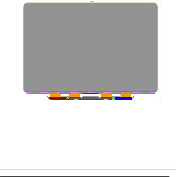
3. General Description
The board assembly drawing for X34 is shown in Figure 1. The LCD Module contains the following hardware. From this point forward the complete Unified Display for X34 13.3” TFT-LCD will be referred to as the unit.
•2x 0.3 mm glass (TFT and CF)
•Liquid Crystal
•Front and Rear Polarizers
•IC Drivers on glass
•PCB with rigid flex cables
•COG Spacer
•ITO Tape
•PCB Label / Insulation Tape
Figure 1 LCD Assembly Overview
THE INFORMATION CONTAINED HEREIN IS THE PROPERTY OF APPLE, INC. THE POSSESSOR AGREES TO THE FOLLOWING:
(i) TO MAINTAIN THIS DOCUMENT IN CONFIDENCE (ii) NOT TO REPRODUCE OR COPY IT (iii) NOT TO REVEAL OR PUBLISH IT IN WHOLE OR IN PART
Apple Inc. |
Size: Letter |
Scale: NONE |
Page 10 of 67 |
Title: ERIS, DSPL, LCD MODULE, LGD, X34 |
DWG Number: 069-8326 |
___Rev. B___ |
|
4. Functional Requirements
Table 1 provides a summary of the functionality and requirements of the LCD Module.
|
Table 1 Unified Display for X34 General Description |
|
||
Category |
Parameter |
Specification |
Reference |
|
Section |
||||
|
|
|
||
General |
LCD TYPE |
Normally-Black Transmissive, Mobile-IPS a-SI TFT-LCD |
4.1 |
|
|
Product Code |
TBA |
N/A |
|
|
Manufacturer |
LGD |
N/A |
|
|
Manufacturer P/N |
TBD |
N/A |
|
|
Diagonal |
13.3” |
|
|
|
Pixel Format |
2560 (RGB stripe, H) x 1600 (V) |
4.4 |
|
|
Pixel Pitch |
0.03725(V) x 3 x 0.11175(H) mm |
4.3 |
|
|
Color Depth |
24-bits (8R, 8G, 8B) |
|
|
|
Packaging |
Protective film on front & back polarizer w/ pull tab. LCD |
|
|
|
|
board packaged and sealed in ESD protection bags in class |
|
|
|
|
10k or better clean room with all the glass edge & flex/ PCB |
|
|
Electrical |
|
protections |
|
|
Interface |
5V input power, 4 lane DisplayPort interface |
7.4.3 |
||
|
Power |
2.0W Typical (Web Black/White/Mosaic) |
7.4.5 |
|
|
Consumption |
2.6W Worse Case (R/G/B) |
|
|
|
Inversion |
Z-inversion (1-dot) |
4.6 |
|
|
Color Filter ITO |
2.0 kΩ / square typical |
7.12 |
|
Mechanical |
Sheet Resistance |
2.5 kΩ / square maximum |
|
|
Active Area |
286.08 mm (H) X 178.80 mm (V) |
5.2 |
||
|
Minimum Viewing |
354.11 mm x 231.70 mm |
|
|
|
Area |
|
|
|
|
Module Outline |
354.49 mm x 237.30 mm |
5.1 |
|
|
Size |
|
|
|
|
LCD Panel |
iPEX:CAB CA 30 pins: 20525-130E-02 |
7.4.1 |
|
|
Receptacle |
|
|
|
|
Cable Plug |
iPEX:CAB CA 30 pins: 20523-130T-01 |
7.4.1 |
|
|
Perimeter Flatness |
0.3 mm |
|
|
|
Vertical Bending |
-5 to 15 |
|
|
|
Mass |
125 (typical), max 130 g |
5.3 |
|
Environmental |
Operating |
0°C to +60°C |
9.5 |
|
|
Temperature |
|
|
|
|
(functioning) |
25 +/- 3 0C and 60% +/- 5% relative humidity to maintain |
|
|
|
Storage |
|
||
|
Temperature |
panel flatness |
|
|
4.1.Display Model
The unit shall be Normally-Black, Transmissive, Mobile-IPS a-SI TFT-LCD with compensation film polarizer.
THE INFORMATION CONTAINED HEREIN IS THE PROPERTY OF APPLE, INC. THE POSSESSOR AGREES TO THE FOLLOWING:
(i) TO MAINTAIN THIS DOCUMENT IN CONFIDENCE (ii) NOT TO REPRODUCE OR COPY IT (iii) NOT TO REVEAL OR PUBLISH IT IN WHOLE OR IN PART
Apple Inc. |
Size: Letter |
Scale: NONE |
Page 11 of 67 |
Title: ERIS, DSPL, LCD MODULE, LGD, X34 |
DWG Number: 069-8326 |
___Rev. B___ |
|

4.2.Pixel Configuration
The unit shall be configured using a RGB Vertical Stripe, Vertical Chevron Dual Domain.
4.3.Pixel Pitch
The unit shall provide a sub pixel pitch no greater than 0.03725 mm x 0.11175 mm
4.4.Resolution
The unit shall be no less than 2560 (RGB stripe, H) x 1600 (V).
Figure 2 Resolution Overview
4.5.Rubbing Direction
The unit shall have Color Filter (CF) Rubbing from the bottom of the module to the top and shall have TFT Rubbing from the top of the module to the bottom as shown in Figure 3.
Figure 3 Rubbing Directions
THE INFORMATION CONTAINED HEREIN IS THE PROPERTY OF APPLE, INC. THE POSSESSOR AGREES TO THE FOLLOWING:
(i) TO MAINTAIN THIS DOCUMENT IN CONFIDENCE (ii) NOT TO REPRODUCE OR COPY IT (iii) NOT TO REVEAL OR PUBLISH IT IN WHOLE OR IN PART
Apple Inc. |
Size: Letter |
Scale: NONE |
Page 12 of 67 |
Title: ERIS, DSPL, LCD MODULE, LGD, X34 |
DWG Number: 069-8326 |
___Rev. B___ |
|

4.6.Interface and Driving Scheme
The unit shall provide a 5V 4-lane DisplayPort interface, requiring Hsync and Vsync signals, along with DE (Data Enable) mode, 1-dot Z-inversion scheme.
4.7.Front Surface Treatment
The front surface of the unit shall provide a Dry AR1.5 coating that meets the requirements specified herein.
5. Mechanical Requirements
5.1.Envelope Dimensions and Tolerances
The unit shall meet the dimensional requirements specified in 069-7821 LCD, MCO, X34.
5.2.Active Area
The unit shall meet the active area requirement specified in 069-7821 LCD, MCO, X34.
5.3.Mass
The unit mass shall not exceed the mass specified in 069-7821 LCD, MCO, X34.
5.4.Unit Flatness
The LCD module shall meet the flatness requirement specified in 069-7821 LCD, MCO, X34.
5.4.1. Flatness Measurement Requirements
All units shall require a flatness measurement after aging that meet the following requirements:
•Flatness measurement shall be completed within 24 hours after removal from aging chamber
•Post aging, unit shall be stored in 25 +/- 3 0C and 60% +/- 5% relative humidity
5.5.Exposed Area and Restrictions
The display module shall not have exposed edges or components, which may cause injury or damage during handling, inspection, assembly, and service. Exposed areas of the display module (those not protected or shielded by construction) must be insulated and otherwise protected to eliminate the possibility of electrical shorting or destructive ESD discharges (per Section 7.2) during handling, inspection, assembly, and service.
5.6.Edge Quality Requirements
The edge quality of the module shall be measured using an optical profiler such as the Keyence VK-9700 or equivalent.
THE INFORMATION CONTAINED HEREIN IS THE PROPERTY OF APPLE, INC. THE POSSESSOR AGREES TO THE FOLLOWING:
(i) TO MAINTAIN THIS DOCUMENT IN CONFIDENCE (ii) NOT TO REPRODUCE OR COPY IT (iii) NOT TO REVEAL OR PUBLISH IT IN WHOLE OR IN PART
Apple Inc. |
Size: Letter |
Scale: NONE |
Page 13 of 67 |
Title: ERIS, DSPL, LCD MODULE, LGD, X34 |
DWG Number: 069-8326 |
___Rev. B___ |
|
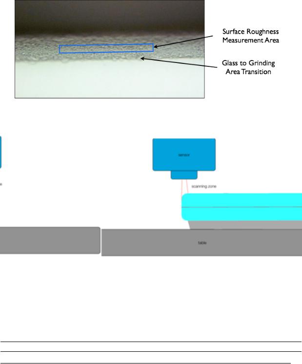
5.6.1.Surface Finish Requirements
5.6.1.1.Measurement Requirements
The following settings on the Keyence VK-9700 shall be used to measure the surface finish requirements.
•20x Objective
•Measurement Area: 0.25 mm x 0.1 mm
•Measurement Area distance from Glass Grinding Transition: 0.015 mm
Figure 4 Surface Roughness Measurement Area
Figure 5 Surface Roughness Measurement Test Configurations
5.6.1.2.Root Mean Square (Rq)
The ground edge surface Root Mean Square shall not exceed 2.25 um.
THE INFORMATION CONTAINED HEREIN IS THE PROPERTY OF APPLE, INC. THE POSSESSOR AGREES TO THE FOLLOWING:
(i) TO MAINTAIN THIS DOCUMENT IN CONFIDENCE (ii) NOT TO REPRODUCE OR COPY IT (iii) NOT TO REVEAL OR PUBLISH IT IN WHOLE OR IN PART
Apple Inc. |
Size: Letter |
Scale: NONE |
Page 14 of 67 |
Title: ERIS, DSPL, LCD MODULE, LGD, X34 |
DWG Number: 069-8326 |
___Rev. B___ |
|
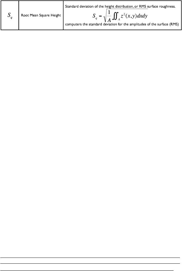
Root Mean Square is defined as:
5.6.1.3.Maximum Height (Rz_max)
The ground edge Maximum Height shall not exceed 25 um where maximum height is defined as distance between the highest peak and the lowest valley.
5.6.2. Edge Defect Requirements
The module shall have an edge scan completed using the Meere Company X35 EDGE INSPECTION SYSTEM Model No. EI-AGTT-17.3.
The ground edge surface shall not exceed the following chip size requirements as specified for each grinding zone (see Figure 6).
•Zone 1: CF/TFT Glass Perimeter (0.6t)
o0 defects greater than 50 um in any direction
•Zone 2: Bottom TFT Ledge (0.3t)
o0 defects greater than 50 um in any direction
•Zone 3: CF Edge (Scribe / Break)
oX-Dimension: Defect shall not exceed 500 um
oY-Dimension: Defect shall not exceed 500 um
•Zone 4: Bottom TFT Corners (0.3t)
oX- Dimension: No defect length requirement
o Y-Dimension: Defect shall not exceed 150 um
THE INFORMATION CONTAINED HEREIN IS THE PROPERTY OF APPLE, INC. THE POSSESSOR AGREES TO THE FOLLOWING:
(i) TO MAINTAIN THIS DOCUMENT IN CONFIDENCE (ii) NOT TO REPRODUCE OR COPY IT (iii) NOT TO REVEAL OR PUBLISH IT IN WHOLE OR IN PART
Apple Inc. |
Size: Letter |
Scale: NONE |
Page 15 of 67 |
Title: ERIS, DSPL, LCD MODULE, LGD, X34 |
DWG Number: 069-8326 |
___Rev. B___ |
|
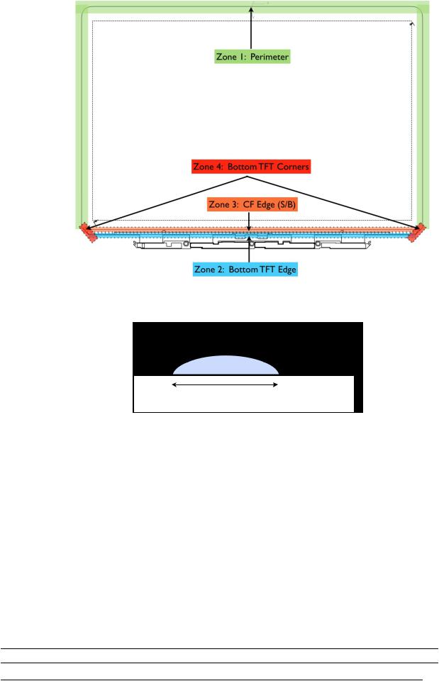
Figure 6 Grinding Zone Definitions
Glass Chip
Y-Dimension
X-Dimension
Figure 7 Glass Chip Profile Definition
5.6.3. Ground Surface Profile
The top and bottom chamfer size (Figure 8) of the glass shall meet the following requirements shown below in the specified zone (Figure 9):
•Zone 1: CF/TFT Glass Perimeter (0.6t): o 200 um ≥ chamfer size ≥ 60 um
•Zone 2: Bottom TFT Ledge (0.3t)
o 200 um ≥ chamfer size ≥ 50 um
THE INFORMATION CONTAINED HEREIN IS THE PROPERTY OF APPLE, INC. THE POSSESSOR AGREES TO THE FOLLOWING:
(i) TO MAINTAIN THIS DOCUMENT IN CONFIDENCE (ii) NOT TO REPRODUCE OR COPY IT (iii) NOT TO REVEAL OR PUBLISH IT IN WHOLE OR IN PART
Apple Inc. |
Size: Letter |
Scale: NONE |
Page 16 of 67 |
Title: ERIS, DSPL, LCD MODULE, LGD, X34 |
DWG Number: 069-8326 |
___Rev. B___ |
|
Figure 8 Chamfer of grinding edge profile
Figure 9 Grinding Profile Zone Definitions
5.7.Polarizer Edge Requirement
The laser cut polarizer edge with release lines removed shall be inspected using a variable pressure electron microscope to evaluate polarizer edge damage.
Polarizer overhang on the edge of the polarizer caused from laser cutting shall not exceed 15 um as shown in Figure 10.
THE INFORMATION CONTAINED HEREIN IS THE PROPERTY OF APPLE, INC. THE POSSESSOR AGREES TO THE FOLLOWING:
(i) TO MAINTAIN THIS DOCUMENT IN CONFIDENCE (ii) NOT TO REPRODUCE OR COPY IT (iii) NOT TO REVEAL OR PUBLISH IT IN WHOLE OR IN PART
Apple Inc. |
Size: Letter |
Scale: NONE |
Page 17 of 67 |
Title: ERIS, DSPL, LCD MODULE, LGD, X34 |
DWG Number: 069-8326 |
___Rev. B___ |
|
Figure 10 Polarizer Overhang Requirement
5.8.Mechanical Stack-up
The unit shall meet the stack-up requirements specified in 069-7821 LCD, MCO, X34.
Mechanical Stack-up |
Part # |
Nominal Thickness |
|
(mm) |
|||
|
|
||
Top Polarizer |
Nitto Denko NATZ-AR1.5 |
0.166 |
|
LCD Glass CF |
- |
0.30 |
|
LCD Glass TFT |
- |
0.30 |
|
Bottom Polarizer (glossy, APCF) |
Nitto Denko APCFG3CVTT |
0.162 |
|
Total |
- |
0.928 |
5.9.Driver IC Mechanical Requirements
The driver IC shall meet the envelope requirements specified in 069-7821 LCD, MCO, X34.
5.9.1. Driver IC Edge Quality
The Driver IC chip depth shall not exceed 35 um on any edge as shown in Figure 11.
THE INFORMATION CONTAINED HEREIN IS THE PROPERTY OF APPLE, INC. THE POSSESSOR AGREES TO THE FOLLOWING:
(i) TO MAINTAIN THIS DOCUMENT IN CONFIDENCE (ii) NOT TO REPRODUCE OR COPY IT (iii) NOT TO REVEAL OR PUBLISH IT IN WHOLE OR IN PART
Apple Inc. |
Size: Letter |
Scale: NONE |
Page 18 of 67 |
Title: ERIS, DSPL, LCD MODULE, LGD, X34 |
DWG Number: 069-8326 |
___Rev. B___ |
|

Figure 11 Driver IC Edge Quality
5.9.2. Driver IC Top Surface Requirement
The top surface of the driver IC shall meet the following requirements as defined in ASME B.46.1-1995
•Ra≤0.015 um
•Rmax≤0.100 um
5.10.Unit Edge Ink Requirement
A black halogen free ink approved by Apple shall be applied to the edge of the unit in the location specified in 069-7821 LCD, MCO, X34.
6. Thermal Requirements
The unit white point color shift over temperature shall meet ∆ ! ! ≤ 0.008 from 30 °C to 50 °C.
7. Electrical Requirements
The unit shall meet the electrical requirements as specified in 069-8336, X34 Display TCON PCBA Engineering Requirements Specification (ERS), LGD.
7.1.Block Diagram
The unit shall meet the interface requirements as specified in 069-8336, X34 Display TCON PCBA Engineering Requirements Specification (ERS), LGD.
The block diagram is shown in Figure 12 as reference only.
THE INFORMATION CONTAINED HEREIN IS THE PROPERTY OF APPLE, INC. THE POSSESSOR AGREES TO THE FOLLOWING:
(i) TO MAINTAIN THIS DOCUMENT IN CONFIDENCE (ii) NOT TO REPRODUCE OR COPY IT (iii) NOT TO REVEAL OR PUBLISH IT IN WHOLE OR IN PART
Apple Inc. |
Size: Letter |
Scale: NONE |
Page 19 of 67 |
Title: ERIS, DSPL, LCD MODULE, LGD, X34 |
DWG Number: 069-8326 |
___Rev. B___ |
|

Figure 12 Unit Electrical Block Diagram (FOR REFERENCE ONLY)
7.2.Display PCB Schematics
The unit shall meet the schematic diagram as specified in 069-8336, X34 Display TCON PCBA Engineering Requirements Specification (ERS), LGD.
•Schematics shall be provided with the following information:
•Numbered by version and date coding, PDF searchable
•Include signal-net page-number tags where signal-nets transfer to other pages
•Resistors to show the value, tolerance, and package information
•Capacitors to show the value, rating, tolerance, material, and package information
•Inductors to show the value, rating (current & power), tolerance, and package information
•Fuses to show the rating and package information.
•ICs, Diodes, Inductors, Fuses, and Connectors must show the Manufacturer, Manufacturer’s Part Number, and package information.
•Test points
THE INFORMATION CONTAINED HEREIN IS THE PROPERTY OF APPLE, INC. THE POSSESSOR AGREES TO THE FOLLOWING:
(i) TO MAINTAIN THIS DOCUMENT IN CONFIDENCE (ii) NOT TO REPRODUCE OR COPY IT (iii) NOT TO REVEAL OR PUBLISH IT IN WHOLE OR IN PART
Apple Inc. |
Size: Letter |
Scale: NONE |
Page 20 of 67 |
Title: ERIS, DSPL, LCD MODULE, LGD, X34 |
DWG Number: 069-8326 |
___Rev. B___ |
|
7.3.Display PCB Layout
The unit shall meet PCB layout requirements specified in 069-8336, X34 Display TCON PCBA Engineering Requirements Specification (ERS), LGD. .
The PCB CAD layout files shall be provided for Apple approval shall be an Allegro .brd file format. The other acceptable format is Specctra format - AutoVue compatible.
7.4.Active Components
The unit shall active components requirements as specified in 069-8336, X34 Display TCON PCBA Engineering Requirements Specification (ERS), LGD.
7.4.1.Electrical Interface Requirements
7.4.1.1.Connector Requirements
The unit shall provide an IPEX 20525-130E-02 connector (1.0 mm thickness, lock-in type) as shown in Figure 13. Pin 1 on the connector is defined by the datum mark (triangle) located on the connector (see Figure 73).
Apple will provide an IPEX 20523-130T-01 mating connector (micro-coax type).
The unit connector and mating connect shall have palladium-nickel plating (silver color).
Figure 13 Connector Drawing (PCB Side)
7.4.1.2.Connector Pin Assignments
The unit shall meet connector pin assignments specified in 069-8336, X34 Display TCON PCBA Engineering Requirements Specification (ERS), LGD.
Table 2 presents the connector pin assignments and is for reference only.
THE INFORMATION CONTAINED HEREIN IS THE PROPERTY OF APPLE, INC. THE POSSESSOR AGREES TO THE FOLLOWING:
(i) TO MAINTAIN THIS DOCUMENT IN CONFIDENCE (ii) NOT TO REPRODUCE OR COPY IT (iii) NOT TO REVEAL OR PUBLISH IT IN WHOLE OR IN PART
Apple Inc. |
Size: Letter |
Scale: NONE |
Page 21 of 67 |
Title: ERIS, DSPL, LCD MODULE, LGD, X34 |
DWG Number: 069-8326 |
___Rev. B___ |
|
 Loading...