


Global LCD Panel Exchange Center |
www.panelook.com |
LC420WUN
Product Specification
SPECIFICATION
FOR
APPROVAL
( |
) |
Preliminary Specification |
|
|
|
|
||
( |
) |
Final Specification |
|
|
|
|
||
|
|
|
|
|
|
|
|
|
|
|
Title |
|
|
42.0” WUXGA TFT LCD |
|||
|
|
|
|
|
|
|
||
|
|
BUYER |
|
|
General |
|
SUPPLIER |
LG Display Co., Ltd. |
|
|
|
|
|
|
|
*MODEL |
LC420WUN |
|
|
MODEL |
|
|
|
|
||
|
|
|
|
|
|
|
SUFFIX |
SCA1(RoHS Verified) |
|
|
|
|
|
|
|
||
|
|
|
|
|
|
|
|
|
|
|
|
|
|
|
|
*When you obtain standard approval, |
|
please use the above model name without suffix
APPROVED BY
SIGNATURE
 DATE
DATE
/


 /
/
/
Please return 1 copy for your confirmation with your signature and comments.
Ver. 1.0 |
1 /41 |
|
|
One step solution for LCD / PDP / OLED panel application: Datasheet, inventory and accessory! www.panelook.com
Global LCD Panel Exchange Center |
www.panelook.com |
LC420WUN
Product Specification
|
CONTENTS |
|
Number |
ITEM |
Page |
|
COVER |
1 |
|
CONTENTS |
2 |
|
RECORD OF REVISIONS |
3 |
1 |
GENERAL DESCRIPTION |
4 |
2 |
ABSOLUTE MAXIMUM RATINGS |
5 |
3 |
ELECTRICAL SPECIFICATIONS |
6 |
3-1 |
ELECTRICAL CHARACTERISTICS |
6 |
3-2 |
INTERFACE CONNECTIONS |
8 |
3-3 |
SIGNAL TIMING SPECIFICATIONS |
10 |
3-4 |
LVDS SIGNAL SPECIFICATIONS |
11 |
3-5 |
COLOR DATA REFERENCE |
14 |
3-6 |
POWER SEQUENCE |
15 |
4 |
OPTICAL SPECIFICATIONS |
17 |
5 |
MECHANICAL CHARACTERISTICS |
21 |
6 |
RELIABILITY |
24 |
7 |
INTERNATIONAL STANDARDS |
25 |
7-1 |
SAFETY |
25 |
7-2 |
EMC |
25 |
7-3 |
Environment |
25 |
8 |
PACKING |
26 |
8-1 |
INFORMATION OF LCM LABEL |
26 |
8-2 |
PACKING FORM |
26 |
9 |
PRECAUTIONS |
27 |
9-1 |
MOUNTING PRECAUTIONS |
27 |
9-2 |
OPERATING PRECAUTIONS |
27 |
9-3 |
ELECTROSTATIC DISCHARGE CONTROL |
28 |
9-4 |
PRECAUTIONS FOR STRONG LIGHT EXPOSURE |
28 |
9-5 |
STORAGE |
28 |
9-6 |
HANDLING PRECAUTIONS FOR PROTECTION FILM |
28 |
Ver. 1.0 |
|
2 /41 |
One step solution for LCD / PDP / OLED panel application: Datasheet, inventory and accessory! www.panelook.com

Global LCD Panel Exchange Center |
www.panelook.com |
LC420WUN
Product Specification
RECORD OF REVISIONS
Revision No. |
Revision Date |
Page |
Description |
0.0 |
Nov .23. .2009 |
- |
Preliminary Specification (First Draft) |
0.1 |
Dec. 27. 2009 |
15 |
Add T8 Spec in Power Sequence |
|
|
16 |
Change Inverter Power Sequence |
|
|
36,37 |
Define T-con Option Circuit |
1.0 |
Feb. 23. 2010 |
- |
Final Specification |
|
|
8 |
Change User Connector Config. ( Pin # 1) |
Ver. 1.0 |
|
|
3 /41 |
One step solution for LCD / PDP / OLED panel application: Datasheet, inventory and accessory! www.panelook.com
Global LCD Panel Exchange Center |
www.panelook.com |
LC420WUN
Product Specification
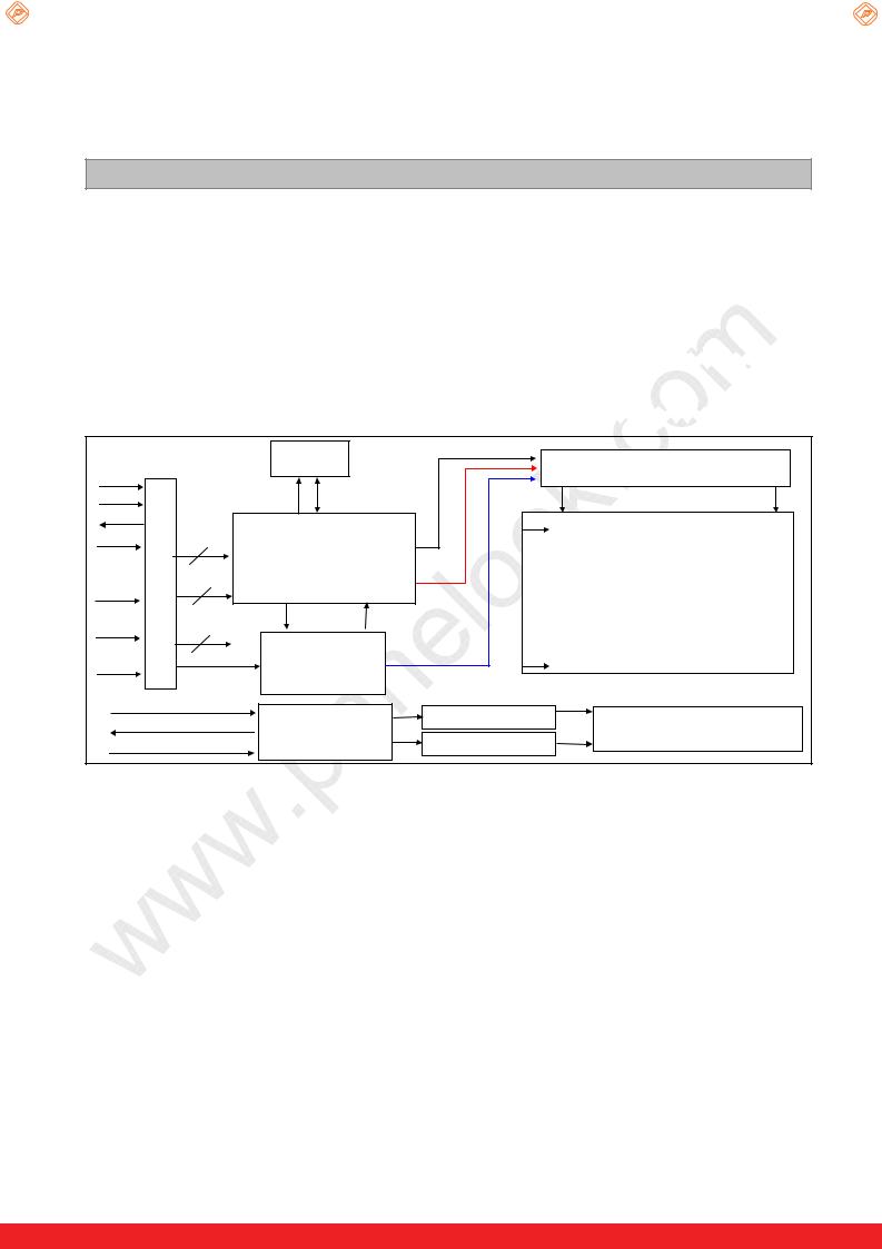
1. General Description
The LC420WUN is a Color Active Matrix Liquid Crystal Display with an integral External Electrode Fluorescent Lamp(EEFL) backlight system. The matrix employs a-Si Thin Film Transistor as the active element. It is a transmissive display type which is operating in the normally black mode. It has a 42.02 inch diagonally measured active display area with WUXGA resolution (1080 vertical by 1920 horizontal pixel array). Each pixel is divided into Red, Green and Blue sub-pixels or dots which are arrayed in vertical stripes. Gray scale or the luminance of the sub-pixel color is determined with a 10-bit gray scale signal for each dot. Therefore, it can present a palette of more than 1.06Bilion (true) colors. 


It has been designed to apply the 10-bit 2-port LVDS interface.
It is intended to support LCD TV, PCTV where high brightness, super wide viewing angle, high color gamut, high color depth and fast response time are important. 


|
|
EEPROM |
Mini-LVDS(RGB) |
|
||
|
|
|
|
Source Driver Circuit |
||
OPC Enable |
|
|
|
|
||
|
|
|
|
|
||
ExtVBR-B |
|
SCL |
SDA |
|
S1 |
S1920 |
VBR-B out |
|
|
|
G1 |
|
|
LVDS |
LVDS 1,2 |
Timing Controller |
|
|
TFT - LCD Panel |
|
2Port |
Option |
LVDS Rx + OPC + DGA + ODC |
|
|||
LVDS |
|
Integrated |
Control |
|
||
Select |
signal |
|
|
Signals |
|
(1920 Ý RGB Ý 1080 pixels) |
CN1 |
|
|
|
|||
|
|
|
|
|
[Gate In Panel] |
|
Bit |
(51pin) |
|
|
|
|
|
|
|
|
|
|
|
|
Select |
I2C |
|
|
|
|
|
+12.0V |
|
Power Circuit |
Power Signals |
G1080 |
|
|
|
|
Block |
|
|
|
|
|
|
|
|
|
|
|
|
EXTVBR-B |
|
|
3PinX1CN(High) |
|
|
|
Status |
|
Inverter |
Back light Assembly |
||
|
|
3PinX1CN(High) |
||||
|
+24.0V, GND |
|
|
|
||
|
|
|
|
|
|
|
General Features
Active Screen Size |
42.02 inches(1067.31mm) diagonal |
|
Outline Dimension |
983.0(H) x 576.0 (V) x 51.0 mm(D) (Typ.) |
|
Pixel Pitch |
0.4845 mm x 0.4845 mm |
|
Pixel Format |
1920 horiz. by 1080 vert. Pixels, RGB stripe arrangement |
|
Color Depth |
10bit(D) , 1.06Billon colors |
|
Luminance, White |
500 cd/m2 (Center 1point ,Typ.) |
|
Viewing Angle (CR>10) |
Viewing angle free ( R/L 178 (Min.), U/D 178 (Min.)) |
|
Power Consumption |
Total 156.8W (TYP.) (Logic=7.8W, Inverter=149W ) |
|
Weight |
9.1 Kg (Typ) |
|
Display Mode |
Transmissive mode, Normally black |
|
Surface Treatment |
Hard coating(3H), Anti-glare treatment of the front polarizer (Haze 10%) |
|
|
|
|
|
|
|
Ver. 1.0 |
4 /41 |
|
|
|
|
One step solution for LCD / PDP / OLED panel application: Datasheet, inventory and accessory! www.panelook.com
Global LCD Panel Exchange Center |
www.panelook.com |
LC420WUN
Product Specification
2. Absolute Maximum Ratings
The following items are maximum values which, if exceeded, may cause faulty operation or damage to the LCD module.
Table 1. ABSOLUTE MAXIMUM RATINGS
Parameter |
Symbol |
|
Value |
Unit |
Note |
||
|
|
|
|||||
Min |
|
Max |
|||||
|
|
|
|
|
|
||
Power Input Voltage |
LCD Circuit |
VLCD |
-0.3 |
|
+14.0 |
VDC |
|
Inverter |
VBL |
-0.3 |
|
+ 27.0 |
VDC |
|
|
|
|
|
|||||
Inverter Control Voltage |
ON/OFF |
VOFF / VON |
-0.3 |
|
+5.5 |
VDC |
1 |
Brightness |
VBR |
0.0 |
|
+5.0 |
VDC |
|
|
|
|
|
|||||
T-Con Option Selection Voltage |
VLOGIC |
-0.3 |
|
+4.0 |
VDC |
|
|
Operating Temperature |
TOP |
0 |
|
+50 |
¶C |
2,3 |
|
Storage Temperature |
TST |
-20 |
|
+60 |
¶C |
||
|
|
||||||
Panel Front Temperature |
TSUR |
- |
|
+68 |
¶C |
4 |
|
Operating Ambient Humidity |
HOP |
10 |
|
90 |
%RH |
2,3 |
|
Storage Humidity |
HST |
10 |
|
90 |
%RH |
||
|
|
||||||
|
|
|
|
|
|
|
|
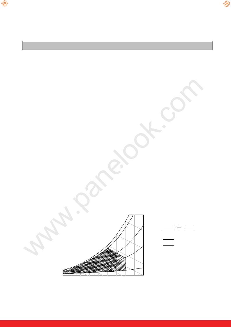
Note1. Ambient temperature condition (Ta = 25 2  ¶C )
¶C )

2.Temperature and relative humidity range are shown in the figure below. Wet bulb temperature should be Max 39¶C, and no condensation of water.
3.Gravity mura can be guaranteed below 40¶C condition.
4.The maximum operating temperatures is based on the test condition that the surface temperature
of display area is less than or equal to 68¶C with LCD module alone in a temperature controlled chamber. Thermal management should be considered in final product design to prevent the surface temperature of display area from being over 68 . The range of operating temperature may degraded in case of improper thermal management in final product design.
|
|
|
|
|
|
|
|
90% |
|
|
|
|
|
|
|
|
|
60 |
|
|
|
|
|
|
|
|
|
|
|
|
60% |
|
|
Wet Bulb |
|
|
|
50 |
|
|
[(%)RH] |
Storage |
|
|
|
|
|
|
|
|
|
|||
|
|
|
|
|
|
|
|
|
||
|
Temperature [¶C] |
|
40 |
|
|
|
|
|
||
|
|
|
|
|
|
|
|
Humidity |
|
|
|
|
|
|
|
|
|
|
|
40% |
Operation |
|
|
|
|
30 |
|
|
|
|
|
|
|
|
|
|
|
|
|
|
|
|
|
|
|
|
20 |
|
|
|
|
|
|
|
|
0 |
10 |
|
|
|
|
|
|
|
|
|
|
|
|
|
|
|
|
10% |
|
|
|
|
|
|
|
|
|
|
|
|
|
-20 |
0 |
10 |
20 |
30 |
40 |
50 |
60 |
70 |
80 |
|
|
|
Dry Bulb Temperature [¶C] |
|
|
|
|
||||
Ver. 1.0 |
5 /41 |
|
|
One step solution for LCD / PDP / OLED panel application: Datasheet, inventory and accessory! www.panelook.com
Global LCD Panel Exchange Center |
www.panelook.com |
LC420WUN
Product Specification
3. Electrical Specifications
3-1. Electrical Characteristics
It requires two power inputs. One is employed to power for the LCD circuit. The other Is used for the EEFL backlight and inverter circuit.
Table 2. ELECTRICAL CHARACTERISTICS
Parameter |
Symbol |
|
Value |
|
Unit |
Note |
|
Min |
Typ |
Max |
|||||
|
|
|
|
||||
Circuit : |
|
|
|
|
|
|
|
Power Input Voltage |
VLCD |
10.8 |
12.0 |
13.2 |
VDC |
|
|
Power Input Current (TBD) |
ILCD |
455 |
650 |
845 |
mA |
1 |
|
668 |
955 |
1240 |
mA |
2 |
|||
|
|
||||||
Power Consumption |
PLCD |
|
7.8 |
9.2 |
Watt |
1 |
|
Rush current |
IRUSH |
- |
- |
5.0 |
A |
3 |
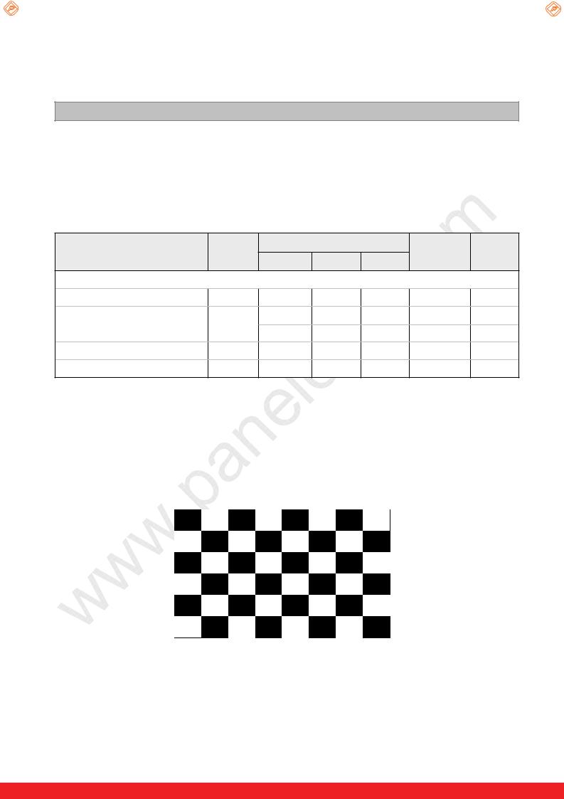
Note 1. The specified current and power consumption are under the VLCD=12.0V, Ta=25 2¶C, fV=60Hz condition whereas mosaic pattern(8 x 6) is displayed and fV is the frame frequency.
2.The current is specified at the maximum current pattern.
3.The duration of rush current is about 2ms and rising time of power input is 0.5ms (min.).
White : 1023 Gray
Black : 0 Gray
Mosaic Pattern(8 x 6) |
Ver. 1.0 |
6 /41 |
|
|
One step solution for LCD / PDP / OLED panel application: Datasheet, inventory and accessory! www.panelook.com

Global LCD Panel Exchange Center |
www.panelook.com |
|
|
|
|
|
|
|
|
|
LC420WUN |
|
|
|
|
|
Product Specification |
|
|
|
|
||
|
|
|
|
|
|
|
|
|
|
|
Table 3. ELECTRICAL CHARACTERISTICS (Continue) |
|
|
|
|
|
|||||
|
|
|
|
|
|
|
|
|
|
|
|
Parameter |
Symbol |
|
Values |
|
Unit |
Note |
|
||
|
|
|
|
|
||||||
|
Min |
Typ |
Max |
|
||||||
|
|
|
|
|
|
|
|
|||
|
|
|
|
|
|
|
|
|
|
|
Inverter : |
|
|
|
|
|
|
|
|
|
|
|
|
|
|
|
|
|
|
|
|
|
|
Power Supply Input Voltage |
VBL |
22.8 |
24.0 |
25.2 |
VDC |
1 |
|
||
|
Power Supply |
After Aging |
IBL_A |
- |
6.2 |
6.8 |
A |
1 |
|
|
|
Input Current |
Before Aging |
IBL_B |
- |
6.7 |
7.3 |
A |
2 |
|
|
|
|
|
||||||||
|
|
|
|
|
|
|
|
|
VBL = 22.8V |
|
|
Power Supply Input Current (In-Rush) |
IRUSH |
- |
- |
11 |
A |
EXTVBR-B = 100% |
|
||
|
|
|
|
|
|
|
|
|
6 |
|
|
Power Consumption (TBD) |
PBL |
- |
149 |
164 |
W |
1 |
|
||
|
|
On/Off |
On |
VON |
2.5 |
- |
5.0 |
VDC |
|
|
|
|
Off |
VOFF |
-0.3 |
0.0 |
0.8 |
VDC |
|
|
|
|
|
|
|
|
||||||
|
|
Brightness Adjust |
EXTVBR-B |
30 |
- |
100 |
% |
On Duty |
|
|
|
Input Voltage for |
7 |
|
|||||||
|
|
|
|
|
|
|
|
|
||
|
Control System |
PWM Frequency for |
PAL |
|
100 |
|
Hz |
5 |
|
|
|
Signals |
|
|
|
||||||
|
NTSC & PAL |
NTSC |
|
120 |
|
Hz |
5 |
|
||
|
|
|
|
|
||||||
|
|
Pulse Duty |
High Level |
2.5 |
- |
5.0 |
VDC |
High: Lamp on |
|
|
|
|
Level (PWM) |
|
|
|
|
|
|
||
|
|
Low Level |
0.0 |
- |
0.8 |
VDC |
Low : Lamp off |
|
||
|
|
(Burst mode) |
|
|||||||
|
|
|
|
|||||||
Lamp: |
|
|
|
|
|
|
|
|
|
|
Discharge Stabilization Time |
Ts |
|
|
3 |
min |
3 |
|
|||
|
Life Time |
|
|
|
50,000 |
60,000 |
|
Hrs |
4 |
|
|
|
|
|
|
|
|
|
|
|
|
Note 1. Electrical characteristics are determined after the unit has been ‘ON’ and stable for approximately 120 minutes at 25·2¶C. The specified current and power consumption are under the typical supply Input voltage 24Vand VBR (EXTVBR-B : 100%), it is total power consumption.
2.Electrical characteristics are determined within 30 minutes at 25·2¶C. The specified currents are under the typical supply Input voltage 24V.
3.The brightness of the lamp after lighted for 5minutes is defined as 100%.
TS is the time required for the brightness of the center of the lamp to be not less than 95% at typical current. The screen of LCD module may be partially dark by the time the brightness of lamp is stable after turn on.
4.Specified Values are for a single lamp which is aligned horizontally.
The life time is determined as the time which luminance of the lamp is 50% compared to that of initial value  at the typical lamp current (EXTVBR-B :100%), on condition of continuous operating at 25· 2¶C
5.LGD recommend that the PWM freq. is synchronized with Two times harmonic of Vsync signal of system.
6.The duration of rush current is about 10ms.
7.EXTVBR-B is based on input PWM duty of the inverter.
Ver. 1.0 |
7 /41 |
|
|
One step solution for LCD / PDP / OLED panel application: Datasheet, inventory and accessory! www.panelook.com

Global LCD Panel Exchange Center |
www.panelook.com |
LC420WUN
Product Specification
3-2. Interface Connections
This LCD module employs two kinds of interface connection, 51-pin connector is used for the module electronics and 14-pin connector is used for the integral backlight system.
3-2-1. LCD Module
- LCD Connector |
: FI-R51S-HF(manufactured by JAE) or KN25-51P-0.5SH(manufactured by Hirose) |
||||||
(CN1) |
Refer to below table |
|
|
|
|
||
- Mating Connector : FI-R51HL(JAE) or compatible |
|
|
|
|
|||
Table 4. MODULE CONNECTOR(CN1) PIN CONFIGURATION |
|
||||||
|
|
|
|
|
|
|
|
No |
|
Symbol |
Description |
|
No |
Symbol |
Description |
|
|
|
|
|
|
|
|
1 |
|
NC |
No Connection |
|
27 |
Bit Select |
‘H’ or NC= 10bit(D) , ‘L’ = 8bit |
2 |
|
NC |
No Connection |
|
28 |
R2AN |
SECOND LVDS Receiver Signal (A-) |
3 |
|
NC |
No Connection |
|
29 |
R2AP |
SECOND LVDS Receiver Signal (A+) |
4 |
|
NC |
No Connection (Reserved for LGD) |
|
30 |
R2BN |
SECOND LVDS Receiver Signal (B-) |
5 |
|
NC |
No Connection (Reserved for LGD) |
|
31 |
R2BP |
SECOND LVDS Receiver Signal (B+) |
6 |
|
NC |
No Connection (Reserved for LGD) |
|
32 |
R2CN |
SECOND LVDS Receiver Signal (C-) |
7 |
|
LVDS Select |
‘H’ =JEIDA , ‘L’ or NC = VESA |
|
33 |
R2CP |
SECOND LVDS Receiver Signal (C+) |
8 |
|
EXTVBR-B |
External VBR (From System) |
|
34 |
GND |
Ground |
9 |
|
VBR-B out |
OPC output (From LCM) |
|
35 |
R2CLKN |
SECOND LVDS Receiver Clock Signal(-) |
10 |
|
OPC Enable |
‘H’ = Enable , ‘L’ or NC = Disable |
|
36 |
R2CLKP |
SECOND LVDS Receiver Clock Signal(+) |
11 |
|
GND |
Ground |
|
37 |
GND |
Ground |
12 |
|
R1AN |
FIRST LVDS Receiver Signal (A-) |
|
38 |
R2DN |
SECOND LVDS Receiver Signal (D-) |
13 |
|
R1AP |
FIRST LVDS Receiver Signal (A+) |
|
39 |
R2DP |
SECOND LVDS Receiver Signal (D+) |
14 |
|
R1BN |
FIRST LVDS Receiver Signal (B-) |
|
40 |
R2EN |
SECOND LVDS Receiver Signal (E-) |
15 |
|
R1BP |
FIRST LVDS Receiver Signal (B+) |
|
41 |
R2EP |
SECOND LVDS Receiver Signal (E+) |
16 |
|
R1CN |
FIRST LVDS Receiver Signal (C-) |
|
42 |
NC |
No Connection |
17 |
|
R1CP |
FIRST LVDS Receiver Signal (C+) |
|
43 |
NC |
No Connection |
18 |
|
GND |
Ground |
|
44 |
GND |
Ground |
19 |
|
R1CLKN |
FIRST LVDS Receiver Clock Signal(-) |
|
45 |
GND |
Ground |
20 |
|
R1CLKP |
FIRST LVDS Receiver Clock Signal(+) |
|
46 |
GND |
Ground |
21 |
|
GND |
Ground |
|
47 |
NC |
No connection |
22 |
|
R1DN |
FIRST LVDS Receiver Signal (D-) |
|
48 |
VLCD |
Power Supply +12.0V |
23 |
|
R1DP |
FIRST LVDS Receiver Signal (D+) |
|
49 |
VLCD |
Power Supply +12.0V |
24 |
|
R1EN |
FIRST LVDS Receiver Signal (E-) |
|
50 |
VLCD |
Power Supply +12.0V |
25 |
|
R1EP |
FIRST LVDS Receiver Signal (E+) |
|
51 |
VLCD |
Power Supply +12.0V |
26 |
|
NC |
No Connection |
|
- |
- |
- |
Note |
1. All GND(ground) pins should be connected together to the LCD module’s metal frame. |
||||||
|
|
2. All VLCD (power input) pins should be connected together. |
|
||||
|
|
3. All Input levels of LVDS signals are based on the EIA 644 Standard. |
|||||
|
|
4. Specific pins(pin No. #2~#6) are used for internal data process of the LCD module. |
|||||
|
|
These pins should be no connection. |
|
|
|
|
|
5.Specific pins(pin No. # 8~#10) are used for OPC function of the LCD module.
If not used, these pins are no connection. (Please see the Appendix III-4 for more information.)
6.LVDS pin (pin No. #24,25,40,41) are used for 10Bit(D) of the LCD module. If used for 8Bit(R), these pins are no connection.
7.Specific pin No. #44 is used for “No signal detection” of system signal interface.
It should be GND for NSB(No Signal Black) during the system interface signal is not. If this pin is “H”, LCD Module displays AGP(Auto Generation Pattern).
Ver. 1.0 |
8 /41 |
|
|
One step solution for LCD / PDP / OLED panel application: Datasheet, inventory and accessory! www.panelook.com
Global LCD Panel Exchange Center |
www.panelook.com |
LC420WUN
Product Specification
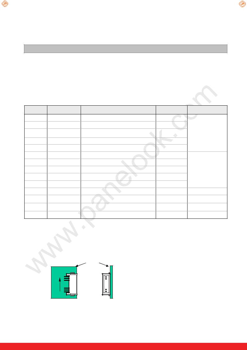
3-2-2. Backlight Module
[ Master ]
-Inverter Connector : 20022WR-14B1(Yeonho)
or Equivalent
- Mating Connector : 20022HS-14 or Equivalent
Table 5. INVERTER CONNECTOR PIN CONFIGULATION
Pin No |
Symbol |
Description |
Master |
Note |
1 |
VBL |
Power Supply +24.0V |
VBL |
|
2 |
VBL |
Power Supply +24.0V |
VBL |
|
3 |
VBL |
Power Supply +24.0V |
VBL |
|
4 |
VBL |
Power Supply +24.0V |
VBL |
|
5 |
VBL |
Power Supply +24.0V |
VBL |
|
6 |
GND |
Backlight Ground |
GND |
|
7 |
GND |
Backlight Ground |
GND |
|
8 |
GND |
Backlight Ground |
GND |
1 |
9 |
GND |
Backlight Ground |
GND |
|
10 |
GND |
Backlight Ground |
GND |
|
11 |
NC |
No Connection |
NC |
|
12 |
VON/OFF |
Backlight ON/OFF control |
VON/OFF |
3 |
13 |
EXTVBR-B |
External PWM |
EXTVBR-B |
3 |
14 |
Status |
Lamp Status |
Status |
2 |
Note 1. GND should be connected to the LCD module’s metal frame.
2.Normal : Low (under 0.7V) / Abnormal : High (upper 3.0V) Please see Appendix IV-1 for more information.
3.The impedance of pin #12 is over 50[K˟] & the impedance of Pin #13 is over 100[K˟].
• • Rear view of LCM |
|
PCB |
|
14 |
|
… |
… |
1 |
|
<Master> |
|
…
PCB 
1
…
12
<Slave>
Ver. 1.0 |
9 /41 |
|
|
One step solution for LCD / PDP / OLED panel application: Datasheet, inventory and accessory! www.panelook.com
Global LCD Panel Exchange Center |
www.panelook.com |
LC420WUN
Product Specification
3-3. Signal Timing Specifications
Table 6 shows the signal timing required at the input of the LVDS transmitter. All of the interface signal timings should be satisfied with the following specification for normal operation.
Table 6-1. TIMING TABLE for NTSC (DE Only Mode)
|
ITEM |
Symbol |
Min |
Typ |
Max |
Unit |
Note |
|
Display Period |
tHV |
- |
960 |
- |
tclk |
|
Horizontal |
Blank |
tHB |
100 |
140 |
240 |
tclk |
|
|
Total |
tHP |
1060 |
1100 |
1200 |
tclk |
2200/2 |
|
Display Period |
tVV |
- |
1080 |
- |
tHP |
|
Vertical |
Blank |
tVB |
11 |
45 |
69 |
tHP |
|
|
Total |
tVP |
1091 |
1125 |
1149 |
tHP |
|
|
DCLK |
fCLK |
70 |
74.25 |
77 |
MHz |
148.5/2 |
Frequency |
Horizontal |
fH |
65 |
67.5 |
70 |
KHz |
|
|
Vertical |
fV |
57 |
60 |
63 |
Hz |
|
Table 6-2. TIMING TABLE for PAL (DE Only Mode)
|
ITEM |
Symbol |
Min |
Typ |
Max |
Unit |
Note |
|
Display Period |
tHV |
- |
960 |
- |
tclk |
|
Horizontal |
Blank |
tHB |
100 |
140 |
240 |
tclk |
|
|
Total |
tHP |
1060 |
1100 |
1200 |
tclk |
2200/2 |
|
Display Period |
tVV |
- |
1080 |
- |
tHP |
|
Vertical |
Blank |
tVB |
228 |
270 |
300 |
tHP |
|
|
Total |
tVP |
1308 |
1350 |
1380 |
tHP |
|
|
DCLK |
fCLK |
70 |
74.25 |
77 |
MHz |
148.5/2 |
Frequency |
Horizontal |
fH |
65 |
67.5 |
70 |
KHz |
|
|
Vertical |
fV |
47 |
50 |
53 |
Hz |
|
Note The Input of HSYNC & VSYNC signal does not have an effect on normal operation(DE Only Mode). The performance of the electro-optical characteristics may be influenced by variance of the vertical refresh rate.
Ver. 1.0 |
10 /41 |
|
|
One step solution for LCD / PDP / OLED panel application: Datasheet, inventory and accessory! www.panelook.com
Global LCD Panel Exchange Center |
www.panelook.com |
LC420WUN
Product Specification
3-4. LVDS Signal Specification
3-4-1. LVDS Input Signal Timing Diagram
0.7VDD
DE, Data
0.3VDD
tCLK
0.5 VDD
DCLK
First data |
|
Invalid data |
|
|
|
Second data |
Invalid data |
||||
|
|
|
|
|
DE(Data Enable) |
|
|
|
|
|
|
|
|
|
|
|
|
|
|
|
|
|
|
|
Valid data |
|
|
Pixel |
0,0 |
Pixel |
2,0 |
|
Valid data |
|
|
Pixel |
1,0 |
Pixel |
3,0 |
Invalid data
Invalid data
tHV
tHP
1 |
1080 |
DE(Data Enable)
tVV
tVP
Ver. 1.0 |
11 /41 |
|
|
One step solution for LCD / PDP / OLED panel application: Datasheet, inventory and accessory! www.panelook.com
Global LCD Panel Exchange Center |
www.panelook.com |
LC420WUN
Product Specification
3-4-2. LVDS Input Signal Characteristics
1) DC Specification
LVDS |
- |
|
|
|
|
|
|
LVDS |
+ |
|
|
|
|
|
|
|
|
|
|
|
V CM |
V IN _ MAX |
V IN _ MIN |
|
# V CM = {( LVDS |
+) + ( LVDS - )} /2 |
|
|
|
|
|
0V |
|
|
|
|
|
|
|
Description |
Symbol |
Min |
Max |
Unit |
|
Note |
|
LVDS Common mode Voltage |
VCM |
1.0 |
1.5 |
V |
|
- |
|
LVDS Input Voltage Range |
VIN |
0.7 |
1.8 |
V |
|
- |
|
Change in common mode Voltage |
ȟVCM |
|
250 |
mV |
|
- |
|
2) AC Specification
|
|
|
|
Tclk |
LVDS Clock |
|
|
|
|
|
|
|
A |
|
LVDS Data |
|
|
|
|
|
|
tSKEW |
(Fclk |
= 1/Tclk ) |
|
|
tSKEW |
A |
|
|
|
|
|
|
|
|
|
Tclk |
|
LVDS 1’st Clock |
|
|
|
80% |
LVDS 2nd / 3rd / 4th |
Clock |
|
|
|
|
|
|
|
20% |
|
tSKEW_min |
tSKEW_max |
tRF |
|
|
|
|||
Description |
|
Symbol |
Min |
Max |
Unit |
Note |
|
LVDS Differential Voltage |
High Threshold |
|
VTH |
100 |
300 |
mV |
3 |
Low Threshold |
|
VTL |
-300 |
-100 |
mV |
||
|
|
|
|||||
LVDS Clock to Data Skew Margin |
|
tSKEW |
|
|(0.25*Tclk)/7| |
ps |
- |
|
LVDS Clock/DATA Rising/Falling time |
|
tRF |
260 |
(0.3*Tclk)/7 |
ps |
2 |
|
Effective time of LVDS |
|
teff |
·360 |
|
ps |
- |
|
LVDS Clock to Clock Skew Margin (Even to Odd) |
|
tSKEW_EO |
|
1/7* Tclk |
Tclk |
- |
|
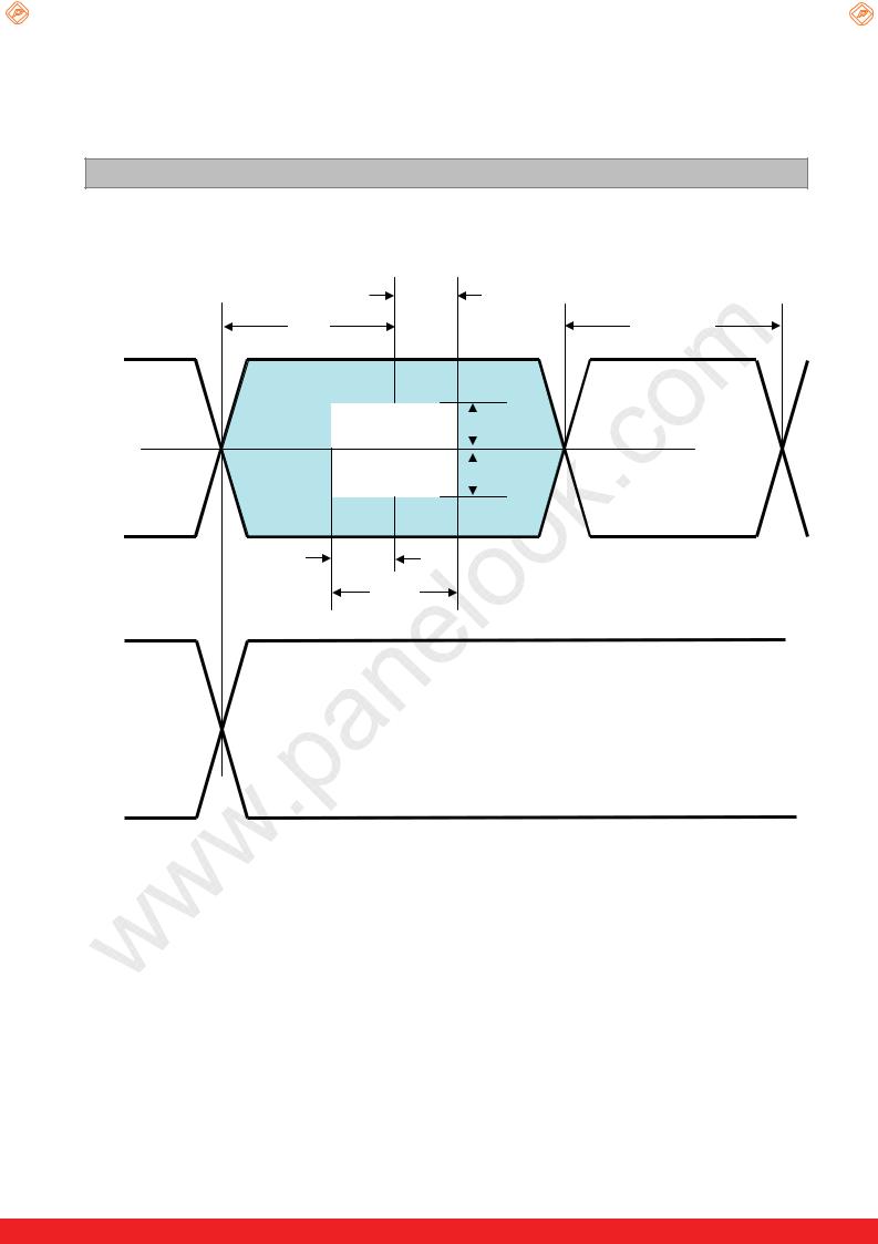
Note 1. All Input levels of LVDS signals are based on the EIA 644 Standard.
2.If tRF isn’t enough, teff should be meet the range.
3.LVDS Differential Voltage is defined within teff
Ver. 1.0 |
12 /41 |
|
|
One step solution for LCD / PDP / OLED panel application: Datasheet, inventory and accessory! www.panelook.com
Global LCD Panel Exchange Center |
www.panelook.com |
LC420WUN
Product Specification
|
360ps |
|
0.5tui |
tui |
|
V+ |
|
|
data |
|
|
|
VTH |
|
Vcm |
|
|
|
VTL |
|
V- |
360ps |
|
data |
||
|
||
|
teff |
|
V+ |
tui : Unit Interval |
|
clk |
|
|
Vcm |
|
|
V- |
|
|
clk |
|
Ver. 1.0 |
13 /41 |
|
|
One step solution for LCD / PDP / OLED panel application: Datasheet, inventory and accessory! www.panelook.com
 Loading...