


Global LCD Panel Exchange Center |
www.panelook.com |
LC320WXE
Product Specification
SPECIFICATION
FOR
APPROVAL
( |
) |
Preliminary Specification |
|
|
|
||
( |
) |
Final Specification |
|
|
|
||
|
|
|
|
|
|
|
|
|
|
Title |
|
32.0” WXGA TFT LCD |
|||
|
|
|
|
|
|
|
|
|
|
|
|
|
|
||
|
|
BUYER |
|
|
|
SUPPLIER |
LG Display Co., Ltd. |
|
|
|
|
|
|
|
|
|
|
|
|
|
|
*MODEL |
LC320WXE |
|
|
MODEL |
|
|
|
||
|
|
|
|
|
|
||
|
|
|
|
|
|
SUFFIX |
SBB1 |
|
|
|
|
|
|||
|
|
|
|
|
|
|
|
|
|
|
|
|
|
*When you obtain standard approval, |
|
please use the above model name without suffix
 SIGNATURE
APPROVED BY
DATE
/


 /
/ 
/
Please return 1 copy for your confirmation with your signature and comments.
APPROVED BY
SIGNATURE
DATE
S.S. Kim / Team Leader
REVIEWED BY
J.S. PARK / Sub Leader
PREPARED BY
Y.J. KIM / Engineer
TV Product Development Dept.
LG Display Co., Ltd
Ver. 0.5 |
1 / 27 |
|
|
One step solution for LCD / PDP / OLED panel application: Datasheet, inventory and accessory! www.panelook.com

Global LCD Panel Exchange Center |
www.panelook.com |
LC320WXE
Product Specification
|
CONTENTS |
|
Number |
ITEM |
Page |
|
COVER |
1 |
|
CONTENTS |
2 |
|
RECORD OF REVISIONS |
3 |
1 |
GENERAL DESCRIPTION |
4 |
2 |
ABSOLUTE MAXIMUM RATINGS |
5 |
3 |
ELECTRICAL SPECIFICATIONS |
6 |
3-1 |
ELECTRICAL CHARACTERISTICS |
6 |
3-2 |
INTERFACE CONNECTIONS |
8 |
3-3 |
SIGNAL TIMING SPECIFICATIONS |
10 |
3-4 |
SIGNAL TIMING WAVEFORMS |
12 |
3-5 |
COLOR DATA REFERENCE |
13 |
3-6 |
POWER SEQUENCE |
14 |
4 |
OPTICAL SPECIFICATIONS |
16 |
5 |
MECHANICAL CHARACTERISTICS |
20 |
6 |
RELIABILITY |
23 |
7 |
INTERNATIONAL STANDARDS |
24 |
7-1 |
SAFETY |
24 |
7-2 |
EMC |
24 |
8 |
PACKING |
25 |
8-1 |
DESIGNATION OF LOT MARK |
25 |
8-2 |
PACKING FORM |
25 |
9 |
PRECAUTIONS |
26 |
9-1 |
MOUNTING PRECAUTIONS |
26 |
9-2 |
OPERATING PRECAUTIONS |
26 |
9-3 |
ELECTROSTATIC DISCHARGE CONTROL |
27 |
9-4 |
PRECAUTIONS FOR STRONG LIGHT EXPOSURE |
27 |
9-5 |
STORAGE |
27 |
9-6 |
HANDLING PRECAUTIONS FOR PROTECTION FILM |
27 |
Ver. 0.5 |
|
2 / 27 |
One step solution for LCD / PDP / OLED panel application: Datasheet, inventory and accessory! www.panelook.com

Global LCD Panel Exchange Center |
www.panelook.com |
LC320WXE
Product Specification
RECORD OF REVISIONS
Revision No. |
Revision Date |
Page |
Description |
|
0.1 |
Jun, 30, 2008 |
- |
Preliminary Specification(First Draft) |
|
0.2 |
Jul, 14, 2008 |
21,22 |
Change of Mechanical drawing(Cover bottom) |
|
|
|
|
|
|
0.3 |
Aug, 12, 2008 |
1,A3-6,14 |
Change of Model Name(SBD1 SBB1) |
|
22 |
Change of Mechanical drawing(UDM Hole Size) |
|||
|
|
|||
0.4 |
Aug, 20, 2008 |
- |
Change of TBD SPEC |
|
|
|
4,20 |
Change of Weight |
|
0.5 |
Oct, 08, 2008 |
5,7-10 |
Change of Electrical Characteristics |
|
16,17 |
Change of Optical Spec |
|||
|
|
|||
|
|
A-9,12 |
|
|
|
|
|
|
|
|
|
|
|
|
|
|
|
|
|
|
|
|
|
|
|
|
|
|
|
|
|
|
|
|
|
|
|
|
|
|
|
|
|
|
|
|
|
|
|
|
|
|
|
|
|
|
|
|
|
|
|
|
|
|
|
|
|
|
|
|
|
|
|
|
|
|
|
|
|
|
|
|
|
|
|
|
|
|
|
|
|
|
|
|
|
|
|
|
|
|
|
|
|
|
|
|
|
|
|
|
|
|
|
|
|
|
|
|
Ver. 0.5 |
3 / 27 |
|
|
One step solution for LCD / PDP / OLED panel application: Datasheet, inventory and accessory! www.panelook.com
Global LCD Panel Exchange Center |
www.panelook.com |
LC320WXE
Product Specification
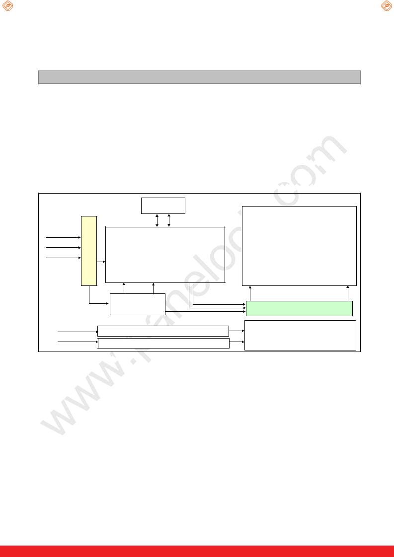
1. General Description
The LC320WXE is a Color Active Matrix Liquid Crystal Display with an integral External Electrode Fluorescent
Lamp(EEFL) backlight system. The matrix employs a-Si Thin Film Transistor as |
the active element. |
It is a transmissive type display operating in the normally black mode. It has a 31.51 inch |
diagonally measured |
active displa y area w ith W XGA resolut ion (768 vert ical b y 1366 hor izont al pixel array). Each pixel is divided into Red, Green and Blue sub-pixels or dots which are arranged in Horizontal stripes. Gray scale or the luminance of the sub-pixel color is determined with a 8-bit gray scale signal for each dot, thus presenting a palette of more than 16.7M(true) colors. 


It has been designed to apply the 8-bit 1-port LVDS interface.
It is intended to support LCD TV, PCTV where high brightness, super wide viewing angle, high color gamut, high color depth and fast response time are important. 


|
|
EEPROM |
|
|
||
|
|
SCL |
SDA |
|
|
|
+12.0V |
|
Timing Controller |
TFT - LCD Panel |
|||
LVDS 1Port |
CN1 |
|||||
[LVDS Rx + ODC + OPC |
|
(1366 768 x RGB pixels) |
||||
|
|
|||||
LVDS Select #9 |
(30pin) |
|
||||
|
+ SDRAM + Spread Spectrum |
|
[Gate In Panel] |
|||
|
|
|
||||
|
|
|
|
|||
|
|
integrated] |
|
|
||
|
|
Power Circuit |
RGB |
S1 |
S1366 |
|
|
|
|
|
|||
|
|
Block |
|
|
Source Driver Circuit |
|
High Input |
CN2, 3Pin, 12 Lamps/@93 mA |
|
|
|||
High Input |
Back light Assembly (12EEFL) |
|||||
CN3, 3Pin, 12 Lamps/@93 mA |
||||||
|
|
|
|
|||
General Features 

Active Screen Size |
31.51 inches(800.4mm) diagonal |
Outline Dimension |
760.0 mm(H) x 450.0 mm(V) x 43.0 mm(D) (Typ.) |
Pixel Pitch |
510.75 x 170.25 x RGB |
Pixel Format |
1366 horiz. by 768 vert. pixels RGB horizontal stripe arrangement |
Color Depth |
8bit, 16,7 M colors |
Luminance, White |
500 cd/m2 (Center 1 point) (Typ.) |
Viewing Angle (CR>10) |
Viewing angle free ( R/L 178(Min.), U/D 178(Min.)) |
Power Consumption |
Total 87.5Watt (Typ.) (Logic=3.5 W, Back Light= 84W @ with Inverter) |
Weight |
5,500g(Typ.) |
Display Operating Mode |
Transmissive mode, normally black |
Surface Treatment |
Hard coating(3H), anti-glare treatment of the front polarizer (Haze 10%) |
|
|
|
|
Ver. 0.5 |
4 / 27 |
|
|
One step solution for LCD / PDP / OLED panel application: Datasheet, inventory and accessory! www.panelook.com
Global LCD Panel Exchange Center |
www.panelook.com |
LC320WXE
Product Specification
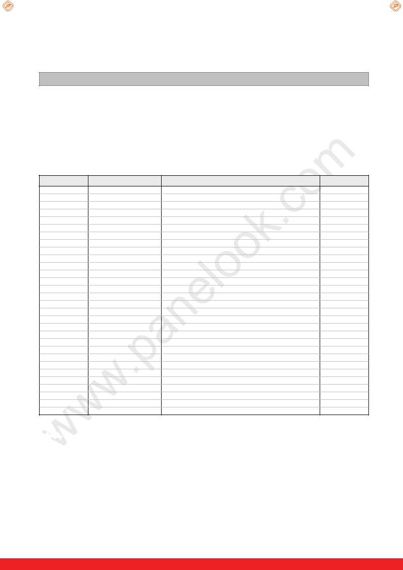
2. Absolute Maximum Ratings
The following items are maximum values which, if exceeded, may cause faulty operation or damage to the LCD module.
Table 1. ABSOLUTE MAXIMUM RATINGS
|
Parameter |
Symbol |
|
Value |
Unit |
Remark |
|
|
Min |
Max |
|||||
|
|
|
|
|
|||
Power Input |
VLCD |
-0.3 |
+14.0 |
VDC |
at 25 ± 2 C |
||
Voltage |
LCM |
||||||
|
|
|
|
|
|
||
B/L Input |
Operating Voltage |
VOP |
600 |
1300 |
V[ RMS] |
± |
|
voltage |
(one side) |
||||||
|
|
|
|
|
|||
Operating Temperature |
TOP |
0 |
+50 |
C |
|
||
Storage Temperature |
TST |
-20 |
+60 |
C |
Note 1,2 |
||
Operating Ambient Humidity |
HOP |
10 |
90 |
%RH |
|||
|
|||||||
Storage Humidity |
HST |
10 |
90 |
%RH |
|
||
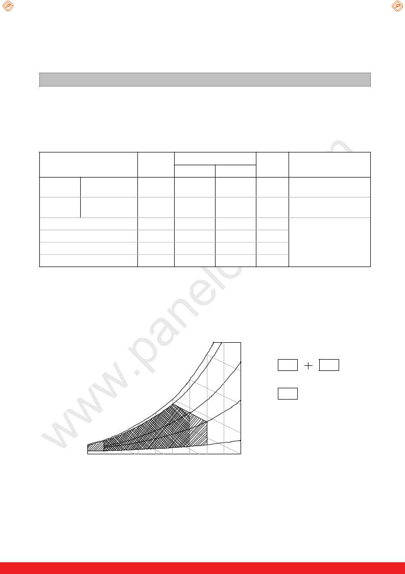
Notes : 1. Temperature and relative humidity range are shown in the figure below. Wet bulb temperature should be Max 39 C and no condensation of water.
2. Gravity mura can be guaranteed below 40 condition.
|
|
|
|
|
|
|
|
90% |
|
|
|
|
|
|
|
|
|
|
60 |
|
|
|
|
|
|
|
|
|
|
|
|
|
60% |
|
|
|
Wet Bulb |
|
|
40 |
50 |
|
|
|
[(%)RH] |
Storage |
|
|
|
|
|
|
|
|
|
||||
|
|
|
|
|
|
|
|
|
|
||
|
Temperature [ C] |
|
|
|
|
|
|
Humidity |
|
||
|
|
|
|
|
|
|
|
|
40% |
Operation |
|
|
|
|
|
|
|
|
|
|
|
||
|
|
|
|
30 |
|
|
|
|
|
|
|
|
|
|
|
|
|
|
|
|
|
|
|
|
|
|
20 |
|
|
|
|
|
|
|
|
|
|
10 |
|
|
|
|
|
|
|
|
|
|
0 |
|
|
|
|
|
|
|
10% |
|
|
|
|
|
|
|
|
|
|
|
|
|
|
-20 |
0 |
10 |
20 |
30 |
40 |
50 |
60 |
70 |
80 |
|
|
|
|
Dry Bulb Temperature [ C] |
|
|
|
|
|
||||
Ver. 0.5 |
5 / 27 |
|
|
One step solution for LCD / PDP / OLED panel application: Datasheet, inventory and accessory! www.panelook.com
Global LCD Panel Exchange Center |
www.panelook.com |
LC320WXE
Product Specification
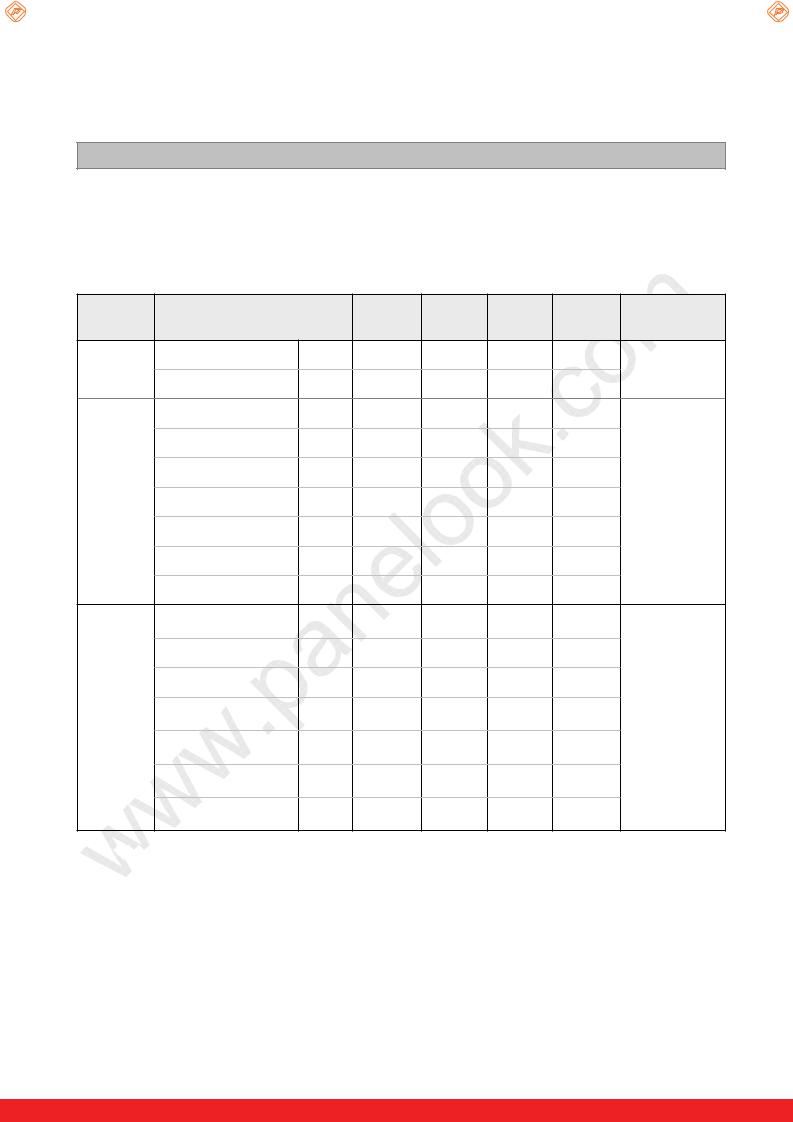
3. Electrical Specifications
3-1. Electrical Characteristics
It requires two power inputs. One is employed to power for the LCD circuit.
The other Is used for the EEFL backlight and inverter circuit.
Table 2. ELECTRICAL CHARACTERISTICS |
|
|
|
|
|
||
Parameter |
Symbol |
|
Value |
|
Unit |
Note |
|
|
|
|
|||||
|
|
Min |
Typ |
Max |
|
|
|
Circuit : |
|
|
|
|
|
|
|
Power Input Voltage |
VLCD |
10.8 |
12.0 |
13.2 |
VDC |
|
|
Power Input Current |
ILCD |
- |
290 |
380 |
mA |
1 |
|
- |
400 |
520 |
mA |
2 |
|||
|
|
||||||
Power Consumption |
PLCD |
- |
3.5 |
5.16 |
Watt |
1 |
|
Rush current |
IRUSH |
- |
- |
3.0 |
A |
3 |
|
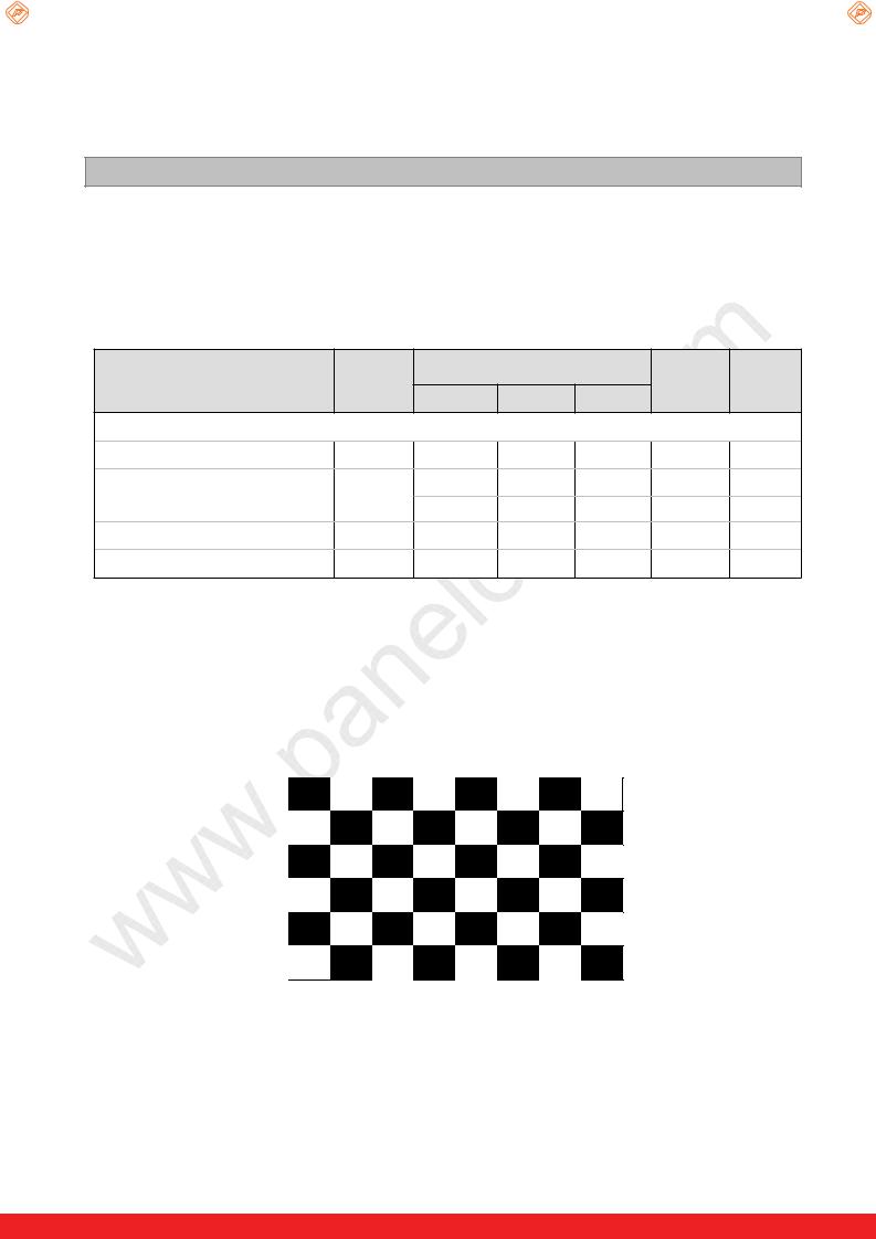
Notes : 1. The specified current and power consumption are under the VLCD=12.0V, 25 ± 2 C, fV=60Hz condition whereas mosaic pattern(8 x 6) is displayed and fV is the frame frequency.
2.The current is specified at maximum current pattern.
3.The duration of rush current is about 2ms and rising time of power input is 0.5ms (min.)
White : 255 Gray
Black : 0 Gray
Mosaic Pattern(8 x 6) |
Ver. 0.5 |
6 / 27 |
|
|
One step solution for LCD / PDP / OLED panel application: Datasheet, inventory and accessory! www.panelook.com

Global LCD Panel Exchange Center |
www.panelook.com |
|
|
|
|
|
|
|
|
|
|
|
LC320WXE |
|
|
|
|
|
|
|
|
|
|
|
|
|
|
|
Product Specification |
|
|
|
|
||||
|
Table 3. ELECTRICAL CHARACTERISTICS for IPB & Lamp |
|
|
|
|
||||||
|
Parameter |
|
Symbol |
|
|
|
Values |
|
|
Unit |
Notes |
|
|
|
|
|
|
|
|
||||
|
|
|
Min |
|
Typ |
Max |
|
||||
|
|
|
|
|
|
|
|
|
|||
|
Backlight Assembly : |
|
|
|
|
|
|
|
|
|
|
|
|
|
|
|
|
|
|
|
|
|
|
|
Operating Voltage |
|
VBL |
|
860 |
1020 |
1187 |
|
VRMS |
1, 2 |
|
|
(one side,fBL=63KHz, IBL= 93mArms)) |
|
|
||||||||
|
|
|
|
|
|
|
|
|
|
||
|
Operating Current (one side) |
|
IBL |
|
- |
93 |
- |
|
mARMS |
1 |
|
|
Established Starting |
0 |
VS |
|
- |
- |
1095 |
|
VRMS |
1, 3 |
|
|
Voltage (one side) |
25 |
|
- |
- |
920 |
|
||||
|
|
|
|
|
|
||||||
|
Operating Frequency |
|
fBL |
|
61 |
63 |
65 |
|
kHz |
4 |
|
|
Striking Time |
|
S TIME |
|
- |
- |
2 |
|
sec |
3 |
|
|
|
|
|
|
|
|
|
|
|
|
|
|
Power Consumption |
|
PBL |
|
|
84 |
|
|
Watt |
6 |
|
|
Burst Dimming Duty |
|
PWM duty |
|
20 |
|
|
100 |
|
% |
9 |
|
Burst Dimming Frequency |
|
1/T |
|
98 |
- |
182 |
|
Hz |
9 |
|
|
|
|
|
|
|
|
|
|
|
|
|
|
|
|
|
|
|
|
|
|
|
|
|
|
Parameter |
|
Symbol |
|
|
|
Values |
|
|
Unit |
Notes |
|
|
|
|
|
|
|
|
||||
|
|
|
Min |
|
Typ |
Max |
|
||||
|
|
|
|
|
|
|
|
|
|||
|
Lamp : APPENDIX-V |
|
|
|
|
|
|
|
|
|
|
|
|
|
|
|
|
|
|
|
|
|
|
|
Lamp Voltage (one side) |
|
VLAMP |
|
689 |
|
1035 |
1187 |
|
VRMS |
2 |
|
Lamp Current (one side) |
|
ILAMP |
|
3 |
|
7.75 |
8.5 |
|
mARMS |
|
|
Discharge Stabilization Time |
|
TS |
|
- |
|
- |
3 |
|
Min |
5 |
|
Lamp Frequency |
|
f LAMP |
|
40 |
|
63 |
80 |
|
KHz |
|
|
Lamp Temperature |
|
TLAMP |
|
|
|
|
130 |
|
C |
|
|
Established Starting |
0 |
VS |
|
|
|
|
1095 |
|
VRMS |
3 |
|
Voltage (one side) |
25 |
VS |
|
|
|
|
920 |
|
||
|
|
|
|
|
|
|
|
||||
|
Life Time |
|
|
|
50,000 |
|
|
|
|
Hrs |
7 |
Notes : The design of the inverter must have specifications for the lamp in LCD Assembly. |
|
|
|||||||||
|
The electrical characteristics of inverter are |
based on High-High Driving type. |
|
|
|||||||
The performance of the lamps in LCM, for example life time or brightness, is extremely influenced by the characteristics of the DC-AC inverter. So, all the parameters of an inverter should be carefully designed so as not to produce too much leakage current from high-voltage output of the inverter. When you design or order the inverter, please make sure unwanted lighting caused by the mismatch of the lamp and the inverter (no lighting, flicker, etc) has never been occurred. When you confirm it,
 the LCD– Assembly should be operated in the same condition as installed in your instrument.Do not attach a conductive tape to lamp connecting wire.
If you attach conductive tape to the lamp wire, not only luminance level can be lower than typical one
but also inverter operate abnormally on account of leakage current which is generated between lamp wire and conductive tape.
1.Specified values are defined for a Backlight Assembly.( IBL : 12 lamp, 7.75mA/Lamp)
2.Operating voltage is measured at 25 ± 2 C(after 2hr.aging). The variance range for operating voltage is ± 10%.
3.The established starting voltage [ VS ] should be applied to the lamps for more than Striking time (S TIME)
for start-up. Inverter open voltage must be more than established starting voltage. Otherwise, the lamps may not be turned on. The used lamp current is typical value.
Ver. 0.5 |
7 / 27 |
|
|
One step solution for LCD / PDP / OLED panel application: Datasheet, inventory and accessory! www.panelook.com
Global LCD Panel Exchange Center |
www.panelook.com |
LC320WXE
Product Specification
S TIME
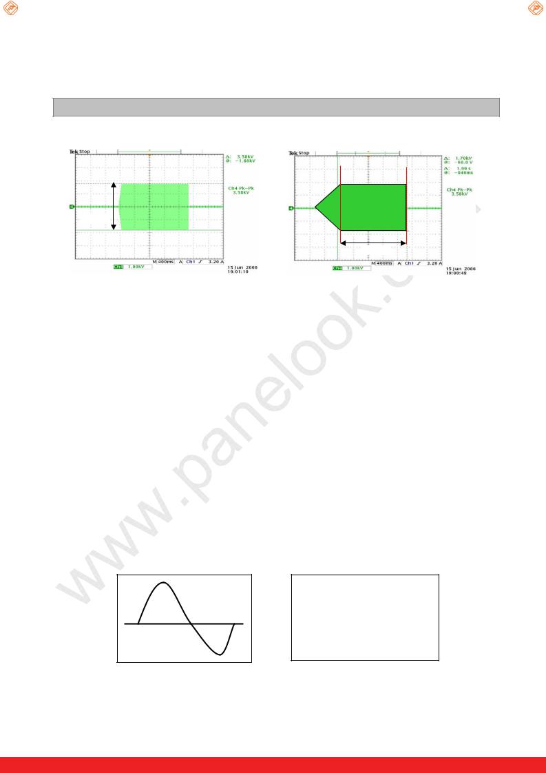
Vs = (Vpk-pk) / [ 2*root(2)]
4.Lamp frequency may produce interference with horizontal synchronous frequency. As a result, the may cause beat on the display. Therefore, lamp frequency shall be away as much as possible from the horizontal synchronous frequency and its harmonics range in order to prevent interference.
5.The brightness of the lamp after lighted for 5minutes is defined as 100%.
TS is the time required for the brightness of the center of the lamp to be not less than 95% at typical current. The screen of LCD module may be partially dark by the time the brightness of lamp is stable after turn on.
6.Maximum level of power consumption is measured at initial turn on.
Typical level of power consumption is measured after 2hrs aging at 25 ± 2 C.
7. The life time is determined as the time at which brightness of the lamp is 50% compared to that of initial value at the typical lamp current on condition of continuous operating at 25 ± 2 C, based on duty 100%.
8.The output of the inverter must have symmetrical(negative and positive) voltage and current waveform (Unsymmetrical ratio is less than 10%). Please do not use the inverter which has not only unsymmetrical voltage and current but also spike wave.
Requirements for a system inverter design, which is intended to achieve better display performance, power efficiency and more reliable lamp characteristics.
It can help increase the lamp lifetime and reduce leakage current.
a.The asymmetry rate of the inverter waveform should be less than 10%.
b.The distortion rate of the waveform should be within 2 10%.
* Inverter output waveform had better be more similar to ideal sine wave.
* Asymmetry rate:
I p
| I p – I –p | / Iop x 100%
* Distortion rate
I -p
I p (or I –p) / Iop
Ver. 0.5 |
8 / 27 |
|
|
One step solution for LCD / PDP / OLED panel application: Datasheet, inventory and accessory! www.panelook.com

Global LCD Panel Exchange Center |
www.panelook.com |
LC320WXE
Product Specification
9. The reference method of burst dimming duty ratio.
It is recommended to use synchronous V-sync frequency to prevent waterfall (Vsync x 2 =Burst Frequency)
|
|
|
|
|
|
|
|
|
|
||
|
|
|
|
|
|
PWM duty={ A/T } * 100 |
Point A |
|
Point B |
||
|
|
|
|
||
Point A |
: rising time 90% of Iout point . |
|
|
|
|
Point B |
: falling starting point . |
|
|
|
|
I out duty = { a/T } * 100 |
|
|
|
||
PWM Frequency = 1/T |
|
|
|
||
We recommend not to be much different between PWM duty and Iout duty .
Dimming current output rising and falling time may produce humming and inverter trans’ sound noise.
Burst dimming duty should be 100% for more than 1second after turn on.
Equipment 


Oscilloscope :TDS3054B(Tektronix)
Current Probe : P6022 AC (Tektronix)
High Voltage Probe: P5100(Tektronix)
10. The Cable between the backlight connector and its inverter power supply should be connected directly with a minimized length. The longer cable between the backlight and the inverter may cause the lower  luminance of lamp and may require more higher starting voltage ( Vs ).
11.The operating current must be measured as near as backlight assembly input.
12.The operating current unbalance between left and right must be under 10% of Typical currentLeft(Master) current – Right(Slave) Current 10% of typical current
Ver. 0.5 |
9 / 27 |
|
|
One step solution for LCD / PDP / OLED panel application: Datasheet, inventory and accessory! www.panelook.com
Global LCD Panel Exchange Center |
www.panelook.com |
LC320WXE
Product Specification
3-2. Interface Connections
This LCD module employs two kinds of interface connection, a 30-pin connector is used for the module electronics and 3-pin Balance PCB connector is used for the integral backlight system.
3-2-1. LCD Module
-LCD Connector(CN1) : FI-X30SSL-HF (Manufactured by JAE) or Equivalent -Mating Connector : FI-X30C2L (Manufactured by JAE) or Equivalent
Table 4. MODULE CONNECTOR(CN5) PIN CONFIGURATION |
|
||
Pin No. |
Symbol |
Description |
Note |
1 |
VLCD |
Power Supply +12.0V |
|
2 |
VLCD |
Power Supply +12.0V |
|
3 |
VLCD |
Power Supply +12.0V |
|
4 |
VLCD |
Power Supply +12.0V |
|
5 |
GND |
Ground |
|
6 |
GND |
Ground |
|
7 |
GND |
Ground |
|
8 |
GND |
Ground |
|
9 |
LVDS Select |
‘H’ =JEIDA , ‘L’ or NC = VESA |
Appendix VII |
10 |
|
No Connection |
|
11 |
GND |
Ground |
|
12 |
RA- |
LVDS Receiver Signal(-) |
|
13 |
RA+ |
LVDS Receiver Signal(+) |
|
14 |
GND |
Ground |
|
15 |
RB- |
LVDS Receiver Signal(-) |
|
16 |
RB+ |
LVDS Receiver Signal(+) |
|
17 |
GND |
Ground |
|
18 |
RC- |
LVDS Receiver Signal(-) |
|
19 |
RC+ |
LVDS Receiver Signal(+) |
|
20 |
GND |
Ground |
|
21 |
RCLK- |
LVDS Receiver Clock Signal(-) |
|
22 |
RCLK+ |
LVDS Receiver Clock Signal(+) |
|
23 |
GND |
Ground |
|
24 |
RD- |
LVDS Receiver Signal(-) |
|
25 |
RD+ |
LVDS Receiver Signal(+) |
|
26 |
GND |
Ground |
|
27 |
|
No Connection |
|
28 |
|
No Connection |
|
29 |
GND |
Ground |
|
30 |
GND |
Ground |
|
Notes : 1. All GND(ground) pins should be connected together to the LCD module’s metal frame.


 2. All VLCD (power input) pins should be connected together.
 3. All Input levels of LVDS signals are based on the EIA 644 Standard. (Please see the Appendix X)
4.Specific pin No. #30 is used for “No signal detection” of system signal interface.
It should be GND for NSB(No Signal Black) during the system interface signal is not. If this pin is “H”, LCD Module displays AGP(Auto Generation Pattern).
Ver. 0.5 |
10 / 27 |
|
|
One step solution for LCD / PDP / OLED panel application: Datasheet, inventory and accessory! www.panelook.com
Global LCD Panel Exchange Center |
www.panelook.com |
|
LC320WXE |
|
|
|
|
Product Specification |
|
|
3-2-2. Backlight Module |
|
|
[ Master ] |
[ Slave ] |
|
1) Balance Connector |
1) Balance Connector |
|
: 65002WS-03 (manufactured by YEONHO)or equivalent |
: 65002WS-03 (manufactured by YEONHO)or equivalent |
|
2) Mating Connector |
2) Mating Connector |
|
: 65002HS-03 (manufactured by YEONHO) or equivalent. : 65002HS-03 (manufactured by YEONHO) or equivalent.
Table 5. BACKLIGHT CONNECTOR PIN CONFIGURATION(CN2,CN3)
|
|
|
|
|
|
|
|
|
|
|
|
|
|
|
|
|
|
|
|
|
|
|
|
|
|
|
|
|
|
|
|
|
|
|
|
|
|
|
|
|
|
|
|
|
|
|
|
|
|
|
|||
|
|
|
|
|
|


|
|
Ver. 0.5 |
11 / 27 |
|
|
One step solution for LCD / PDP / OLED panel application: Datasheet, inventory and accessory! www.panelook.com
Global LCD Panel Exchange Center |
www.panelook.com |
LC320WXE
Product Specification
3-3. Signal Timing Specifications
Table 6-1 shows the signal timing required at the input of the LVDS transmitter. All of the interface signal timing should be satisfied with the following specification for normal operation.
[ DE (Data Enable) Only ]
ITEM |
Symbol |
|
Min |
Typ |
Max |
Unit |
Note |
|
|
Period |
tCLK |
12.5 |
13.8 |
15.8 |
ns |
|
|
DCLK |
|
|
|
|
|
|
|
|
|
Frequency |
- |
63 |
72.4 |
80 |
MHz |
|
|
|
Period |
tHT |
1456 |
1528 |
1920 |
tCLK |
|
|
|
Horizontal Valid |
tHV |
1366 |
1366 |
1366 |
tCLK |
|
|
|
Horizontal Blank |
- |
tHP- tHV |
162 |
tHP- tHV |
|
|
|
Hsync |
Frequency |
fH |
45 |
47.4 |
50 |
KHz |
|
|
|
Width |
tWH |
- |
32 |
- |
tCLK |
|
|
|
Horizontal Back Porch |
tHBP |
24 |
50 |
- |
|
|
|
|
Horizontal Front Porch |
tHFP |
40 |
80 |
- |
|
|
|
|
Period |
tVT |
776 |
790 |
1063 |
tHP |
|
|
|
(894) |
(948) |
(1008) |
|
||||
|
|
|
|
|
||||
|
Vertical Valid |
tVV |
768 |
768 |
768 |
tHP |
|
|
|
Vertical Blank |
- |
tVP- tVV |
22 |
tVP- tVV |
tHP |
|
|
|
Frequency |
fV |
57 |
60 |
63 |
Hz |
Note 1) |
|
Vsync |
NTSC : 57~63Hz |
|||||||
(47) |
(50) |
(53) |
||||||
|
|
|
||||||
|
|
|
|
(PAL : 47~53Hz) |
||||
|
Width |
tWV |
- |
5 |
- |
tHP |
||
|
|
|||||||
|
(12) |
|
||||||
|
|
|
|
|
|
|
||
|
Vertical Back Porch |
tVBP |
5 |
15 |
- |
Hz |
|
|
|
(128) |
|
||||||
|
|
|
|
|
|
|
||
|
Vertical Front Porch |
tVFP |
1 |
2 |
- |
tHP |
|
|
|
(40) |
|
||||||
|
|
|
|
|
|
|
Note :


 1. The input of HSYNC & VSYNC signal does not have an effect on normal operation(DE Only Mode). If you use spread spectrum of EMI, add some additional clock to minimum value for clock margin.
2.The performance of the electro-optical characteristics may be influenced by variance of the vertical refresh rate and the horizontal frequency
3.Timing should be set based on clock frequency.
Ver. 0.5 |
12 / 27 |
|
|
One step solution for LCD / PDP / OLED panel application: Datasheet, inventory and accessory! www.panelook.com
 Loading...