


Global LCD Panel Exchange Center |
www.panelook.com |
LM270WQ1
Liquid Crystal Display
Product Specification
SPECIFICATION
FOR
APPROVAL
( |
) Preliminary Specification |
|
|
|
|
||
( |
) Final Specification |
|
|
|
|
||
|
|
|
|
|
|
|
|
|
Title |
|
27.0” QHD TFT LCD |
|
|||
|
|
|
|
|
|
|
|
|
|
|
|
|
|
|
|
|
BUYER |
|
|
SUPPLIER |
|
LG Display Co., Ltd. |
|
|
|
|
|
|
|
|
|
|
|
|
|
|
*MODEL |
|
LM270WQ1 |
|
MODEL |
|
|
|
|
||
|
|
|
|
|
|
||
|
|
|
|
|
SUFFIX |
|
SLB1 |
|
|
|
|
||||
|
|
|
|
|
|
|
|


 *When you obtain standard approval,
please use the above model name without suffix
APPROVED BY
SIGNATURE


 DATE
DATE
/


 /
/
/
Please return 1 copy for your confirmation with your signature and comments.
APPROVED BY
SIGNATURE
DATE
S.Y. Park / G.Manager
REVIEWED BY
S. J. So / Manager
PREPARED BY
S. R. Yoo / Engineer
MNT Products Engineering Dept.
LG Display Co., Ltd.
Ver. 0.9 |
Mar. 15. 2012 |
1 / 33 |
|
|
|
One step solution for LCD / PDP / OLED panel application: Datasheet, inventory and accessory! www.panelook.com

Global LCD Panel Exchange Center |
www.panelook.com |
LM270WQ1
Liquid Crystal Display
Product Specification
|
|
Contents |
|
No |
|
ITEM |
Page |
|
COVER |
|
1 |
|
CONTENTS |
|
2 |
|
RECORD OF REVISIONS |
|
3 |
1 |
GENERAL DESCRIPTION |
|
4 |
2 |
ABSOLUTE MAXIMUM RATINGS |
|
5 |
3 |
ELECTRICAL SPECIFICATIONS |
|
6 |
3-1 |
ELECTRICAL CHARACTERISTICS |
|
6 |
3-2 |
INTERFACE CONNECTIONS |
|
8 |
3-3 |
LVDS CHARACTERISTICS |
|
11 |
3-4 |
SIGNAL TIMING SPECIFICATIONS |
|
14 |
3-5 |
SIGNAL TIMING WAVEFORMS |
|
15 |
3-6 COLOR INPUT DATA REFERNECE |
|
16 |
|
3-7 POWER SEQUENCE & DIP CONDITION FOR LCD MODULE |
17 |
||
3-8 POWER SEQUENCE & DIP CONDITION FOR LCD INVERTER |
19 |
||
4 |
OPTICAL SPECIFICATIONS |
|
20 |
5 |
MECHANICAL CHARACTERISTICS |
|
26 |
6 |
RELIABLITY |
|
29 |
7 |
INTERNATIONAL STANDARDS |
|
30 |
7-1 |
SAFETY |
|
30 |
7-2 |
EMC |
|
30 |
7-3 |
ENVIRONMENT |
|
30 |
8 |
PACKING |
|
31 |
8-1 DESIGNATION OF LOT MARK |
|
31 |
|
8-2 |
PACKING FORM |
|
31 |
9 |
PRECAUTIONS |
|
32 |
9-1 |
MOUNTING PRECAUTIONS |
|
32 |
9-2 |
OPERATING PRECAUTIONS |
|
32 |
9-3 |
ELECTROSTATIC DISCHARGE CONTROL |
|
33 |
9-4 |
PRECAUTIONS FOR STRONG LIGHT EXPOSURE |
33 |
|
9-5 |
STORAGE |
|
33 |
9-6 |
HANDLING PRECAUTIONS FOR PROTECTION FILM |
33 |
|
Ver. 0.9 |
Mar. 15. 2012 |
2 / 33 |
|
One step solution for LCD / PDP / OLED panel application: Datasheet, inventory and accessory! www.panelook.com

Global LCD Panel Exchange Center |
www.panelook.com |
LM270WQ1
Liquid Crystal Display
Product Specification
RECORD OF REVISIONS
Revision |
Revision |
Page |
|
Description |
No |
Date |
|
||
|
|
|
||
0.9 |
Mar. 15. 2012 |
- |
First Draft (Preliminary) |
|
Ver. 0.9 |
|
|
Mar. 15. 2012 |
3 / 33 |
One step solution for LCD / PDP / OLED panel application: Datasheet, inventory and accessory! www.panelook.com
Global LCD Panel Exchange Center |
www.panelook.com |
LM270WQ1
Liquid Crystal Display
Product Specification
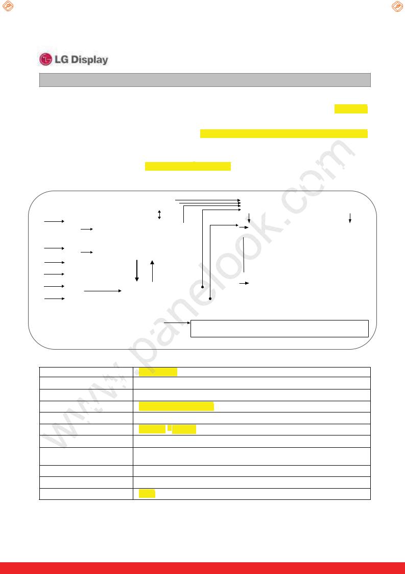
1. General Description
The LM270WQ1 is a Color Active Matrix Liquid Crystal Display with Light Emitting Diode ( White LED) backlight system without LED driver. The matrix employs a-Si Thin Film Transistor as the active element. It is a transmissive type display operating in the normally black mode. It has a 27inch diagonally measured
active display area with QHD resolution (2560 vertical by 1440 horizontal pixel array) Each pixel is divided into Red, Green and Blue sub-pixels or dots which are arranged in vertical stripes. Gray scale or the brightness of the sub-pixel color is determined with a 10-bit gray scale signal for each dot, thus, presenting a palette of more than 1.07Billion colors with Advanced-FRC (Frame Rate Control).

It has been designed to apply the 10-bit 4 port LVDS interface. 

 It is intended to support displays where high brightness, super wide viewing angle, high color saturation, and high color are important.


|
|
|
|
|
|
|
|
Mini-LVDS (RGB) |
|
|
|
||||
LVDS |
|
|
|
|
EEPROM |
|
|
|
Source Driver Circuit |
|
|||||
|
|
|
|
|
|
|
|
|
|
|
|
|
|||
|
|
|
|
|
|
|
|
|
|
|
|
|
|
||
|
|
|
|
|
|
|
|
|
|
|
|
|
|
|
|
|
|
|
|
I2C |
|
|
|
|
|
|
|
|
|||
2Port |
CN2 |
|
|
|
|
|
|
|
|
|
|
|
|||
|
|
|
|
|
|
|
S1 |
S2560 |
|
||||||
|
|
|
|
|
|
|
|
|
|
|
|
|
|||
|
(41pin) |
|
|
Timing |
|
|
|
|
|
G1 |
|
|
|||
LVDS |
|
|
|
|
|
|
|
|
|
|
|||||
|
|
|
|
|
|
|
|
|
|
|
|||||
2Port |
|
|
|
Controller |
|
|
|
|
|
TFT - LCD Panel |
|
||||
|
|
|
|
|
|
|
|
|
|||||||
|
|
|
|
|
|
|
|
|
|||||||
MSTAR |
|
|
|
|
|
|
|
|
|
|
|
|
|
||
Select |
|
|
|
|
|
|
|
|
|
|
|
|
(2560 Ý RGB Ý 1440 pixels) |
|
|
|
|
|
|
Logic Power |
|
|
|
|
|
|
|||||
Bit |
CN1 |
|
|
|
|
|
|
|
|
|
|||||
Select |
|
|
|
3.3V / 1.8V |
|
|
|
|
|
|
|
|
|||
(51pin) |
|
|
|
|
|
|
|
|
|
|
|
||||
ODC |
|
|
|
|
|
|
|
|
|
|
|
G1440 |
|
|
|
|
|
|
|
|
|
|
|
|
|
|
|
|
|
||
Select |
|
|
|
Power |
|
|
|
|
|
|
|
|
|
||
+12.0V |
|
|
|
|
|
|
|
|
|
|
|
|
|||
|
|
|
|
Circuit Block |
|
|
|
|
|
|
|
|
|
||
|
|
|
|
|
|
|
|
|
|
|
|
|
|||
|
|
|
|
|
|
|
|
|
|
|
|
|
|
|
|

 Vled
Vled
B/L System (White LED)
General Features
Active Screen Size 


Outline Dimension


Pixel Pitch
Pixel Format


Color Depth 

Luminance, White
Viewing Angle(CR>10)
Power Consumption
Weight
Display Operating Mode
Surface Treatment
26.96 inches (68.47cm) diagonal |
630.0(H) x 368.2(V) x 14.8(D) mm (Typ.) |
0.2331 mm x 0.2331 mm |
2560 horiz. By 1440 vert. Pixels RGB stripes arrangement |
1.07 Billion colors, 10Bit with A-FRC |
400cd/m 2 (1point)
View Angle Free (R/L 178(Typ.), U/D 178(Typ.))
Total 90.2Watt (Typ.)
(10.7Watt @VLCD, Max 79.5 Watt_Duty 100% of DC 350 mA_w/o driver) 3800 g (typ.)
Transmissive mode, normally black
Glare (Low Reflection treatment of the front polarizer)
Ver. 0.9 |
Mar. 15. 2012 |
4 / 33 |
|
|
|
One step solution for LCD / PDP / OLED panel application: Datasheet, inventory and accessory! www.panelook.com

Global LCD Panel Exchange Center |
www.panelook.com |
LM270WQ1
Liquid Crystal Display
Product Specification
2. Absolute Maximum Ratings
The following are maximum values which, if exceeded, may cause faulty operation or damage to the unit.
Table 1. ABSOLUTE MAXIMUM RATINGS
Parameter |
Symbol |
|
Values |
Units |
Notes |
|
Min |
Max |
|||||
|
|
|
|
|||
Power Input Voltage |
VLCD |
-0.3 |
14 |
Vdc |
at 25 2¶C |
|
Operating Temperature |
TOP |
0 |
50 |
¶C |
|
|
Storage Temperature |
TST |
-20 |
60 |
¶C |
1,2 |
|
Operating Ambient Humidity |
HOP |
10 |
90 |
%RH |
||
|
||||||
Storage Humidity |
HST |
10 |
90 |
%RH |
|
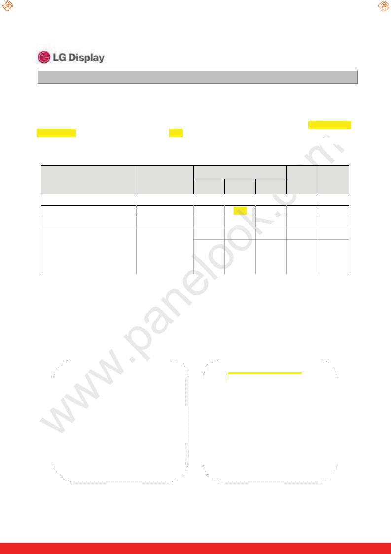
Note : 1. Temperature and relative humidity range are shown in the figure below. Wet bulb temperature should be 39 ¶C Max, and no condensation of water.
2. Storage condition is guaranteed under packing condition.
FIG.1 Temperature and relative humidity |
|
|
|
|
|
||||||
|
|
|
|
|
|
|
|
ڔڋڀ |
|
|
|
|
|
|
|
|
|
|
ڑڋ |
|
|
|
|
|
|
|
|
|
|
|
|
|
ڑڋڀ |
|
|
|
|
|
|
|
|
ڐڋ |
|
|
|
ڣېۈۄڿۄۏ۔ٻڶڃڀڄڭڣڸ |
ڮۏۊۍڼۂۀ |
|
ڲۀۏٻڝېۇڽ |
|
|
|
|
|
|
|
|
||
|
گۀۈۋۀۍڼۏېۍۀٻڶڞڸ |
|
|
|
|
|
|
|
|
||
|
|
|
|
|
ڏڋ |
|
|
|
|
|
|
|
|
|
|
|
|
|
|
|
ڏڋڀ |
|
ڪۋۀۍڼۏۄۊۉ |
|
|
|
|
ڎڋ |
|
|
|
|
|
|
|
|
|
|
|
|
|
|
|
|
|
|
|
|
|
|
ڍڋ |
|
|
|
|
|
|
|
|
|
|
ڌڋ |
|
|
|
|
|
|
|
|
|
|
ڋ |
|
|
|
|
|
|
|
ڌڋڀ |
|
|
|
|
|
|
|
|
|
|
|
|
|
|
ڈڍڋ |
ڋ |
ڌڋ |
ڍڋ |
ڎڋ |
ڏڋ |
ڐڋ |
ڑڋ |
ڒڋ |
ړڋ |
|
|
|
|
ڟۍ۔ٻڝېۇڽٻگۀۈۋۀۍڼۏېۍۀٻڶڞڸ |
|
|
|
|
|
||||
Ver. 0.9 |
Mar. 15. 2012 |
5 / 33 |
|
|
|
One step solution for LCD / PDP / OLED panel application: Datasheet, inventory and accessory! www.panelook.com
Global LCD Panel Exchange Center |
www.panelook.com |
LM270WQ1
Liquid Crystal Display
Product Specification
3. Electrical Specifications
3-1. Electrical Characteristics
It requires two power inputs. One is employed to power the LCD electronics and to drive the TFT array and liquid crystal. The second input power for the LED, is typically generated by LED driver. The LED driver is an external unit to the LCDs. 


Table 2-1. ELECTRICAL CHARACTERISTICS
Parameter |
Symbol |
|
Values |
|
Unit |
Notes |
|
Min |
Typ |
Max |
|||||
|
|
|
|
||||
MODULE : |
|
|
|
|
|
|
|
Power Supply Input voltage |
VLCD |
11.4 |
12.0 |
12.6 |
Vdc |
|
|
Permissive Power Input Ripple |
VdRF |
- |
|
400 |
mVp-p |
|
Power Supply Input Current |
ILCD |
- |
(890) |
(1020) |
mA |
1 |
|
- |
(1210) |
(1390) |
mA |
2 |
|||
|
|
||||||
|
|
|
|
|
|
|
|
Power Consumption |
PLCD |
- |
(10.7) |
(12.4) |
Watt |
1 |
|
|
|
|
|
|
|
|
|
Rush Current |
IRUSH_VLCD |
- |
- |
3.0 |
A |
3 |
|
|
|
|
|
|
|
|
Note :
1.The specified current and power consumption are under the VLCD=12.0V, 25 2¶C,fV=60Hz condition whereas mosaic pattern(8 x 6) is displayed and fV is the frame frequency.
2.The current is specified at the maximum current pattern.
3.The duration of rush current is about 2ms and rising time of power Input is 1ms(min.).
FIG.2 pattern for Electrical characteristics |
|
|
|
|||||||||
power consumption measurement |
|
power input ripple |
||||||||||
|
White : 255Gray |
|
|
|
||||||||
|
Black : 0Gray |
|
|
|
||||||||
|
Maximum current pattern |
|||||||||||
|
|
|
|
|
|
|
|
|
|
|
|
|
|
|
|
|
|
|
|
|
|
|
|
|
|
|
|
|
|
|
|
|
|
|
|
|
|
|
|
|
|
|
|
|
|
|
|
|
|
|
|
|
|
|
|
|
|
|
|
|
|
|
|
|
|
|
|
|
|
|
|
|
|
|
|
|
|
|
|
|
|
|
|
|
|
|
|
|
|
|
|
Mosaic Pattern(8 x 6) |
White Pattern |
|
|
|
Ver. 0.9 |
Mar. 15. 2012 |
6 / 33 |
|
|
|
One step solution for LCD / PDP / OLED panel application: Datasheet, inventory and accessory! www.panelook.com
Global LCD Panel Exchange Center |
www.panelook.com |
LM270WQ1
Liquid Crystal Display
Product Specification
Table 2-2. LED Bar ELECTRICAL CHARACTERISTICS
Parameter |
Symbol |
Condition |
|
Values |
|
Unit |
Notes |
|
|
|
|
||||||
Min. |
Typ. |
Max. |
||||||
|
|
|
|
|
||||
|
|
|
|
|
|
|
|
|
LED : |
|
|
|
|
|
|
1,7 |
|
|
|
|
|
|
|
|
|
|
LED String Current |
Is |
|
- |
350 |
365 |
mA |
2,7 |
|
|
|
|
|
|
|
|
|
|
LED String Voltage |
Vs |
|
43 |
48 |
53 |
V |
3,7 |
|
|
|
|
|
|
|
|
|
|
LED Bar Voltage |
VBar |
|
- |
216 |
229 |
V |
3,7 |
|
|
|
|
|
|
|
|
|
|
LED String Power |
Ps |
|
10.85 |
12.6 |
14.35 |
Watt |
4,6,7 |
|
|
|
|
|
|
|
|
|
|
LED Bar Power |
PBar |
|
- |
72 |
79.5 |
Watt |
4,6,7 |
|
|
|
|
|
|
|
|
|
|
LED Life Time |
LED_LT |
|
30,000 |
- |
- |
Hrs |
5,7 |
|
|
|
|
|
|
|
|
|
LED driver design guide
: The design of the LED driver must have specifications for the LED in LCD Assembly.
The performance of the LED in LCM, for example life time or brightness, is extremely influenced by the characteristics of the LED driver. 


So all the parameters of an LED driver should be carefully designed and output current should be Constant current control. 


When you design or order the LED driver, please make sure unwanted lighting caused by the mismatch of the LED and the LED driver (no lighting, flicker, etc) never occurs.
When you confirm it, the LCD module should be operated in the same condition as installed in your instrument.


1.Specified values are for a single LED bar including Left & Right Bar.
2.The specified current is input LED chip 100% duty current.
3.The specified voltage is input LED string and Bar voltage at typical 350 mA 100% duty current.
4.The specified power consumption is input LED string & bar power consumption at typical 350 mA 100% duty current. 
5.The life is determined as the time at which luminance of the LED is 50% compared to that of initial value at the typical LED current on condition of continuous operating at 25 2¶C.
6.The LED bar power consumption shown above does not include loss of external driver.
 The used LED bar current is the LED typical current. String Power Consumption is calculated with PS = VS x Is Bar Power Consumption is calculated with PL = VBarx Is
7. LED operating DC Forward Current and Junction Temperature must not exceed LED Max Ratings at 25 2¶C.
Ver. 0.9 |
Mar. 15. 2012 |
7 / 33 |
|
|
|
One step solution for LCD / PDP / OLED panel application: Datasheet, inventory and accessory! www.panelook.com
Global LCD Panel Exchange Center |
www.panelook.com |
LM270WQ1
Liquid Crystal Display
Product Specification
3-2. Interface Connections
This LCD module employs two kinds of interface connection, 51-pin and 41-pin connectors are used for the module electronics and 14-pin connectors are used for the integral backlight system.
3-2-1. LCD Module (CN1, CN2)
- LCD Connector(CN1): IS050-C51B-C39-A(manufactured by UJU) or FI-RE51S-HF(manufactured by JAE) or compatible. Refer to below and next Page table. 


 - Mating Connector : FI-RE51HL(JAE) or compatible


Table 3-1. MODULE CONNECTOR(CN1) PIN CONFIGURATION
No |
Symbol |
Description |
No |
Symbol |
Description |
1 |
GND |
Ground |
27 |
Bit Select |
‘H’ = 10bit , ‘L’ = 8bit |
2 |
NC |
No Connection |
28 |
R2AN |
SECOND LVDS Receiver Signal (A-) |
3 |
NC |
No Connection |
29 |
R2AP |
SECOND LVDS Receiver Signal (A+) |
4 |
NC |
No Connection |
30 |
R2BN |
SECOND LVDS Receiver Signal (B-) |
5 |
NC |
No Connection |
31 |
R2BP |
SECOND LVDS Receiver Signal (B+) |
6 |
ODC Select |
‘H’ or NC = Enable , ‘L’ = Disable |
32 |
R2CN |
SECOND LVDS Receiver Signal (C-) |
7 |
LVDS Format |
‘H’= MSTAR Concept , ‘L’=normal |
33 |
R2CP |
SECOND LVDS Receiver Signal (C+) |
8 |
NC |
No Connection |
34 |
GND |
Ground |
9 |
PWM_OUT |
Reference signal for inverter control |
35 |
R2CLKN |
SECOND LVDS Receiver Clock Signal(-) |
10 |
NC |
No Connection |
36 |
R2CLKP |
SECOND LVDS Receiver Clock Signal(+) |
11 |
GND |
Ground |
37 |
GND |
Ground |
12 |
R1AN |
FIRST LVDS Receiver Signal (A-) |
38 |
R2DN |
SECOND LVDS Receiver Signal (D-) |
13 |
R1AP |
FIRST LVDS Receiver Signal (A+) |
39 |
R2DP |
SECOND LVDS Receiver Signal (D+) |
14 |
R1BN |
FIRST LVDS Receiver Signal (B-) |
40 |
R2EN |
SECOND LVDS Receiver Signal (E-) |
15 |
R1BP |
FIRST LVDS Receiver Signal (B+) |
41 |
R2EP |
SECOND LVDS Receiver Signal (E+) |
16 |
R1CN |
FIRST LVDS Receiver Signal (C-) |
42 |
Reserved |
No connection or GND |
17 |
R1CP |
FIRST LVDS Receiver Signal (C+) |
43 |
Reserved |
No connection or GND |
18 |
GND |
Ground |
44 |
GND |
Ground |
19 |
R1CLKN |
FIRST LVDS Receiver Clock Signal(-) |
45 |
GND |
Ground |
20 |
R1CLKP |
FIRST LVDS Receiver Clock Signal(+) |
46 |
GND |
Ground |
21 |
GND |
Ground |
47 |
NC |
No connection |
22 |
R1DN |
FIRST LVDS Receiver Signal (D-) |
48 |
VLCD |
Power Supply +12.0V |
23 |
R1DP |
FIRST LVDS Receiver Signal (D+) |
49 |
VLCD |
Power Supply +12.0V |
24 |
R1EN |
FIRST LVDS Receiver Signal (E-) |
50 |
VLCD |
Power Supply +12.0V |
25 |
R1EP |
FIRST LVDS Receiver Signal (E+) |
51 |
VLCD |
Power Supply +12.0V |
26 |
Reserved |
No connection or GND |
- |
- |
- |
Notes : 1. All GND(ground) pins should be connected together to the LCD module’s metal frame.

 2. All VLCD (power input) pins should be connected together.

 3. All Input levels of LVDS signals are based on the EIA 644 Standard.
 4. Specific pins(pin No. #2~#6) are used for internal data process of the LCD module. If not used, these pins are no connection.
5.LVDS pin (pin No. #24,25,40,41) are used for 10Bit(D) of the LCD module. If used for 8Bit(R), these pins are no connection.
6.Specific pin No. #44 is used for “No signal detection” of system signal interface.
It should be GND for NSB(No Signal Black) during the system interface signal is not. If this pin is “H”, LCD Module displays AGP(Auto Generation Pattern).
Ver. 0.9 |
Mar. 15. 2012 |
8 / 33 |
|
|
|
One step solution for LCD / PDP / OLED panel application: Datasheet, inventory and accessory! www.panelook.com
Global LCD Panel Exchange Center |
www.panelook.com |
LM270WQ1
Liquid Crystal Display
Product Specification
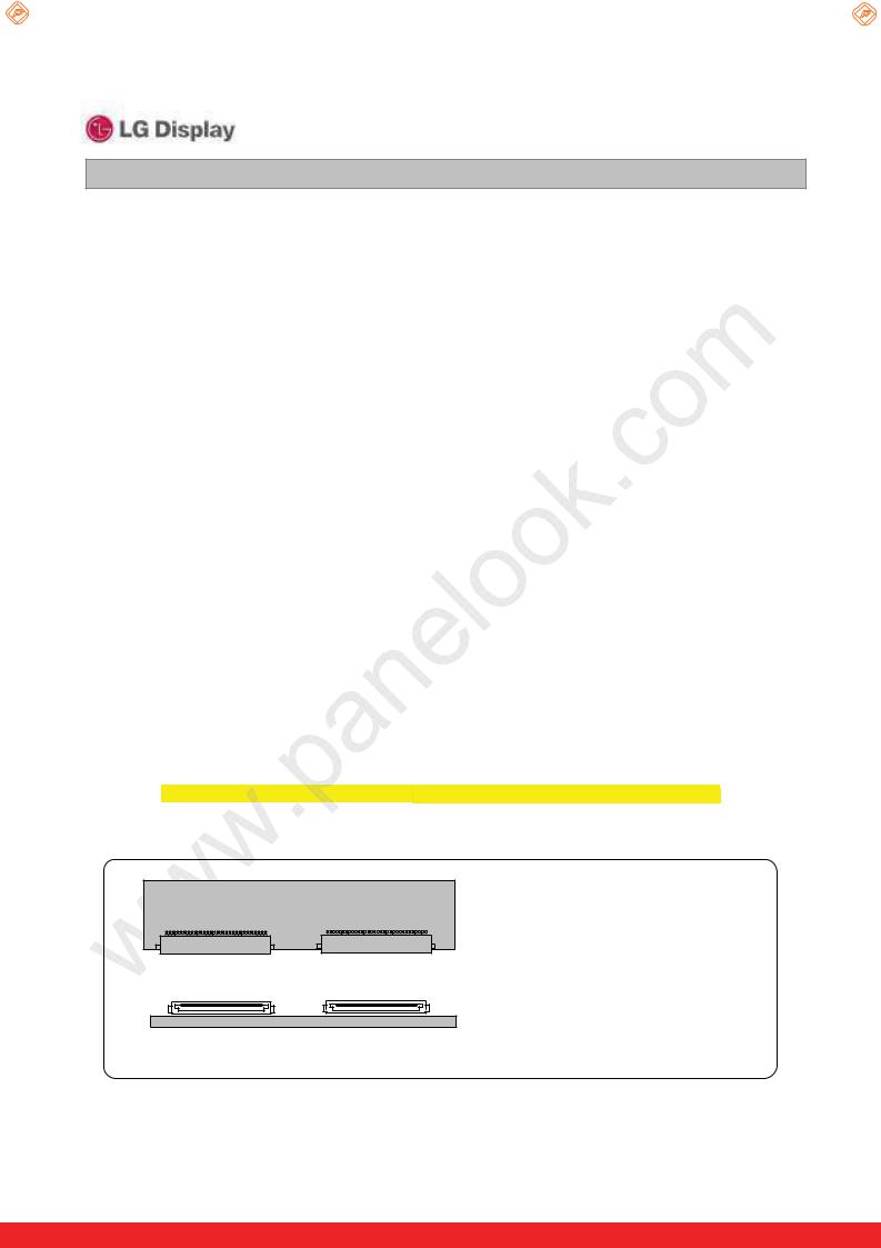
- LCD Connector(CN2): IS050-C41B-C39-A(manufactured by UJU) or FI-RE41S-HF(manufactured by JAE) or compatible. Refer to below table.
- Mating Connector : FI-RE41HL or compatible.
Table 3-2. MODULE CONNECTOR(CN2) PIN CONFIGURATION
No |
Symbol |
Description |
|
No |
Symbol |
Description |
1 |
NC |
No connection(Reserved) |
|
22 |
R3EN |
THIRD LVDS Receiver Signal (E-) |
2 |
NC |
No connection |
|
23 |
R3EP |
THIRD LVDS Receiver Signal (E+) |
3 |
NC |
No connection |
|
24 |
GND |
Ground |
4 |
NC |
No connection |
|
25 |
GND |
Ground |
5 |
NC |
No connection |
|
26 |
R4AN |
FORTH LVDS Receiver Signal (A-) |
6 |
NC |
No connection |
|
27 |
R4AP |
FORTH LVDS Receiver Signal (A+) |
7 |
NC |
No connection |
|
28 |
R4BN |
FORTH LVDS Receiver Signal (B-) |
8 |
NC |
No connection |
|
29 |
R4BP |
FORTH LVDS Receiver Signal (B+) |
9 |
GND |
Ground |
|
30 |
R4CN |
FORTH LVDS Receiver Signal (C-) |
10 |
R3AN |
THIRD LVDS Receiver Signal (A-) |
|
31 |
R4CP |
FORTH LVDS Receiver Signal (C+) |
11 |
R3AP |
THIRD LVDS Receiver Signal (A+) |
|
32 |
GND |
Ground |
12 |
R3BN |
THIRD LVDS Receiver Signal (B-) |
|
33 |
R4CLKN |
FORTH LVDS Receiver Clock Signal(-) |
13 |
R3BP |
THIRD LVDS Receiver Signal (B+) |
|
34 |
R4CLKP |
FORTH LVDS Receiver Clock Signal(+) |
14 |
R3CN |
THIRD LVDS Receiver Signal (C-) |
|
35 |
GND |
Ground |
15 |
R3CP |
THIRD LVDS Receiver Signal (C+) |
|
36 |
R4DN |
FORTH LVDS Receiver Signal (D-) |
16 |
GND |
Ground |
|
37 |
R4DP |
FORTH LVDS Receiver Signal (D+) |
17 |
R3CLKN |
THIRD LVDS Receiver Clock Signal(-) |
|
38 |
R4EN |
FORTH LVDS Receiver Signal (E-) |
18 |
R3CLKP |
THIRD LVDS Receiver Clock Signal(+) |
|
39 |
R4EP |
FORTH LVDS Receiver Signal (E+) |
19 |
GND |
Ground |
|
40 |
GND |
Ground |
20 |
R3DN |
THIRD LVDS Receiver Signal (D-) |
|
41 |
GND |
Ground |
21 |
R3DP |
THIRD LVDS Receiver Signal (D+) |
|
- |
|
|
Notes : 1. All GND(ground) pins should be connected together to the LCD module’s metal frame.
2.LVDS pin (pin No. #22,23,38,39) are used for 10Bit(D) of the LCD module. If used for 8Bit(R), these pins are no connection.
#1 |
CN1 |
#51 |
#1 |
CN2 |
#41 |
|
|
||||
#1 |
|
#51 |
#1 |
|
#41 |
Rear view of LCM
[CN1]
-Part/No. : IS050-C51B-C39-A(UJU)
-Mating connector : FI-RE51HL (Manufactured by JAE)
[CN2]
-Part/No. : IS050-C41B-C39-A(UJU)
-Mating connector : FI-RE41HL (Manufactured by JAE)
Ver. 0.9 |
Mar. 15. 2012 |
9 / 33 |
|
|
|
One step solution for LCD / PDP / OLED panel application: Datasheet, inventory and accessory! www.panelook.com
Global LCD Panel Exchange Center |
www.panelook.com |
LM270WQ1
Liquid Crystal Display
Product Specification
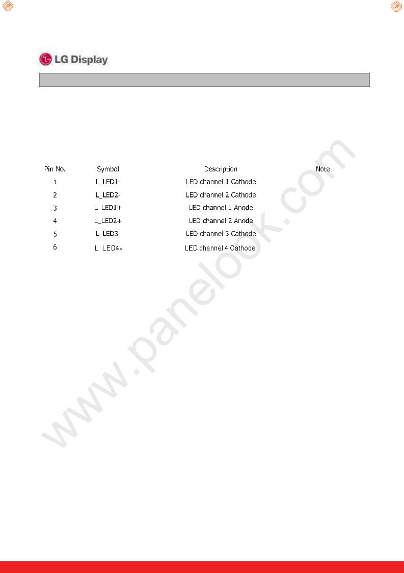
3-2-2. Backlight Interface
-LED Connector : H401K-D12N-12B (Manufactured by E&T)
-Mating Connector : 4530K-F12N-01R (Manufactured by E&T)
Table 5. LED CONNECTOR PIN CONFIGULATION
|
|
|
|
|
|
|
|
|
|
|
|
|
|
|
|
|
|
|
|
|
|
|
|
|
|
|
|
|
|
|
|
|
|
|
|
|
|
|
|
|
|
|
|
|
|
|
|
|
|
|
|
|
|
|
|
|
|
|
|
|
|
|
|
|
|
|
|
|
|
|
|
|
Ver. 0.9 |
Mar. 15. 2012 |
10 / 33 |
||||
|
|
|
|
|
|
|
|
One step solution for LCD / PDP / OLED panel application: Datasheet, inventory and accessory! www.panelook.com
 Loading...