


Global LCD Panel Exchange Center |
www.panelook.com |
LC320EXJ
Product Specification
SPECIFICATION
FOR
APPROVAL
( |
) |
Preliminary Specification |
( |
) |
Final Specification |
Title |
|
|
|
32.0” WXGA TFT LCD |
|
|
|||
|
|
|
|
|
|
|
|
|
|
|
|
|
|
|
|
|
|
|
|
BUYER |
|
Quatius |
|
|
|
SUPPLIER |
LG Display Co., Ltd. |
|
|
|
|
|
|
|
|
*MODEL |
LC320EXJ |
|
|
MODEL |
|
|
|
|
|
|
|
||
|
|
|
|
|
|
|
|
|
|
|
|
|
|
|
|
SUFFIX |
SEE1 (RoHS Verified) |
|
|
|
|
|
|
|
|||||
|
|
|
|
|
|
|
|
|
|
|
|
|
|
|
|
*When you obtain standard approval, |
|
|
|
|
|
|
|
|
|
please use the above model name without suffix |
|
|
|
|
|
|
|
|
|
|
|
|
|
APPROVED BY
SIGNATURE


 DATE
DATE
/


 /
/
/
Please return 1 copy for your confirmation with your signature and comments.
APPROVED BY |
SIGNATURE |
|
DATE |
||
|
J.T. Kim / Team Leader
REVIEWED BY
S.Y. Lee / Project Leader
PREPARED BY
Q-H. Jo / Engineer
TV Product Development Dept.
LG Display Co., Ltd.
Ver. 1.0 |
1 /34 |
|
|
One step solution for LCD / PDP / OLED panel application: Datasheet, inventory and accessory! www.panelook.com

Global LCD Panel Exchange Center |
www.panelook.com |
LC320EXJ
Product Specification
|
CONTENTS |
|
Number |
ITEM |
Page |
|
COVER |
1 |
|
CONTENTS |
2 |
|
RECORD OF REVISIONS |
3 |
1 |
GENERAL DESCRIPTION |
4 |
2 |
ABSOLUTE MAXIMUM RATINGS |
5 |
3 |
ELECTRICAL SPECIFICATIONS |
6 |
3-1 |
ELECTRICAL CHARACTERISTICS |
6 |
3-2 |
INTERFACE CONNECTIONS |
7 |
3-3 |
SIGNAL TIMING SPECIFICATIONS |
8 |
3-4 |
SIGNAL TIMING WAVEFORMS |
9 |
3-5 |
COLOR DATA REFERENCE |
12 |
3-6 |
POWER SEQUENCE |
13 |
4 |
OPTICAL SPECIFICATIONS |
14 |
5 |
MECHANICAL CHARACTERISTICS |
17 |
6 |
MECHANICAL DIMENSION |
18 |
6-1 |
BOARD ASSEMBLY DIMENSION |
18 |
6-2 |
CONTROL BOARD ASSEMBLY DIMENSION |
19 |
7 |
RELIABILITY |
20 |
8 |
INTERNATIONAL STANDARDS |
21 |
8-1 |
ENVIRONMENT |
21 |
9 |
PACKING |
22 |
9-1 |
PACKING FORM |
22 |
10 |
PRECAUTIONS |
23 |
10-1 |
ASSEMBLY PRECAUTIONS |
23 |
10-2 |
OPERATING PRECAUTIONS |
23 |
10-3 |
ELECTROSTATIC DISCHARGE CONTROL |
24 |
10-4 |
PRECAUTIONS FOR STRONG LIGHT EXPOSURE |
24 |
10-5 |
STORAGE |
24 |
10-6 |
OPERATING CONDITION GUIDE |
24 |
Ver. 1.0 |
|
2 /34 |
One step solution for LCD / PDP / OLED panel application: Datasheet, inventory and accessory! www.panelook.com

Global LCD Panel Exchange Center |
www.panelook.com |
LC320EXJ
Product Specification
RECORD OF REVISIONS
Revision No. |
Revision Date |
Page |
Description |
0.0 |
Apr. 30, 2012 |
- |
Preliminary Specification (First Draft) |
Ver. 1.0 |
|
|
3 /34 |
One step solution for LCD / PDP / OLED panel application: Datasheet, inventory and accessory! www.panelook.com
Global LCD Panel Exchange Center |
www.panelook.com |
LC320EXJ
Product Specification
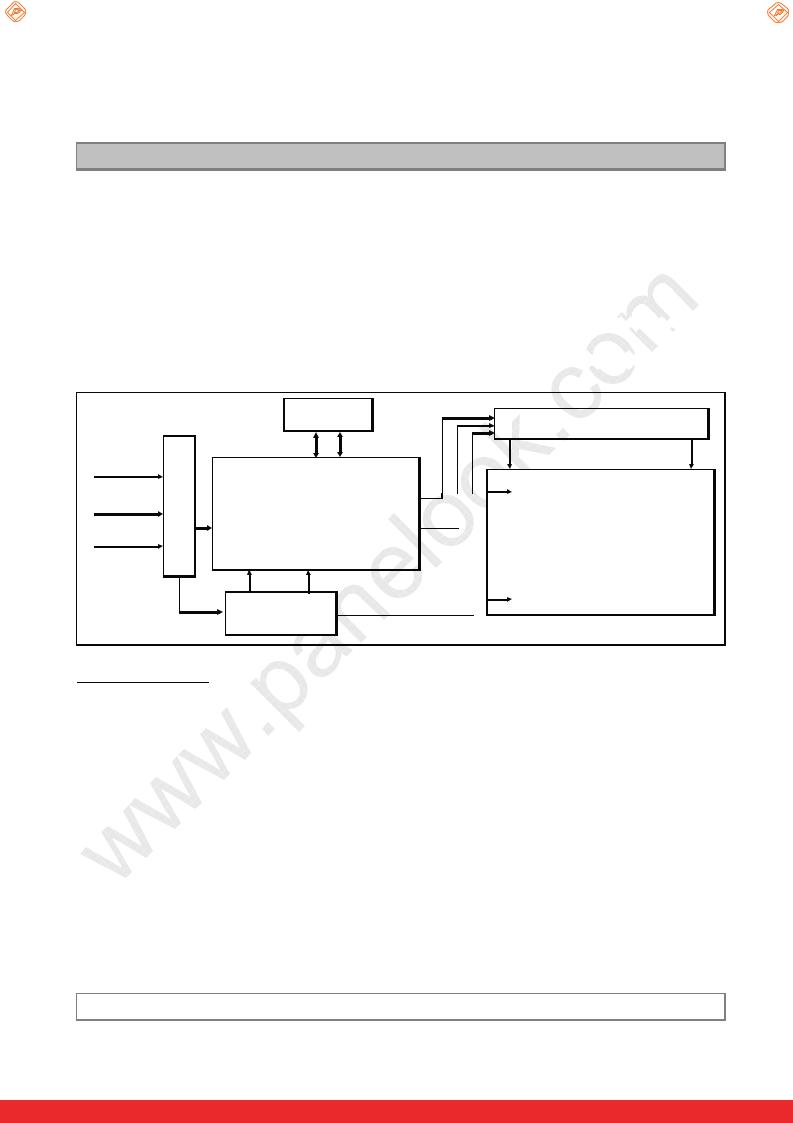
1. General Description
The LC320EXJ is a Color Active Matrix Liquid Crystal Display with an integral the Source PCB and Gate
implanted on Panel (GIP). The matrix employs a-Si Thin Film Transistor as |
the active element. |
It is a transmissive type display operating in the normally black mode. It has a 31.5 inch |
diagonally measured |
active display area with WXGA resolution (768 vertical by 1366 horizontal pixel array). Each pixel is divided into Red, Green and Blue sub-pixels or dots which are arranged in vertical stripes. Gray scale or the luminance of the sub-pixel color is determined with a 8-bit gray scale signal for each dot. Therefore, it can present a palette of more than 16.7M(6bit + A-FRC) colors. 


It is intended to support LCD TV, PCTV where high brightness, super wide viewing angle, high color gamut, high color depth and fast response time are important. 


|
|
EEPROM |
RGB |
|
|
|
|
Source Driver Circuit |
|
||
|
|
|
|
|
|
|
|
SCL |
SDA |
S1366 |
|
|
|
|
|
S1 |
|
LVDS Select #9 |
|
|
|
G1 |
|
|
|
|
|
|
|
LVDS 1Port |
CN1 |
Timing Controller |
|
|
|
(30pin) |
|
|
|
||
|
|
[LVDS Rx] |
|
Control |
|
+12.0V |
|
|
|
Signals |
|
|
|
|
|
|
|
|
|
|
|
G768 |
|
|
|
Power Circuit |
|
|
|
|
|
Block |
|
Power Signals |
|
General Features
Active Screen Size |
31.5 inches(800.4mm) diagonal |
||
Outline Dimension |
715.0mm(H) x 411.0mm(V) x 1.4mm(D) (Typ.) |
||
Pixel Pitch |
0.51075 |
X 0.51075 |
|
|
|
|
|
Pixel Format |
1366 horiz. by 768 vert. pixels RGB stripe arrangement |
||
Color Depth |
8bit(D), |
16,7 M colors |
|
Drive IC Data Interface |
Source D-IC : 6-bit mini-LVDS, gamma reference voltage, and control signals |
||
Gate D-IC : Gate In Panel |
|||
|
|||
Transmittance (With POL) |
5.62 %(Typ.) |
||
Viewing Angle (CR>10) |
Viewing angle free ( R/L 178 (Min.), U/D 178 (Min.)) |
||
Weight |
1.10Kg (Typ.) |
||
Display Mode |
Transmissive mode, Normally black |
||
Surface Treatment (Top) |
Hard coating(3H), Anti-glare treatment (Haze 1%) |
||
|
|
|
|
Ver. 1.0 |
4 /34 |
|
|
One step solution for LCD / PDP / OLED panel application: Datasheet, inventory and accessory! www.panelook.com
Global LCD Panel Exchange Center |
www.panelook.com |
LC320EXJ
Product Specification
2. Absolute Maximum Ratings
The following items are maximum values which, if exceeded, may cause faulty operation or damage to the LCD module.
Table 1. ABSOLUTE MAXIMUM RATINGS
Parameter |
Symbol |
|
Value |
Unit |
Remark |
|
Min |
Max |
|||||
|
|
|
|
|||
Power Input voltage |
VLCD |
-0.3 |
+14.0 |
V [DC] |
X |
|
Panel Front Temperature |
TSUR |
- |
+68 |
¶C |
4 |
|
Operating Temperature |
TOP |
0 |
+50 |
¶C |
|
|
Storage Temperature |
TST |
-20 |
+60 |
¶C |
2,3 |
|
Operating Ambient Humidity |
HOP |
10 |
90 |
%RH |
||
|
||||||
Storage Humidity |
HST |
10 |
90 |
%RH |
|
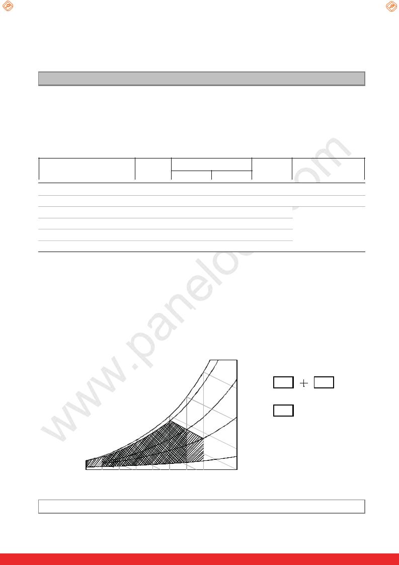
Note: 1. |
Ambient temperature condition (Ta = 25 2 ¶C ) |
2. |
Temperature and relative humidity range are shown in the figure below. Wet bulb temperature |
|
should be Max 39 ¶C and no condensation of water. |
3. |
Gravity mura can be guaranteed below 40 condition. |
4. |
The maximum operating temperature is based on the test condition that the surface temperature |
of display area is less than or equal to 68 with LCD module alone in a temperature controlled chamber. Thermal management should be considered in final product design to prevent the surface temperature of display area
 from being over 68 . The range of operating temperature may degrade in case of improper thermal management in final product design.
|
|
|
|
|
|
|
|
|
|
90% |
|
|
|
|
|
|
|
|
|
|
|
60 |
|
|
|
|
|
|
|
|
|
|
|
|
|
|
|
|
|
60% |
|
|
Wet Bulb |
|
|
40 |
50 |
|
|
|
|
|
[(%)RH] |
||
|
|
|
|
|
|
|
|
|
|||||
|
|
|
|
|
|
|
|
|
|
|
|||
|
Temperature [¶C] |
|
|
|
|
|
|
|
|
Humidity |
|||
|
|
|
|
|
|
|
|
|
|
|
|
40% |
|
|
|
|
|
|
|
|
|
|
|
|
|
|
|
|
|
|
|
|
30 |
|
|
|
|
|
|
|
|
|
|
|
|
20 |
|
|
|
|
|
|
|
|
|
|
0 |
10 |
|
|
|
|
|
|
|
|
|
|
|
|
|
|
|
|
|
|
|
|
|
10% |
|
||
|
|
|
|
|
|
|
|
|
|
|
|
|
|
|
|
|
|
|
|
|
|
|
|
|
|
|
|
|
|
|
|
|
|
|
|
|
|
|
|
|
|
|
|
|
|
|
|
|
|
|
|
|
|
|
|
-20 |
0 |
10 |
20 |
30 |
40 |
50 |
60 |
70 |
80 |
|
|||
|
|
|
Dry Bulb Temperature [¶C] |
|
|
|
|
|
|
||||
Storage
Operation
Ver. 1.0 |
5 /34 |
|
|
One step solution for LCD / PDP / OLED panel application: Datasheet, inventory and accessory! www.panelook.com
Global LCD Panel Exchange Center |
www.panelook.com |
LC320EXJ
Product Specification
3. Electrical Specifications
3-1. Electrical Characteristics
It requires two power inputs. One is employed to power for the LCD circuit.
Table 2. ELECTRICAL CHARACTERISTICS |
|
|
|
|
|
||
Parameter |
Symbol |
|
Value |
|
Unit |
Note |
|
Min |
Typ |
Max |
|||||
|
|
|
|
||||
Circuit : |
|
|
|
|
|
|
|
Power Input Voltage |
VLCD |
10.8 |
12.0 |
13.2 |
VDC |
|
|
Power Input Current |
ILCD |
- |
340 |
445 |
mA |
1 |
|
- |
430 |
560 |
mA |
2 |
|||
|
|
||||||
Power Consumption |
PLCD |
- |
4.08 |
5.30 |
Watt |
1 |
|
Rush current |
IRUSH |
- |
- |
3.0 |
A |
3 |
|
Notes : 1. The specified current and power consumption are under the VLCD=12.0V, 25 2¶C, fV=60Hz condition whereas mosaic pattern(8 x 6) is displayed and fV is the frame frequency.
2.The current is specified at the maximum current pattern.
3.The duration of rush current is about 2ms and rising time of power input is 0.5ms (min.).
4.Ripple voltage level is recommended under ·5% of typical voltage.
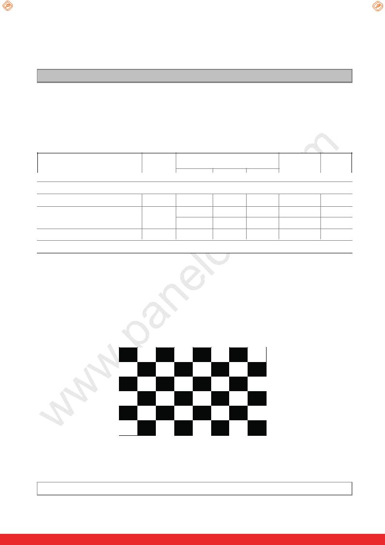
White : 255Gray
Black : 0Gray
Mosaic Pattern(8 x 6)
Ver. 1.0 |
6 /34 |
|
|
One step solution for LCD / PDP / OLED panel application: Datasheet, inventory and accessory! www.panelook.com

Global LCD Panel Exchange Center |
www.panelook.com |
LC320EXJ
Product Specification
3-2. Interface Connections
3-2-1. LCD Module
-LCD Connector(CN1) : KDF71G-30S-1H(Hirose) or FI-X30SSL-HF(JAE)
-Mating Connector : : FI-X30C2L (Manufactured by JAE) or Equivalente
Table 3. MODULE CONNECTOR(CN5) PIN CONFIGURATION
Pin No. |
Symbol |
Description |
Note |
1 |
VLCD |
Power Supply +12.0V |
|
2 |
VLCD |
Power Supply +12.0V |
|
3 |
VLCD |
Power Supply +12.0V |
|
4 |
VLCD |
Power Supply +12.0V |
|
5 |
GND |
Ground |
|
6 |
GND |
Ground |
|
7 |
GND |
Ground |
|
8 |
GND |
Ground |
|
9 |
LVDS Select |
H =JEIDA , L or NC = VESA |
Appendix IV |
10 |
uj |
No Connection |
4 |
11 |
GND |
Ground |
|
12 |
RA- |
LVDS Receiver Signal(-) |
|
13 |
RA+ |
LVDS Receiver Signal(+) |
|
14 |
GND |
Ground |
|
15 |
RB- |
LVDS Receiver Signal(-) |
|
16 |
RB+ |
LVDS Receiver Signal(+) |
|
17 |
GND |
Ground |
|
18 |
RC- |
LVDS Receiver Signal(-) |
|
19 |
RC+ |
LVDS Receiver Signal(+) |
|
20 |
GND |
Ground |
|
21 |
RCLK- |
LVDS Receiver Clock Signal(-) |
|
22 |
RCLK+ |
LVDS Receiver Clock Signal(+) |
|
23 |
GND |
Ground |
|
24 |
RD- |
LVDS Receiver Signal(-) |
|
25 |
RD+ |
LVDS Receiver Signal(+) |
|
26 |
GND |
Ground |
|
27 |
uj |
No Connection |
4 |
28 |
uj |
No Connection |
4 |
29 |
uj |
No Connection |
4 |
30 |
GND |
Ground |
|
Notes : 1. All GND (Ground) pins should be connected together to the LCD module’s metal frame.

 2. All VLCD (power input) pins should be connected together.

 3. All Input levels of LVDS signals are based on the EIA 644 Standard.
 4. These pins are used only for LGD (Do not connect)
5.Specific pin No. #30 is used for “No signal detection” of system signal interface.
It should be GND for NSB (No Signal Black) while the system interface signal is not. If this pin is “H”, LCD Module displays AGP (Auto Generation Pattern).
Ver. 1.0 |
7 /34 |
|
|
One step solution for LCD / PDP / OLED panel application: Datasheet, inventory and accessory! www.panelook.com
Global LCD Panel Exchange Center |
www.panelook.com |
LC320EXJ
Product Specification
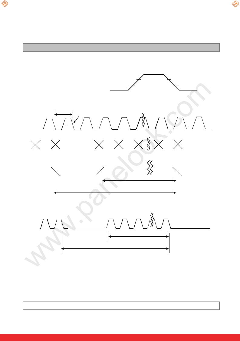
3-3. Signal Timing Specifications
Table 4 shows the signal timing required at the input of the LVDS transmitter. All of the interface signal timings should be satisfied with the following specification for normal operation.
{ G[UGG{ptpunG{hislGOklGv Gt P |
|
|
|
|
|
|||
ITEM |
|
Symbol |
Min |
Typ |
Max |
Unit |
Note |
|
|
Display |
tHV |
- |
1366 |
- |
tclk |
|
|
|
Period |
|
||||||
|
|
|
|
|
|
|
||
Horizontal |
Blank |
tHB |
90 |
162 |
410 |
tclk |
|
|
|
Total |
tHP |
1456 |
1528 |
1776 |
tclk |
|
|
|
Display |
tVV |
- |
768 |
- |
tHP |
|
|
|
Period |
|
||||||
|
|
|
|
|
|
|
||
Vertical |
Blank |
tVB |
20 |
22 |
240 |
tHP |
1 |
|
(126) |
(180) |
(295) |
||||||
|
|
|
|
|
||||
|
Total |
tVP |
788 |
790 |
1008 |
tHP |
|
|
|
(894) |
(948) |
(1063) |
|
||||
|
|
|
|
|
||||
ITEM |
|
Symbol |
Min |
Typ |
Max |
Unit |
Note |
|
|
DCLK |
fCLK |
63.0 |
72.4 |
80.0 |
MHz |
|
|
|
Horizontal |
fH |
45 |
47.4 |
55 |
KHz |
2 |
|
Frequency |
|
|
57 |
60 |
63 |
|
2 |
|
|
Vertical |
fV |
Hz |
NTSC : |
||||
|
(47) |
(50) |
(53) |
57~63Hz |
||||
|
|
|
|
|||||
|
|
|
|
|
|
|
(PAL : 47~53Hz) |
|
Note: 1. The input of HSYNC & VSYNC signal does not have an effect on normal operation (DE Only Mode). If you use spread spectrum of EMI, add some additional clock to minimum value for clock margin.
2. The performance of the electro-optical characteristics may be influenced by variance of the vertical  refresh rate and the horizontal frequency


 Timing should be set based on clock frequency.
Ver. 1.0 |
8 /34 |
|
|
One step solution for LCD / PDP / OLED panel application: Datasheet, inventory and accessory! www.panelook.com
Global LCD Panel Exchange Center |
www.panelook.com |
LC320EXJ
Product Specification
3-4. Signal Timing Waveforms
3-4-1. LVDS Input Signal Timing Diagram
0.7VDD
DE, Data
0.3VDD
DCLK |
tCLK |
0.5 Vcc |
|
|
|
|
|
|
|
|
|
|
|
|
Valid data |
|
|
|
|
|
|
|
|
|
|
|
||
|
|
|
|
|
|
|
|
|
|
|
|
|
|
|
|
|
|
|
|
|
|
|||
|
1366 |
|
|
|
Invalid data |
|
|
|
1 |
|
|
|
|
|
|
1366 |
|
|
|
Invalid data |
||||
|
|
|
|
|
|
|
|
|
|
|
|
|
|
|
|
|
|
|
|
|
|
|
|
|
|
|
|
|
|
|
DE(Data Enable) |
|
|
|
|
|
|
|
|
|
|
|
|
|
|
|
|
|
|
|
|
|
|
|
|
|
|
|
|
|
|
|
|
|
|
|
|
|
|
|
||||
|
|
|
|
|
|
|
|
|
|
|
|
|
|
tHV |
|
|
|
|
|
|||||
|
|
|
|
|
|
|
|
|
|
|
|
|
|
|
|
|
|
|
||||||
|
|
|
|
|
|
|
|
|
|
|
|
|
|
|
|
|
|
|
|
|
|
|||
|
|
|
|
|
|
|
|
|
tHT |
|
|
|
|
|
|
|
|
|
|
|
||||
|
|
|
|
|
|
|
|
|
|
|
|
|
|
|
|
|
|
|
|
|
||||
DE(Data Enable) |
|
|
|
|
|
|
|
|
|
|
|
|
|
|
|
|
|
|
||||||
|
|
|
|
|
|
|
|
|
|
|
|
|
|
|
|
|
|
|||||||
|
|
|
768 |
1 |
|
|
768 |
|
|
|
|
|
|
|||||||||||
tVV
tVT
Ver. 1.0 |
9 /34 |
|
|
One step solution for LCD / PDP / OLED panel application: Datasheet, inventory and accessory! www.panelook.com
Global LCD Panel Exchange Center |
www.panelook.com |
LC320EXJ
Product Specification
3-4-2. LVDS Input Signal Characteristics
1) DC Specification
LVDS |
- |
|
|
|
|
|
|
|
|
LVDS |
+ |
|
|
|
|
|
|
|
|
|
|
|
|
|
|
V CM |
V IN _ MAX V IN _ MIN |
||
|
# V CM = {(LVDS |
+) + ( LVDS - )}/2 |
|
|
|
|
|
|
|
0V |
|
|
|
|
|
|
|
|
|
|
|
|
|
|
|
|
|
|
|
Description |
|
Symbol |
Min |
Max |
|
Unit |
|
Note |
|
LVDS Common mode Voltage |
|
VCM |
1.0 |
1.5 |
|
V |
|
- |
|
LVDS Input Voltage Range |
|
VIN |
0.7 |
1.8 |
|
V |
|
- |
|
Change in common mode Voltage |
|
VCM |
- |
250 |
|
mV |
|
- |
|
|
|
|
|
|
|
|
|
|
|
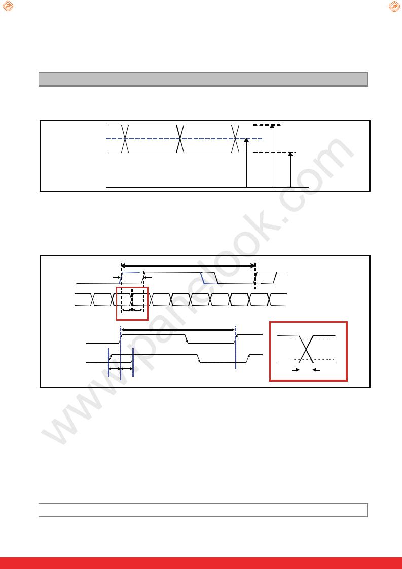
2) AC Specification
Tclk
LVDS Clock
|
A |
|
|
|
|
|
|
|
|
|
|
LVDS Data |
|
|
|
|
|
|
|
|
|
|
|
|
|
|
(Fclk = 1/Tclk ) |
|
|
|
|
A |
|||
|
|
|
Tclk |
|
|
|
|
|
|||
LVDS 1’st Clock |
|
|
|
|
|
|
|
80% |
|||
|
|
|
|
|
|
||||||
|
|
|
|
|
|
|
|
||||
LVDS 2nd / 3rd / 4th Clock |
|
|
|
|
|
|
|
|
|
|
|
|
|
|
|
|
|
|
|
|
|
20% |
|
tSKEW_min tSKEW_max |
|
|
|
|
|
|
|
|
|
tRF |
|
|
|
|
|
|
|
|
|
|
|||
|
|
|
|
|
|
|
|
|
|
||
Description |
|
Symbol |
Min |
Max |
Unit |
|
|
Note |
|||
LVDS Differential Voltage |
High Threshold |
|
VTH |
100 |
300 |
mV |
|
|
3 |
||
Low Threshold |
|
VTL |
-300 |
-100 |
mV |
|
|
||||
|
|
|
|
|
|
||||||
LVDS Clock to Data Skew |
|
tSKEW |
- |
|(0.20*Tclk)/7| |
ps |
|
|
- |
|||
LVDS Clock/DATA Rising/Falling time |
|
tRF |
260 |
|(0.3*Tclk)/7| |
ps |
|
|
2 |
|||
Effective time of LVDS |
|
teff |
|·360| |
- |
ps |
|
|
- |
|||
LVDS Clock to Clock Skew (Even to Odd) |
|
tSKEW_EO |
- |
|1/7* Tclk| |
ps |
|
|
- |
|||
Note 1. All Input levels of LVDS signals are based on the EIA 644 Standard.
2.If tRF isn’t enough, teff should be meet the range.
3.LVDS Differential Voltage is defined within teff
Ver. 1.0 |
10 /34 |
|
|
One step solution for LCD / PDP / OLED panel application: Datasheet, inventory and accessory! www.panelook.com
Global LCD Panel Exchange Center |
www.panelook.com |
LC320EXJ
Product Specification
|
360ps |
|
0.5tui |
tui |
|
V+ |
|
|
data |
|
|
|
VTH |
|
Vcm |
|
|
|
VTL |
|
V- |
360ps |
|
data |
||
|
||
|
teff |
|
V+ |
tui : Unit Interval |
|
clk |
|
|
Vcm |
|
|
V- |
|
|
clk |
|
Ver. 1.0 |
11 /34 |
|
|
One step solution for LCD / PDP / OLED panel application: Datasheet, inventory and accessory! www.panelook.com
 Loading...