


LM230WF3
Liquid Crystal Display
Product Specification
SPECIFICATION
FOR
APPROVAL
( ● ) Preliminary Specification
( ) Final Specification
Title  23” Full HD TFT LCD
BUYER
MODEL
General
SUPPLIER |
LG Display Co., Ltd. |
*MODEL |
LM230WF3 |
SUFFIX |
SLK1 |
*When you obtain standard approval,
please use the above model name without suffix
APPROVED BY |
SIGNATURE |
|
DATE |
||
|
||
/ |
|
/
/
Please return 1 copy for your confirmation with your signature and comments.
APPROVED BY |
SIGNATURE |
|
DATE |
||
|
C.K. Lee / G.Manager
REVIEWED BY
J.H. Song / Manager [C]
S.Y. An / Manager [M]
C.S. Shin / Manager [P]
PREPARED BY
D.G. Lee / Engineer
MNT Products Engineering Dept.
LG Display Co., Ltd
Ver. 0.0 |
July., 24, 2012 |
1 / 32 |
|
|
|
PDF created with pdfFactory Pro trial version www.pdffactory.com
LM230WF3
Liquid Crystal Display
Product Specification
Contents
No |
ITEM |
Page |
|
|
|
|
COVER |
1 |
|
CONTENTS |
2 |
|
RECORD OF REVISIONS |
3 |
1 |
GENERAL DESCRIPTION |
4 |
2 |
ABSOLUTE MAXIMUM RATINGS |
5 |
3 |
ELECTRICAL SPECIFICATIONS |
6 |
|
|
|
3-1 |
ELECTRICAL CHARACTREISTICS |
6 |
3-2 |
INTERFACE CONNECTIONS |
9 |
3-3 |
SIGNAL TIMING SPECIFICATIONS |
14 |
3-4 |
SIGNAL TIMING WAVEFORMS |
15 |
3-5 |
COLOR INPUT DATA REFERNECE |
16 |
3-6 |
POWER SEQUENCE |
17 |
3-7 VLCD Power Dip Condition |
18 |
|
4 |
OPTICAL SPECIFICATIONS |
19 |
5 |
MECHANICAL CHARACTERISTICS |
25 |
6 |
RELIABLITY |
28 |
7 |
INTERNATIONAL STANDARDS |
29 |
7-1 |
SAFETY |
29 |
7-2 |
EMC |
29 |
7-3 |
ENVIRONMENT |
29 |
8 |
PACKING |
30 |
8-1 |
DESIGNATION OF LOT MARK |
30 |
8-2 |
PACKING FORM |
30 |
9 |
PRECAUTIONS |
31 |
Ver. 0.0 |
July., 24, 2012 |
2 / 32 |
|
|
|
PDF created with pdfFactory Pro trial version www.pdffactory.com

LM230WF3
Liquid Crystal Display
|
|
|
|
Product Specification |
|
|
|
|
RECORD OF REVISIONS |
|
|
|
|
|
|
|
|
|
Revision |
Revision |
Page |
Description |
|
|
No |
Date |
|
||
|
|
|
|
||
|
|
|
|
|
|
0.0 |
July., 24, 2012 |
- |
First Draft, Preliminary Specifications |
|
|
Ver. 0.0 |
July., 24, 2012 |
3 / 32 |
|
|
|
PDF created with pdfFactory Pro trial version www.pdffactory.com
LM230WF3
Liquid Crystal Display
Product Specification
1. General Description
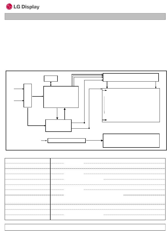
LM230WF3 is a Color Active Matrix Liquid Crystal Display with a Light Emitting Diode ( White LED) backlight
system without LED driver. The matrix employs a-Si Thin Film Transistor as |
the active element. |
It is a transmissive type display operating in the normally black mode. It has a 23 inch |
diagonally measured |
active display area with FHD resolution (1080 vertical by 1920horizontal pixel array) Each pixel is divided into Red, Green and Blue sub-pixels or dots which are arranged in vertical stripes. Gray scale or the brightness of the sub-pixel color is determined with a 8-bit gray scale signal for each dot, thus, presenting a palette of more than 16,7M colors with A-FRC (Advanced Frame Rate Control).
It has been designed to apply the 8Bit 2 port LVDS interface.
It is intended to support displays where high brightness, super wide viewing angle, high color saturation, and high color are important.
RGB
EEPROM
Source Driver Circuit
LVDS |
I2C |
S1 |
S1920 |
|
|||
|
|
|
2port |
|
|
|
G1 |
|
|
|
CN1 |
Timing |
|
|
|
|
||
|
|
|
|
|
|||
(30pin) |
Controller |
|
|
|
|
|
|
|
|
|
TFT - LCD Panel |
|
|
||
+5.0V |
|
|
|
|
|
|
|
|
|
|
|
|
|
|
|
|
Logic Power |
|
|
(1920 × RGB × 1080 pixels) |
|
|
|
|
|
|
|
|
|
||
|
|
|
|
G1080 |
|
|
|
+5.0V |
|
|
|
|
|
|
|
Power Circuit |
|
|
|
|
|
|
|
|
|
|
|
|
|
||
|
|
|
|
|
|
||
|
Block |
|
|
|
|
|
|
|
|
|
|
|
|
|
|
|
|
|
|
|
|
|
|
VLED |
CN2 (6PIN) |
|
Back light Assembly |
|
|
||
|
(LED) |
|
|
||||
|
|
|
|
|
|
|
|
|
|
|
|
|
|
|
|
General Features |
[ Figure 1 ] Block diagram |
|
|
|
|||
|
|
|
|
|
|
|
|
Active Screen Size |
23 inches(58.42cm) diagonal |
|
|
|
|
||
Outline Dimension |
533.2(H) x 312.0(V) x 10.5(D) mm (Typ.) |
|
|
||||
Pixel Pitch |
0.2652 mm x 0.2652 mm |
|
|
|
|
||
Pixel Format |
1920 horiz. By 1080 vert. Pixels RGB stripes arrangement |
|
|
||||
Color Depth |
16,7M colors (6bit + A-FRC) |
|
|
|
|
||
Luminance, White |
250 cd/m2 ( Center 1 Point, Typ.) |
|
|
|
|
||
Viewing Angle(CR>10) |
View Angle Free (R/L 178(Typ.), U/D 178(Typ.)) |
|
|
||||
Power Consumption |
Total (15.9) Watt (Typ.) ( (4.0) Watt @VLCD, (11.9W) Watt @Is=120mA ) |
||||||
Weight |
(2190)g (typ.) |
|
|
|
|
||
Display Operating Mode |
Transmissive mode, normally black |
|
|
|
|||
Surface Treatment |
Hard coating(3H), Anti-glare treatment of the front polarizer |
|
|
||||
|
|
|
|
|
|
|
|
Ver. 0.0 |
|
July., 24, 2012 |
|
|
4 / 32 |
||
|
|
|
|
|
|
|
|
PDF created with pdfFactory Pro trial version www.pdffactory.com
LM230WF3
Liquid Crystal Display
Product Specification
2. Absolute Maximum Ratings
The following are maximum values which, if exceeded, may cause faulty operation or damage to the unit.
Table 1. ABSOLUTE MAXIMUM RATINGS
Parameter |
Symbol |
|
Values |
Units |
Notes |
|
Min |
Max |
|||||
|
|
|
|
|||
|
|
|
|
|
|
|
Power Input Voltage |
VLCD |
-0.3 |
6.0 |
Vdc |
at 25 ± 2°C |
|
Operating Temperature |
TOP |
0 |
50 |
°C |
|
|
Storage Temperature |
TST |
-20 |
60 |
°C |
1, 2, 3 |
|
Operating Ambient Humidity |
HOP |
10 |
90 |
%RH |
||
|
||||||
Storage Humidity |
HST |
10 |
90 |
%RH |
|
|
LCM Surface Temperature |
TSurface |
0 |
65 |
|
1, 4 |
|
(Operation) |
||||||
|
|
|
|
|
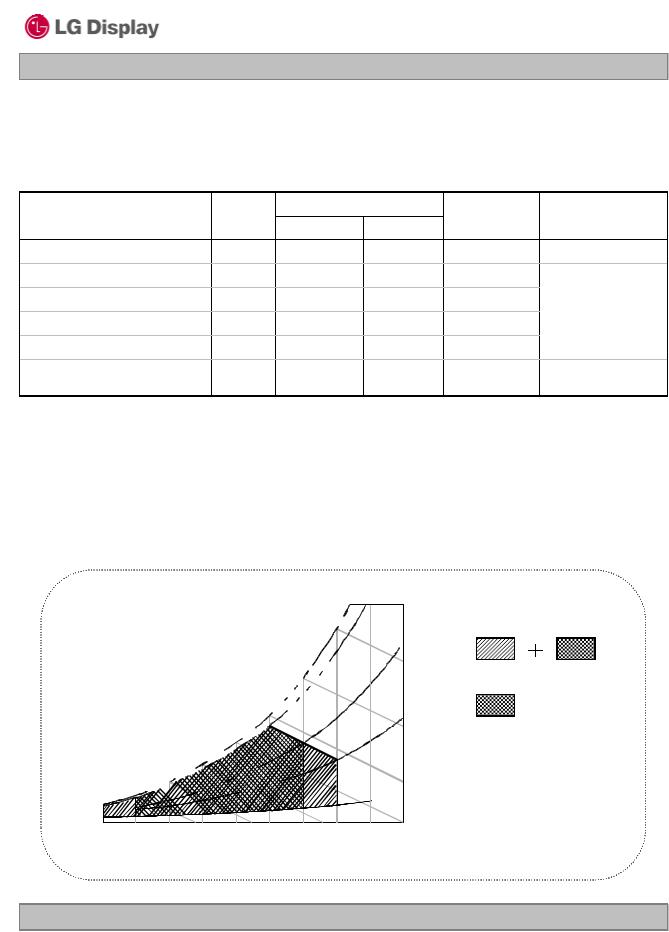
Note : 1. Temperature and relative humidity range are shown in the figure below. Wet bulb temperature should be 39 °C Max, and no condensation of water.
2.Maximum Storage Humidity is up to 40 , 70% RH only for 4 corner light leakage Mura.
3.Storage condition is guaranteed under packing condition
4.LCM Surface Temperature should be Min. 0 and Max. 65 under the VLCD=5.0V,
fV=60Hz, 25 ambient Temp. no humidity control and LED string current is typical value.
FIG.2 Temperature and relative humidity
60 
50 
 Wet Bulb


Temperature [C] 
 40
40


30


20


10 


 0
0


90%
 60%
60%
[(%)RH] 40% Humidity


 10%
10%
Storage
Operation
-20 |
0 |
10 |
20 |
30 |
40 |
50 |
60 |
70 |
80 |
|
|
Dry Bulb Temperature [C] |
|
|
|
|
|||
Ver. 0.0 July., 24, 2012 5 / 32
PDF created with pdfFactory Pro trial version www.pdffactory.com
LM230WF3
Liquid Crystal Display
Product Specification
3. Electrical Specifications
3-1. Electrical Characteristics
It requires two power inputs. One is employed to power the LCD electronics and to drive the TFT array and liquid crystal. The second input power for the LED/Backlight, is typically generated by a LED Driver.
The LED Driver is an external unit to the LCDs.
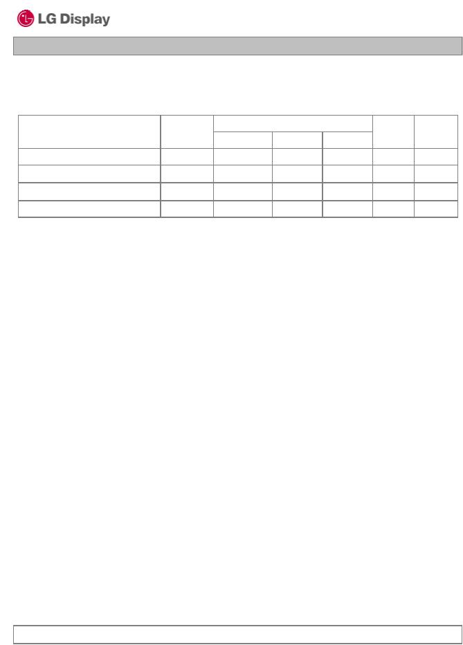
Table 2-1. ELECTRICAL CHARACTERISTICS
Parameter |
Symbol |
|
Values |
|
Unit |
Notes |
|
Min |
Typ |
Max |
|||||
|
|
|
|
||||
|
|
|
|
|
|
|
|
MODULE : |
|
|
|
|
|
|
|
Power Supply Input Voltage |
VLCD |
4.5 |
5 |
5.5 |
Vdc |
|
|
Permissive Power Input Ripple |
VdRF |
|
|
100 |
mVp-p |
1 |
|
Power Supply Input Current |
ILCD |
- |
(790) |
(990) |
mA |
2 |
|
- |
(960) |
(1200) |
mA |
3 |
|||
|
|
||||||
Power Consumption |
Pc TYP |
- |
(4.0) |
(5.0) |
Watt |
2 |
|
Pc MAX |
- |
(4.8) |
(6.0) |
Watt |
3 |
||
|
|||||||
Rush current |
IRUSH |
- |
- |
3.0 |
A |
4 |
Note :
1.Permissive power ripple should be measured under VLCD =5.0V, 25°C, fV(frame frequency)=MAX condition and At that time, we recommend the bandwidth configuration of oscilloscope is to be under 20Mhz. See the next page.
2.The specified current and power consumption are under the VLCD=5.0V, 25± 2°C,fV=60Hz condition whereas Typical Power Pattern [Mosaic] shown in the [ Figure 3 ] is displayed.
3.The current is specified at the maximum current pattern.
4.Maximum Condition of Inrush current :
The duration of rush current is about 5ms and rising time of power Input is 500us ± 20%.(min.).
Ver. 0.0 |
July., 24, 2012 |
6 / 32 |
|
|
|
PDF created with pdfFactory Pro trial version www.pdffactory.com
LM230WF3
Liquid Crystal Display
Product Specification
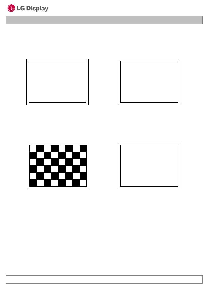
• Permissive Power input ripple (VLCD =5.0V, 25°C, fv (frame frequency)=MAX condition)
|
|
White pattern |
Black pattern |
• Power consumption (VLCD =5V, 25°C, fV (frame frequency=60Hz condition)
Typical power Pattern Maximum power Pattern
FIG.3 Mosaic pattern & White Pattern for power consumption measurement
Ver. 0.0 |
July., 24, 2012 |
7 / 32 |
|
|
|
PDF created with pdfFactory Pro trial version www.pdffactory.com
LM230WF3
Liquid Crystal Display
Product Specification
Table 2-2. LED Bar ELECTRICAL CHARACTERISTICS
Parameter |
Symbol |
|
Values |
|
Unit |
Notes |
|
Min. |
Typ. |
Max. |
|||||
|
|
|
|
||||
|
|
|
|
|
|
|
|
LED String Current |
Is |
- |
120 |
TBD |
mA |
1, 2, 5 |
|
LED String Voltage |
Vs |
(46.4) |
(49.6) |
(52.8) |
V |
1, 5 |
|
Power Consumption |
PBar |
- |
(11.9) |
TBD |
Watt |
1, 2, 4 |
|
LED Life Time |
LED_LT |
30,000 |
- |
- |
Hrs |
3 |
Notes) The LED Bar consists of 32 LED packages, 2 strings (parallel) x 16 packages (serial)
LED driver design guide
:The design of the LED driver must have specifications for the LED in LCD Assembly.
The performance of the LED in LCM, for example life time or brightness, is extremely influenced by the characteristics of the LED driver.
So all the parameters of an LED driver should be carefully designed and output current should be Constant current control.
Please control feedback current of each string individually to compensate the current variation among the strings of LEDs.
When you design or order the LED driver, please make sure unwanted lighting caused by the mismatch of the LED and the LED driver (no lighting, flicker, etc) never occurs.
When you confirm it, the LCD module should be operated in the same condition as installed in your instrument.
1.The specified values are for a single LED bar.
2.The specified current is defined as the input current for a single LED string with 100% duty cycle.
3.The LED life time is defined as the time when brightness of LED packages become 50% or less than the initial value under the conditions at Ta = 25 ± 2°C and LED string current is typical value.
4.The power consumption shown above does not include loss of external driver.
The typical power consumption is calculated as PBar = Vs(Typ.) x Is(Typ.) x No. of strings. The maximum power consumption is calculated as PBar = Vs(Max.) x Is(Typ.) x No. of strings.
5.LED operating conditions are must not exceed Max. ratings.
Ver. 0.0 |
July., 24, 2012 |
8 / 32 |
|
|
|
PDF created with pdfFactory Pro trial version www.pdffactory.com
LM230WF3
Liquid Crystal Display
Product Specification
3-2. Interface Connections
3-2-1. LCD Module
-LCD Connector(CN1) : IS100-L30O-C23 (UJU) , GT103-30S-HF15 (LSM)
-Mating Connector : FI-X30C2L (Manufactured by JAE) or Equivalent
Table 3. MODULE CONNECTOR(CN1) PIN CONFIGURATION
No |
Symbol |
Description |
No |
Symbol |
Symbol |
|
|
|
|
|
|
1 |
FR0M |
Minus signal of odd channel 0 (LVDS) |
16 |
SR1P |
Plus signal of even channel 1 (LVDS) |
2 |
FR0P |
Plus signal of odd channel 0 (LVDS) |
17 |
GND |
Ground |
3 |
FR1M |
Minus signal of odd channel 1 (LVDS) |
18 |
SR2M |
Minus signal of even channel 2 (LVDS) |
4 |
FR1P |
Plus signal of odd channel 1 (LVDS) |
19 |
SR2P |
Plus signal of even channel 2 (LVDS) |
5 |
FR2M |
Minus signal of odd channel 2 (LVDS) |
20 |
SCLKINM |
Minus signal of even clock channel (LVDS) |
6 |
FR2P |
Plus signal of odd channel 2 (LVDS) |
21 |
SCLKINP |
Plus signal of even clock channel (LVDS) |
7 |
GND |
Ground |
22 |
SR3M |
Minus signal of even channel 3 (LVDS) |
8 |
FCLKINM |
Minus signal of odd clock channel (LVDS) |
23 |
SR3P |
Plus signal of even channel 3 (LVDS) |
9 |
FCLKINP |
Plus signal of odd clock channel (LVDS) |
24 |
GND |
Ground |
10 |
FR3M |
Minus signal of odd channel 3 (LVDS) |
25 |
NC |
No Connection (I2C Serial interface for LCM) |
11 |
FR3P |
Plus signal of odd channel 3 (LVDS) |
26 |
NC |
No Connection.(I2C Serial interface for LCM) |
12 |
SR0M |
Minus signal of even channel 0 (LVDS) |
27 |
ITLC |
Interlace Mode Selection |
13 |
SR0P |
Plus signal of even channel 0 (LVDS) |
28 |
VLCD |
Power Supply +5.0V |
14 |
GND |
Ground |
29 |
VLCD |
Power Supply +5.0V |
15 |
SR1M |
Minus signal of even channel 1 (LVDS) |
30 |
VLCD |
Power Supply +5.0V |
Note: 1. All GND(ground) pins should be connected together and to Vss which should also be connected to the LCD’s metal frame.
2.All VLCD (power input) pins should be connected together.
3.Input Level of LVDS signal is based on the IEA 664 Standard.
4.ITLC is Interlace mode selection pin. (L : Normal Mode, H : Interlace Mode) If you don’t use this pin, it should be connected to GND.
|
|
|
|
#1 IS100-L30O-C23 |
#30 |
|
#1 |
#30 |
|
|
|
||||||||||||||||||||||||||||||||||
|
|
|
|
|
|
|
|
|
|
|
|
|
|||||||||||||||||||||||||||||||||
|
|
|
|
|
|
|
|
|
|
|
|
|
|||||||||||||||||||||||||||||||||
|
|
|
|
|
|
|
|
|
|
|
|
|
|
|
|
|
|
|
|
|
|
|
|
|
|
|
|
|
|
|
|
|
|
|
|
|
|
|
|
|
|
Rear view of LCM |
|
|
|
|
|
|
|
|
|
|
|
|
|
|
|
|
|
|
|
|
|
|
|
|
|
|
|
|
|
|
|
|
|
|
|
|
|
|
|
|
|
|
|
|
|
||||
|
|
|
|
|
|
|
|
|
|
|
|
|
|
|
|
|
|
|
|
|
|
|
|
|
|
|
|
|
|
|
|
|
|
|
|
|
|
|
|
|
|
||||
|
|
|
|
|
|
|
|
|
|
|
|
|
|
|
|
|
|
|
|
|
|
|
|
|
|
|
|
|
|
|
|
|
|
|
|
|
|
|
|
|
|
||||
|
|
|
|
|
|
|
|
|
|
|
|
|
|
|
|
|
|
|
|
|
|
|
|
|
|
|
|
|
|
|
|
FIG.4 Connector diagram |
|
|
|
|
|||||||||
|
|
|
|
|
|
|
|
|
|
|
|
|
|
|
|
|
|
|
|
|
|
|
|
|
|
|
|
|
|
|
|
|
|
|
|
|
|
|
|
|
|
|
|
|
|
Ver. 0.0 |
|
|
|
|
|
July., 24, 2012 |
9 / 32 |
||||||||||||||||||||||||||||||||||||||
|
|
|
|
|
|
|
|
|
|
|
|
|
|
|
|
|
|
|
|
|
|
|
|
|
|
|
|
|
|
|
|
|
|
|
|
|
|
|
|
|
|
|
|
|
|
PDF created with pdfFactory Pro trial version www.pdffactory.com
|
|
|
|
|
|
|
LM230WF3 |
|
|
|
|
|
|
|
|
Liquid Crystal Display |
|
|
|
|
|
|
|
|
|
|
|
|
|
|
Product Specification |
|
|
||
|
Table 4. REQUIRED SIGNAL ASSIGNMENT FOR Flat Link (TI:SN75LVDS83) Transmitter |
|
||||||
|
|
|
|
|
|
|
||
|
Pin # |
Pin Name |
Require Signal |
Pin # |
Pin Name |
Require Signal |
|
|
|
|
|
|
|
|
|
|
|
1 |
|
VCC |
Power Supply for TTL Input |
29 |
GND |
Ground pin for TTL |
|
|
2 |
|
D5 |
TTL Input (R7) |
30 |
D26 |
TTL Input (DE) |
|
|
3 |
|
D6 |
TTL Input (R5) |
31 |
TX CLKIN |
TTL Level clock Input |
|
|
4 |
|
D7 |
TTL Input (G0) |
32 |
PWR DWN |
Power Down Input |
|
|
5 |
|
GND |
Ground pin for TTL |
33 |
PLL GND |
Ground pin for PLL |
|
|
6 |
|
D8 |
TTL Input (G1) |
34 |
PLL VCC |
Power Supply for PLL |
|
|
7 |
|
D9 |
TTL Input (G2) |
35 |
PLL GND |
Ground pin for PLL |
|
|
8 |
|
D10 |
TTL Input (G6) |
36 |
LVDS GND |
Ground pin for LVDS |
|
|
9 |
|
VCC |
Power Supply for TTL Input |
37 |
TxOUT3 |
Positive LVDS differential data output 3 |
|
|
10 |
|
D11 |
TTL Input (G7) |
38 |
TxOUT3 |
Negative LVDS differential data output 3 |
|
|
11 |
|
D12 |
TTL Input (G3) |
39 |
TX CLKOUT |
Positive LVDS differential clock output |
|
|
12 |
|
D13 |
TTL Input (G4) |
40 |
TX CLKOUT |
Negative LVDS differential clock output |
|
|
13 |
|
GND |
Ground pin for TTL |
41 |
TX OUT2 |
Positive LVDS differential data output 2 |
|
|
14 |
|
D14 |
TTL Input (G5) |
42 |
TX OUT2 |
Negative LVDS differential data output 2 |
|
|
15 |
|
D15 |
TTL Input (B0) |
43 |
LVDS GND |
Ground pin for LVDS |
|
|
16 |
|
D16 |
TTL Input (B6) |
44 |
LVDS VCC |
Power Supply for LVDS |
|
|
17 |
|
VCC |
Power Supply for TTL Input |
45 |
TX OUT1 |
Positive LVDS differential data output 1 |
|
|
18 |
|
D17 |
TTL Input (B7) |
46 |
TX OUT1 |
Negative LVDS differential data output 1 |
|
|
19 |
|
D18 |
TTL Input (B1) |
47 |
TX OUT0 |
Positive LVDS differential data output 0 |
|
|
20 |
|
D19 |
TTL Input (B2) |
48 |
TX OUT0 |
Negative LVDS differential data output 0 |
|
|
21 |
|
GND |
Ground pin for TTL Input |
49 |
LVDS GND |
Ground pin for LVDS |
|
|
22 |
|
D20 |
TTL Input (B3) |
50 |
D27 |
TTL Input (R6) |
|
|
23 |
|
D21 |
TTL Input (B4) |
51 |
D0 |
TTL Input (R0) |
|
|
24 |
|
D22 |
TTL Input (B5) |
52 |
D1 |
TTL Input (R1) |
|
|
25 |
|
D23 |
TTL Input (RSVD) |
53 |
GND |
Ground pin for TTL |
|
|
26 |
|
VCC |
Power Supply for TTL Input |
54 |
D2 |
TTL Input (R2) |
|
|
27 |
|
D24 |
TTL Input (HSYNC) |
55 |
D3 |
TTL Input (R3) |
|
|
28 |
|
D25 |
TTL Input (VSYNC) |
56 |
D4 |
TTL Input (R4) |
|
|
|
Notes : |
1. Refer to LVDS Transmitter Data Sheet for detail descriptions. |
|
|||||
|
|
|
2. 7 means MSB and 0 means LSB at R,G,B pixel data |
|
|
|||
|
|
|
|
|
|
|
||
|
Ver. 0.0 |
|
July., 24, 2012 |
10 / 32 |
|
|||
|
|
|
|
|
|
|
|
|
PDF created with pdfFactory Pro trial version www.pdffactory.com
 Loading...