


LC420DUJ
Product Specification
SPECIFICATION
FOR
APPROVAL
( ● ) |
Preliminary Specification |
|
|
( ) |
Final Specification |
|
|
|
|
|
|
|
Title |
|
42.0” WUXGA TFT LCD |
BUYER GENERAL
MODEL
SUPPLIER |
LG.Display Co., Ltd. |
|
|
*MODEL |
LC420DUJ |
|
|
SUFFIX |
SGE1 (RoHS Verified) |
|
|
*When you obtain standard approval,
please use the above model name without suffix
APPROVED BY |
|
SIGNATURE |
|
DATE |
|
|
|
|
/ |
|
|
|
|
|
/
/
Please return 1 copy for your confirmation with your signature and comments.
APPROVED BY |
|
SIGNATURE |
|
DATE |
|
|
|
|
Y.J. Heo / Team Leader |
|
|
|
|
|
REVIEWED BY |
|
|
Q.H. Joe / Project Leader |
|
|
|
|
|
PREPARED BY |
|
|
M.S. Park / Engineer |
|
|
|
|
|
TV Products Development Dept.
LG. Display LCD Co., Ltd
Ver. 0.1 |
0 /43 |
|
|
PDF created with pdfFactory Pro trial version www.pdffactory.com
|
|
LC420DUJ |
|
Product Specification |
|
|
CONTENTS |
|
|
|
|
Number |
ITEM |
Page |
|
COVER |
0 |
|
CONTENTS |
1 |
|
RECORD OF REVISIONS |
2 |
1 |
GENERAL DESCRIPTION |
3 |
2 |
ABSOLUTE MAXIMUM RATINGS |
4 |
3 |
ELECTRICAL SPECIFICATIONS |
5 |
3-1 |
ELECTRICAL CHARACTERISTICS |
5 |
3-2 |
INTERFACE CONNECTIONS |
6 |
3-3 |
SIGNAL TIMING SPECIFICATIONS |
7 |
3-4 |
LVDS SIGNAL SPECIFICATIONS |
9 |
3-5 |
INTARA INTERFACE SIGNAL SPECIFICATION |
12 |
3-6 |
COLOR DATA REFERENCE |
13 |
3-7 |
POWER SEQUENCE |
14 |
4 |
OPTICAL SPECIFICATIONS |
15 |
5 |
MECHANICAL CHARACTERISTICS |
21 |
6 |
MECHANICAL DIMENSION |
22 |
6-1 |
BOARD ASSEMBLY DIMENSION |
22 |
6-2 |
CONTROL BOARD ASSEMBLY DIMMENSION |
23 |
7 |
RELIABILITY |
24 |
8 |
INTERNATIONAL STANDARDS |
25 |
8-1 |
SAFETY |
25 |
8-2 |
ENVIRONMENT |
25 |
9 |
PACKING |
26 |
9-1 |
PACKING FORM |
26 |
10 |
PRECAUTIONS |
27 |
10-1 |
HANDLING PRECAUTIONS |
27 |
10-2 |
OPERATING PRECAUTIONS |
27 |
10-3 |
PROTECTION FILM |
28 |
10-4 |
STORAGE PRECAUTIONS |
28 |
10-5 |
PACKING PRECAUTIONS |
28 |
|
|
|
|
|
|
Ver. 0.1 |
|
1 /43 |
|
|
|
PDF created with pdfFactory Pro trial version www.pdffactory.com
LC420DUJ
|
|
|
Product Specification |
|
|
|
RECORD OF REVISIONS |
||
|
|
|
|
|
Revision No. |
Revision Date |
Page |
|
Description |
|
|
|
|
|
0.1 |
June, 05, 2013 |
- |
|
Preliminary Specification(First Draft) |
|
|
|
|
|
|
|
|
|
|
|
|
|
|
|
|
|
|
|
|
|
|
|
|
|
|
|
|
|
|
|
|
|
|
|
|
|
|
|
|
|
|
|
|
|
|
|
|
|
|
|
|
|
|
|
|
|
|
|
|
|
|
|
|
|
|
|
|
|
|
|
|
|
|
|
|
|
|
|
|
|
|
|
|
|
|
|
|
|
|
|
|
|
|
|
|
|
|
|
|
|
|
|
|
|
|
|
|
|
|
|
|
|
|
|
|
|
|
|
|
|
|
|
|
|
|
|
|
|
|
|
|
|
|
|
|
|
|
|
|
|
|
|
|
|
Ver. 0.1 |
2 /43 |
|
|
PDF created with pdfFactory Pro trial version www.pdffactory.com

LC420DUJ
Product Specification
1. General Description
The LC420DUJ is a Color Active Matrix Liquid Crystal Display with an integral the Source PCB and Gate implanted on Panel (GIP). The matrix employs a-Si Thin Film Transistor as the active element. It is a transmissive type display operating in the normally black mode. It has a 41.92 inch diagonally measured active display area with WUXGA resolution (1080 vertical by 1920 horizontal pixel array). Each pixel is divided into Red, Green and Blue sub-pixels or dots which are arranged in vertical stripes. Gray scale or the luminance of the sub-pixel color is determined with a 8-bit gray scale signal for each dot. Therefore, it can present a palette of more than 16.7M(true) colors.
It is intended to support LCD TV, PCTV where high brightness, super wide viewing angle, high color gamut, high color depth and fast response time are important.
|
|
EEPROM |
EPI(RGB) |
|
|
LVDS |
|
|
Source Driver Circuit |
||
|
|
|
|
||
|
|
|
|
|
|
2Port |
|
SCL |
SDA |
S1 |
S1920 |
|
|
||||
LVDS |
LVDS 1,2 |
|
|
G1 |
|
|
|
|
|
|
|
Select |
Option |
Timing Controller |
|
TFT - LCD Panel |
|
|
LVDS Rx + DGA |
|
|||
CN1 |
signal |
|
|||
Integrated |
|
(1920 × RGB × 1080 pixels) |
|||
(51pin) |
|
|
|
Control |
[Gate In Panel] |
+12.0V |
|
|
|
||
I2C |
|
|
Signals |
|
|
|
|
|
G1080 |
|
|
|
|
|
|
|
|
|
|
Power Circuit |
Power Signals |
|
|
|
|
|
Block |
|
|
General Features
Active Screen Size |
41.92inches(1064.77mm) diagonal |
||
Outline Dimension |
943.6(H) x 538.3 (V) x 1.4 mm(D) (Typ.) |
||
Pixel Pitch |
0.4833 mm x 0.4833 mm |
||
Pixel Format |
1920 |
horiz. by 1080 vert. Pixels, RGB stripe arrangement |
|
Color Depth |
8-bit, |
16.7 M colors |
|
Drive IC Data Interface |
Source D-IC : 8-bit EPI, gamma reference voltage, and control signals |
||
Gate D-IC : Gate In Panel |
|||
|
|||
Transmittance (With POL) |
6.35%(Typ.) |
||
Viewing Angle (CR>10) |
Viewing angle free ( R/L 178 (Min.), U/D 178 (Min.)) |
||
Weight |
1.5Kg (Typ.) |
||
Display Mode |
Transmissive mode, Normally black |
||
Surface Treatment (Top) |
Hard coating(3H), Anti-glare treatment of the front polarizer, Haze 1%(Typ.) |
||
|
|
|
|
|
|
|
|
Ver. 0.1 |
|
3 /43 |
|
|
|
|
|
PDF created with pdfFactory Pro trial version www.pdffactory.com
LC420DUJ
Product Specification
2. Absolute Maximum Ratings
The following items are maximum values which, if exceeded, may cause faulty operation or permanent damage to the LCD module.
Table 1. ABSOLUTE MAXIMUM RATINGS
Parameter |
Symbol |
|
Value |
Unit |
Note |
|||
Min |
|
Max |
||||||
|
|
|
|
|
|
|
||
Power Input Voltage |
|
LCD Circuit |
VLCD |
-0.3 |
|
+14.0 |
VDC |
1 |
|
|
|
|
|
|
|
|
|
T-Con Option Selection Voltage |
VLOGIC |
-0.3 |
|
+4.0 |
VDC |
|
||
Operating Temperature |
|
TOP |
0 |
|
+50 |
°C |
2,3 |
|
Storage Temperature(without packing) |
TST |
-20 |
|
+60 |
°C |
|||
|
|
|||||||
Panel Front Temperature |
|
TSUR |
- |
|
+68 |
°C |
4 |
|
Operating Ambient Humidity |
HOP |
10 |
|
90 |
%RH |
2,3 |
||
Storage Humidity |
|
HST |
5 |
|
90 |
%RH |
||
|
|
|
||||||
|
|
|
|
|
|
|
|
|
Note1. Ambient temperature condition (Ta = 25 ± 2 °C )
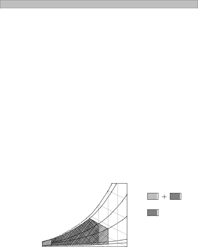
2.Temperature and relative humidity range are shown in the figure below. Wet bulb temperature should be Max 39°C, and no condensation of water.
3.Gravity mura can be guaranteed below 40°C condition.
4.The maximum operating temperatures is based on the test condition that the surface temperature
of display area is less than or equal to 68°C with LCD module alone in a temperature controlled chamber. Thermal management should be considered in final product design to prevent the surface temperature of display area from being over 68 . The range of operating temperature may be degraded in case of improper thermal management in final product design.
|
|
|
|
|
|
|
|
90% |
|
|
|
|
|
|
|
|
|
60 |
|
|
|
|
|
|
|
|
|
|
|
|
60% |
|
|
Wet Bulb |
|
|
|
50 |
|
|
|
Storage |
|
|
|
|
|
|
|
|
|
|
||
|
Temperature [°C] |
|
40 |
|
|
|
Humidity [(%)RH] |
|
||
|
|
|
|
|
|
|
|
|
||
|
|
|
|
|
|
|
|
|
40% |
Operation |
|
|
|
|
30 |
|
|
|
|
|
|
|
|
|
|
|
|
|
|
|
|
|
|
|
|
20 |
|
|
|
|
|
|
|
|
0 |
10 |
|
|
|
|
|
|
|
|
|
|
|
|
|
|
|
|
10% |
|
|
|
|
|
|
|
|
|
|
|
|
|
|
|
|
|
|
|
|
|
|
5% |
|
-20 |
0 |
10 |
20 |
30 |
40 |
50 |
60 |
70 |
80 |
|
|
|
Dry Bulb Temperature [°C] |
|
|
|
|
||||
Ver. 0.1 |
4 /43 |
|
|
PDF created with pdfFactory Pro trial version www.pdffactory.com

LC420DUJ
Product Specification
3. Electrical Specifications
3-1. Electrical Characteristics
Table 2. ELECTRICAL CHARACTERISTICS
Parameter |
Symbol |
|
Value |
|
Unit |
Note |
||
|
|
|
||||||
Min |
Typ |
Max |
||||||
|
|
|
|
|
||||
Circuit : |
|
|
|
|
|
|
|
|
|
|
|
|
|
|
|
|
|
Power Input Voltage |
|
VLCD |
10.8 |
12.0 |
13.2 |
VDC |
|
|
Power Input Current |
|
ILCD |
- |
500 |
650 |
mA |
1 |
|
|
|
|
- |
700 |
910 |
mA |
2 |
|
T-CON Option |
Input High Voltage |
VIH |
1.62 |
- |
1.98 |
VDC |
|
|
Selection Voltage |
Input Low Voltage |
VIL |
0 |
- |
0.54 |
VDC |
|
|
Power Consumption |
|
PLCD |
- |
6 |
7.8 |
Watt |
1 |
|
Rush current |
|
IRUSH |
- |
- |
5.0 |
A |
3 |
|
|
|
|
|
|
|
|
|
|
Note 1. The specified current and power consumption are under the VLCD=12.0V, Ta=25 ± 2°C, fV=60Hz condition, and mosaic pattern(8 x 6) is displayed and fV is the frame frequency.
2. The current is specified at the maximum current pattern.
3. The duration of rush current is about 2ms and rising time of power input is 0.5ms (min.). 4. Ripple voltage level is recommended under ±5% of typical voltage
White : 255 Gray
Black : 0 Gray
Mosaic Pattern(8 x 6)
Ver. 0.1 |
5 /43 |
|
|
PDF created with pdfFactory Pro trial version www.pdffactory.com

LC420DUJ
Product Specification
3-2. Interface Connections
This LCD module employs two kinds of interface connection, 51-pin connector is used for the module electronics.
3-2-1. LCD Module
-LCD Connector(CN1): FI-RE51S-HF(manufactured by JAE) or GT05P-51S-H38(manufactured by LSM) or IS050-C51B-C39(manufactured by UJU)
-Mating Connector : FI-R51HL(JAE) or compatible
Table 3. MODULE CONNECTOR(CN1) PIN CONFIGURATION
No |
|
Symbol |
Description |
|
No |
Symbol |
Description |
1 |
|
NC |
No Connection (Note 4) |
|
27 |
NC |
No connection |
2 |
|
NC |
No Connection (Note 4) |
|
28 |
R2AN |
SECOND LVDS Receiver Signal (A-) |
3 |
|
NC |
No Connection (Note 4) |
|
29 |
R2AP |
SECOND LVDS Receiver Signal (A+) |
4 |
|
NC |
No Connection (Note 4) |
|
30 |
R2BN |
SECOND LVDS Receiver Signal (B-) |
5 |
|
NC |
No Connection (Note 4) |
|
31 |
R2BP |
SECOND LVDS Receiver Signal (B+) |
6 |
|
NC |
No Connection (Note 4) |
|
32 |
R2CN |
SECOND LVDS Receiver Signal (C-) |
7 |
|
LVDS Select |
‘H’ =JEIDA , ‘L’ or NC = VESA |
|
33 |
R2CP |
SECOND LVDS Receiver Signal (C+) |
8 |
|
NC |
No Connection (Note 4) |
|
34 |
GND |
Ground |
9 |
|
NC |
No Connection (Note 4) |
|
35 |
R2CLKN |
SECOND LVDS Receiver Clock Signal(-) |
10 |
|
NC |
No Connection (Note 4) |
|
36 |
R2CLKP |
SECOND LVDS Receiver Clock Signal(+) |
11 |
|
GND |
Ground |
|
37 |
GND |
Ground |
12 |
|
R1AN |
FIRST LVDS Receiver Signal (A-) |
|
38 |
R2DN |
SECOND LVDS Receiver Signal (D-) |
13 |
|
R1AP |
FIRST LVDS Receiver Signal (A+) |
|
39 |
R2DP |
SECOND LVDS Receiver Signal (D+) |
14 |
|
R1BN |
FIRST LVDS Receiver Signal (B-) |
|
40 |
NC |
No connection |
15 |
|
R1BP |
FIRST LVDS Receiver Signal (B+) |
|
41 |
NC |
No connection |
16 |
|
R1CN |
FIRST LVDS Receiver Signal (C-) |
|
42 |
NC or GND |
No Connection or Ground |
17 |
|
R1CP |
FIRST LVDS Receiver Signal (C+) |
|
43 |
NC or GND |
No Connection or Ground |
18 |
|
GND |
Ground |
|
44 |
GND |
Ground (Note 5) |
19 |
|
R1CLKN |
FIRST LVDS Receiver Clock Signal(-) |
|
45 |
GND |
Ground |
20 |
|
R1CLKP |
FIRST LVDS Receiver Clock Signal(+) |
|
46 |
GND |
Ground |
21 |
|
GND |
Ground |
|
47 |
NC |
No connection |
22 |
|
R1DN |
FIRST LVDS Receiver Signal (D-) |
|
48 |
VLCD |
Power Supply +12.0V |
23 |
|
R1DP |
FIRST LVDS Receiver Signal (D+) |
|
49 |
VLCD |
Power Supply +12.0V |
24 |
|
NC |
No connection |
|
50 |
VLCD |
Power Supply +12.0V |
25 |
|
NC |
No connection |
|
51 |
VLCD |
Power Supply +12.0V |
26 |
|
NC or GND |
No Connection or Ground |
|
- |
- |
- |
Note |
1. All GND(ground) pins should be connected together to the LCD module’s metal frame. |
||||||
2.All VLCD (power input) pins should be connected together.
3.All Input levels of LVDS signals are based on the EIA 644 Standard.
4.#1~#6 & #8~#10 NC (No Connection): These pins are used only for LGD (Do not connect)
5.Specific pin No. #44 is used for “No signal detection” of system signal interface.
It should be GND for NSB(No Signal Black) during the system interface signal is not. If this pin is “H”, LCD Module displays AGP(Auto Generation Pattern).
Ver. 0.1 |
6 /43 |
|
|
PDF created with pdfFactory Pro trial version www.pdffactory.com

LC420DUJ
Product Specification
3-3. Signal Timing Specifications
Table 4 shows the signal timing required at the input of the LVDS transmitter. All of the interface signal timings should be satisfied with the following specification for normal operation.
Table 4. TIMING TABLE for NTSC & PAL(DE Only Mode)
ITEM |
|
Symbol |
Min |
Typ |
Max |
Unit |
notes |
|
|
|
|
|
|
|
|
|
|
|
|
Display |
tHV |
960 |
960 |
960 |
tCLK |
1920 / 2 |
|
|
Period |
||||||
Horizontal |
|
|
|
|
|
|
|
|
|
|
|
|
|
|
|
|
|
|
Blank |
tHB |
100 |
140 |
240 |
tCLK |
1 |
|
|
|
|||||||
|
|
|
|
|
|
|
|
|
|
|
Total |
tHP |
1060 |
1100 |
1200 |
tCLK |
|
|
|
|
|
|
|
|
|
|
|
|
Display |
tVV |
1080 |
1080 |
1080 |
Lines |
|
|
|
Period |
|
|||||
|
|
|
|
|
|
|
|
|
Vertical |
|
|
|
|
|
|
|
|
|
Blank |
tVB |
20 |
45 |
300 |
Lines |
1 |
|
|
|
|
|
|
|
|
|
|
|
|
Total |
tVP |
1100 |
1125 |
1380 |
Lines |
|
|
|
|
|
|
|
|
|
|
ITEM |
|
Symbol |
Min |
Typ |
Max |
Unit |
notes |
|
|
|
DCLK |
fCLK |
60.00 |
74.25 |
78.00 |
MHz |
|
|
|
|
|
|
|
|
|
|
Frequency |
|
Horizontal |
fH |
57.3 |
67.5 |
70 |
KHz |
2 |
|
|
|
|
|
|
|
|
|
|
|
Vertical |
fV |
47 |
60 |
63 |
Hz |
2 |
|
|
|
|
|
|
|
|
|
notes: 1. The input of HSYNC & VSYNC signal does not have an effect on normal operation (DE Only Mode). If you use spread spectrum of EMI, add some additional clock to minimum value for clock margin.
2.The performance of the electro-optical characteristics may be influenced by variance of the vertical refresh rate and the horizontal frequency
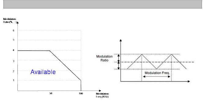
3.Spread Spectrum Rate (SSR) for 50KHz ~ 100kHz Modulation Frequency(FMOD) is calculated by (7 – 0.06*Fmod), where Modulation Frequency (FMOD) unit is KHz.
LVDS Receiver Spread spectrum Clock is defined as below figure
Timing should be set based on clock frequency.
Ver. 0.1 |
7 /43 |
|
|
PDF created with pdfFactory Pro trial version www.pdffactory.com
LC420DUJ
Product Specification
Please pay attention to the followings when you set Spread Spectrum Rate(SSR) and Modulation Frequency(FMOD)
1.Please set proper Spread Spectrum Rate(SSR) and Modulation Frequency (FMOD) of TV system LVDS output.
2.Please check FOS after you set Spread Spectrum Rate(SSR) and Modulation Frequency(FMOD) to avoid abnormal display. Especially, harmonic noise can appear when you use Spread Spectrum under FMOD 30 KHz.
Ver. 0.1 |
8 /43 |
|
|
PDF created with pdfFactory Pro trial version www.pdffactory.com

LC420DUJ
Product Specification
3-4. LVDS Signal Specification
3-4-1. LVDS Input Signal Timing Diagram
0.7VDD
DE, Data
0.3VDD
|
tCLK |
0.5 VDD |
|
|
|
DCLK |
|
|
First data |
|
Invalid data |
Second data |
|
Invalid data |
|
DE(Data Enable) |
|
|
Valid data |
|
|
Pixel |
0,0 |
Pixel |
2,0 |
|
Valid data |
|
|
Pixel |
1,0 |
Pixel |
3,0 |
tHV
tHP
1 |
1080 |
DE(Data Enable)
Invalid data
Invalid data
tVV
tVP
Ver. 0.1 |
9 /43 |
|
|
PDF created with pdfFactory Pro trial version www.pdffactory.com
LC420DUJ
Product Specification
3-4-2. LVDS Input Signal Characteristics
1) DC Specification
LVDS |
- |
|
|
|
|
|
|
LVDS |
+ |
|
|
|
|
|
|
|
|
|
|
|
V CM |
V IN _ MAX |
V IN _ MIN |
|
# V CM |
= {(LVDS |
+) + ( |
LVDS |
-)}/2 |
|
|
0V |
|
|
|
|
|
|
|
Description |
Symbol |
Min |
Max |
Unit |
notes |
LVDS Common mode Voltage |
VCM |
1.0 |
1.5 |
V |
- |
LVDS Input Voltage Range |
VIN |
0.7 |
1.8 |
V |
- |
Change in common mode Voltage |
VCM |
- |
250 |
mV |
- |
|
|
|
|
|
|
2) AC Specification
Tclk
LVDS Clock
LVDS Data
(Fclk = 1/Tclk )
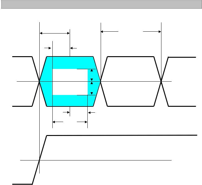
tSKEW tSKEW
Tclk
LVDS 1’st Clock
LVDS 2nd Clock
tSKEW_min tSKEW_max
Description |
Symbol |
Min |
Max |
Unit |
notes |
|
LVDS Differential Voltage |
VTH |
100 |
600 |
mV |
Tested with Differential Probe |
|
VTL |
-600 |
-100 |
mV |
2 |
||
|
||||||
LVDS Clock to Data Skew |
tSKEW |
- |
|(0.25*Tclk)/7| |
ps |
- |
|
Effective time of LVDS |
teff |
|±360| |
- |
ps |
- |
|
LVDS Clock to Clock Skew (Even to Odd) |
tSKEW_EO |
- |
|1/7* Tclk| |
ps |
- |
notes 1. All Input levels of LVDS signals are based on the EIA 644 Standard.
2.If tRF isn’t enough, teff should be meet the range.
3.LVDS Differential Voltage is defined within teff
Ver. 0.1 |
10 /43 |
|
|
PDF created with pdfFactory Pro trial version www.pdffactory.com
LC420DUJ
Product Specification
0.5tui |
tui |
LVDS Data |
|
360ps |
|
|
VTH |
0V |
|
(Differential) |
VTL |
|
360ps |
teff |
|
LVDS CLK |
tui : Unit Interval |
0V |
|
(Differential) |
|
* This accumulated waveform is tested with differential probe
Ver. 0.1 |
11 /43 |
|
|
PDF created with pdfFactory Pro trial version www.pdffactory.com
 Loading...