


LC420EUF
Product Specification
SPECIFICATION
FOR
APPROVAL
() Preliminary Specification
( ●) Final Specification
Title |
42.0” WUXGA TFT LCD |
|
|
BUYER |
TP VISION |
|
|
MODEL |
|
|
|
SUPPLIER |
LG Display Co., Ltd. |
|
|
*MODEL |
LC420EUF |
|
|
SUFFIX |
PEF1 (RoHS Verified) |
|
|
*When you obtain standard approval,
please use the above model name without suffix
APPROVED BY
SIGNATURE
DATE
/
/
/
Please return 1 copy for your confirmation with your signature and comments.
Ver. 1.0 |
1 /43 |
|
|
|
|
LC420EUF |
|
|
|
|
Product Specification |
|
|
CONTENTS |
|
|
|
|
Number |
ITEM |
Page |
|
|
|
|
COVER |
1 |
|
CONTENTS |
2 |
|
RECORD OF REVISIONS |
3 |
1 |
GENERAL DESCRIPTION |
4 |
2 |
ABSOLUTE MAXIMUM RATINGS |
5 |
3 |
ELECTRICAL SPECIFICATIONS |
6 |
3-1 |
ELECTRICAL CHARACTERISTICS |
6 |
3-2 |
INTERFACE CONNECTIONS |
8 |
3-3 |
SIGNAL TIMING SPECIFICATIONS |
11 |
3-4 |
LVDS SIGNAL SPECIFICATIONS |
12 |
3-5 |
COLOR DATA REFERENCE |
15 |
3-6 |
POWER SEQUENCE |
16 |
4 |
OPTICAL SPECIFICATIONS |
17 |
5 |
MECHANICAL CHARACTERISTICS |
23 |
6 |
RELIABILITY |
26 |
7 |
INTERNATIONAL STANDARDS |
27 |
7-1 |
SAFETY |
27 |
7-2 |
EMC |
27 |
7-3 |
ENVIRONMENT |
27 |
8 |
PACKING |
28 |
8-1 |
INFORMATION OF LCM LABEL |
28 |
8-2 |
PACKING FORM |
28 |
9 |
PRECAUTIONS |
29 |
9-1 |
MOUNTING PRECAUTIONS |
29 |
9-2 |
OPERATING PRECAUTIONS |
29 |
9-3 |
ELECTROSTATIC DISCHARGE CONTROL |
30 |
9-4 |
PRECAUTIONS FOR STRONG LIGHT EXPOSURE |
30 |
9-5 |
STORAGE |
30 |
9-6 |
OPERAGING CONDITION GUIDE |
30 |
|
|
|
|
|
|
Ver. 1.0 |
|
2 /43 |
|
|
|
LC420EUF
|
|
|
Product Specification |
|
|
|
RECORD OF REVISIONS |
||
|
|
|
|
|
Revision No. |
Revision Date |
Page |
|
Description |
|
|
|
|
|
0.1 |
Feb. 02, 2012 |
- |
|
Preliminary Specification (First Draft) |
|
|
|
|
|
0.2 |
Mar. 07, 2012 |
28 |
|
Updated LCM quatities in one pallet.(17 16) |
0.3 |
Apr. 03, 2012 |
- |
|
Spec. updated |
0.4 |
Apr. 24, 2012 |
24,25 |
|
Updated LCM mechanical drawing. |
0.5 |
MAY. 03, 2012 |
25 |
|
Updated Torque spec |
1.0 |
MAY. 09, 2012 |
- |
|
Final Specification |
|
|
|
|
|
|
|
|
|
|
|
|
|
|
|
|
|
|
|
|
|
|
|
|
|
|
|
|
|
|
|
|
|
|
|
|
|
|
|
|
|
|
|
|
|
|
|
|
|
|
|
|
|
|
|
|
|
|
|
|
|
|
|
|
|
|
|
|
|
|
|
|
|
|
|
|
|
|
|
|
|
|
|
|
|
|
|
|
|
|
|
|
|
|
|
|
|
|
|
|
|
|
|
|
|
|
|
|
|
|
|
|
|
|
|
Ver. 1.0 |
3 /43 |
|
|
LC420EUF
Product Specification
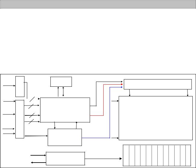
1. General Description
The LC420EUF is a Color Active Matrix Liquid Crystal Display with an integral Light Emitting Diode (LED) backlight system. The matrix employs a-Si Thin Film Transistor as the active element. It is a transmissive display type which is operating in the normally black mode. It has a 42.02 inch diagonally measured active display area with WUXGA resolution (1080 vertical by 1920 horizontal pixel array). Each pixel is divided into Red, Green and Blue sub-pixels or dots which are arrayed in vertical stripes. Gray scale or the luminance of the sub-pixel color is determined with a 10-bit gray scale signal for each dot. Therefore, it can present a palette of more than 1.06Bilion colors.
It has been designed to apply the 10-bit 4-port LVDS interface.
It is intended to support LCD TV, PCTV where high brightness, super wide viewing angle, high color gamut, high color depth and fast response time are important.
|
CN2 |
|
EEPROM |
EPI (RGB) |
|
||
LVDS |
|
|
|
Source Driver Circuit |
|||
(41pin) |
|
|
|
|
|
||
2Port |
|
|
|
|
|
|
|
|
|
LVDS 3,4 |
SCL |
SDA |
|
S1 |
S1920 |
LVDS |
|
|
|
|
|
G1 |
|
2Port |
|
LVDS 1,2 |
Timing Controller |
|
|
|
|
LVDS |
|
|
|
|
|
||
|
Option |
LVDS Rx + DGA + ODC |
|
|
TFT - LCD Panel |
||
Select |
|
Control |
|
||||
|
signal |
|
Integrated |
|
|||
|
|
|
|
Signals |
|
(1920 × RGB × 1080 pixels) |
|
|
|
I2C |
|
|
|
||
|
CN1 |
|
|
|
|
||
Bit |
|
|
|
|
|
[Gate In Panel] |
|
(51pin) |
|
|
|
|
|
||
Select |
|
|
|
|
|
|
|
+12.0V |
|
|
|
|
Power Signals |
|
|
|
|
|
Power Circuit |
G1080 |
|
||
|
|
|
|
Block |
|
|
|
LED Anode |
|
|
|
|
|
Backlight Assembly |
|
|
CN201 (8pin) |
|
|
H : 12 Block |
|||
|
|
|
CN202 (8pin) |
|
|
||
LED Cathode |
|
|
|
||||
|
|
|
|
|
|||
General Features
Active Screen Size |
42.02 Inches(1067.31mm) diagonal |
Outline Dimension |
950.0(H) X 554.6(V) X 9.4(B)/16.9(D) |
Pixel Pitch |
0.4845 mm x 0.4845 mm |
Pixel Format |
1920 horiz. by 1080 vert. Pixels, RGB stripe arrangement |
Color Depth |
10bit(D), 1.06Billon colors |
Luminance, White |
400 cd/m2 (Center 1point ,Typ.) |
Viewing Angle (CR>10) |
Viewing angle free ( R/L 178 (Min.), U/D 178 (Min.)) |
Power Consumption |
Total 60.6W (Typ.) [Logic=8.4W, LED Backlight=52.2W (IF_cathode=85mA)] |
Weight |
8.6 Kg (Typ.) |
Display Mode |
Transmissive mode, Normally black |
Surface Treatment |
Hard coating(2H),Anti-glare treatment of the front polarizer (Haze 1%) |
|
|
Ver. 1.0 |
4 /43 |
|
|
LC420EUF
Product Specification
2. Absolute Maximum Ratings
The following items are maximum values which, if exceeded, may cause faulty operation or permanent damage to the LCD module.
Table 1. ABSOLUTE MAXIMUM RATINGS
Parameter |
Symbol |
|
Value |
Unit |
Note |
|||
|
|
|
||||||
Min |
|
Max |
||||||
|
|
|
|
|
|
|
||
Power Input Voltage |
|
LCD Circuit |
VLCD |
-0.3 |
|
+14.0 |
VDC |
|
|
|
|
|
|
|
|
|
1 |
LED Input Voltage |
|
Forward Voltage |
VF |
- |
|
+71.2 |
VDC |
|
|
|
|
||||||
|
|
|
|
|
|
|
|
|
T-Con Option Selection Voltage |
VLOGIC |
-0.3 |
|
+4.0 |
VDC |
|
||
Operating Temperature |
|
TOP |
0 |
|
+50 |
°C |
|
|
Storage Temperature |
|
TST |
-20 |
|
+60 |
°C |
2,3 |
|
|
|
|
||||||
Panel Front Temperature |
|
TSUR |
- |
|
+68 |
°C |
4 |
|
Operating Ambient Humidity |
HOP |
10 |
|
90 |
%RH |
|
||
Storage Humidity |
|
HST |
10 |
|
90 |
%RH |
2,3 |
|
|
|
|
||||||
|
|
|
|
|
|
|
|
|
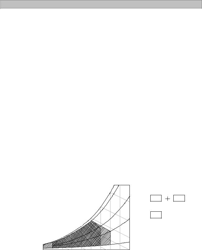
Note1. Ambient temperature condition (Ta = 25 ± 2 °C )
2.Temperature and relative humidity range are shown in the figure below. Wet bulb temperature should be Max 39°C, and no condensation of water.
3.Gravity mura can be guaranteed below 40°C condition.
4.The maximum operating temperatures is based on the test condition that the surface temperature
of display area is less than or equal to 68°C with LCD module alone in a temperature controlled chamber. Thermal management should be considered in final product design to prevent the surface temperature of display area from being over 68 . The range of operating temperature may be degraded in case of improper thermal management in final product design.
|
|
|
|
|
|
|
|
90% |
|
|
|
|
|
|
|
|
|
60 |
|
|
|
|
|
|
|
|
|
|
|
|
60% |
|
|
|
|
|
|
|
50 |
|
|
[(%)RH] |
Storage |
|
Wet Bulb |
|
|
|
|
|
|
|
||
|
|
|
|
|
|
|
|
|
||
|
Temperature [°C] |
|
40 |
|
|
|
|
|
||
|
|
|
|
|
|
|
|
Humidity |
|
|
|
|
|
|
|
|
|
|
|
40% |
Operation |
|
|
|
|
30 |
|
|
|
|
|
|
|
|
|
|
|
|
|
|
|
|
|
|
|
|
20 |
|
|
|
|
|
|
|
|
|
10 |
|
|
|
|
|
|
|
|
|
0 |
|
|
|
|
|
|
|
10% |
|
|
|
|
|
|
|
|
|
|
|
|
-20 |
0 |
10 |
20 |
30 |
40 |
50 |
60 |
70 |
80 |
|
|
|
Dry Bulb Temperature [°C] |
|
|
|
|
||||
Ver. 1.0 |
5 /43 |
|
|
LC420EUF
Product Specification
3. Electrical Specifications
3-1. Electrical Characteristics
It requires two power inputs. One is employed to power for the LCD circuit. The other Is used for the LED backlight.
Table 2. ELECTRICAL CHARACTERISTICS
|
|
|
Value |
|
|
|
|
Parameter |
Symbol |
|
|
|
Unit |
Note |
|
Min |
Typ |
Max |
|||||
|
|
|
|
||||
|
|
|
|
|
|
|
|
Circuit : |
|
|
|
|
|
|
|
|
|
|
|
|
|
|
|
Power Input Voltage |
VLCD |
10.8 |
12.0 |
13.2 |
VDC |
|
|
|
|
|
|
|
|
|
|
|
|
- |
700 |
910 |
mA |
1 |
|
Power Input Current |
ILCD |
|
|
|
|
|
|
- |
1010 |
1313 |
mA |
2 |
|||
|
|
||||||
|
|
|
|
|
|
|
|
Power Consumption |
PLCD |
- |
8.4 |
10.9 |
Watt |
1 |
|
|
|
|
|
|
|
|
|
Rush current |
IRUSH |
- |
- |
5.0 |
A |
3 |
|
|
|
|
|
|
|
|
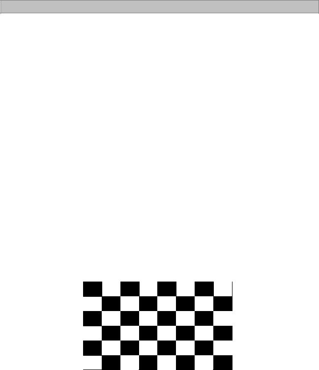
Note 1. The specified current and power consumption are under the VLCD=12.0V, Ta=25 ± 2°C, fV=120Hz condition, and mosaic pattern(8 x 6) is displayed and fV is the frame frequency.
2.The current is specified at the maximum current pattern.
3.The duration of rush current is about 2ms and rising time of power input is 0.5ms (min.).
4.Ripple voltage level is recommended under ±5% of typical voltage
White : 1023 Gray
Black : 0 Gray
Mosaic Pattern(8 x 6)
Ver. 1.0 |
6 /43 |
|
|

|
|
|
|
|
|
|
|
LC420EUF |
|
|
|
|
|
|
|
|
|
|
|
|
|
|
Product Specification |
|
|
|
|
||
Table 3. ELECTRICAL CHARACTERISTICS (Continue) |
|
|
|
|
|
||||
|
|
|
|
|
|
|
|
|
|
Parameter |
Symbol |
|
Values |
|
Unit |
Note |
|
||
|
|
|
|
||||||
|
|
|
|
Min |
Typ |
Max |
|
|
|
Backlight Assembly : |
|
|
|
|
|
|
|
||
|
|
|
|
|
|
|
|
|
|
Forward Current |
|
Anode |
IF (anode) |
|
510 |
|
mAdc |
±5% |
|
(one array) |
|
Cathode |
IF (cathode) |
80.8 |
85 |
89.3 |
mAdc |
2, 3 |
|
Forward Voltage |
|
VF |
47.2 |
51.2 |
55.2 |
Vdc |
4 |
|
|
Forward Voltage Variation |
VF |
|
|
1.7 |
Vdc |
5 |
|
||
Power Consumption |
|
PBL |
|
52.2 |
56.3 |
W |
6 |
|
|
Burst Dimming Duty |
|
On duty |
1 |
|
100 |
% |
|
|
|
Burst Dimming Frequency |
1/T |
|
100/120 |
|
Hz |
8 |
|
||
LED Array : |
|
|
|
|
|
|
|
|
|
|
|
|
|
|
|
|
|
|
|
Life Time |
|
|
30,000 |
50,000 |
|
Hrs |
7 |
|
|
Note :
The design of the LED driver must have specifications for the LED array in LCD Assembly. The electrical characteristics of LED driver are based on Constant Current driving type.
The performance of the LED in LCM, for example life time or brightness, is extremely influenced by the characteristics of the LED Driver. So, all the parameters of an LED driver should be carefully designed. When you design or order the LED driver, please make sure unwanted lighting caused by the mismatch of the LED and the driver (no lighting, flicker, etc) has never been occurred. When you confirm it, the LCD– Assembly should be operated in the same condition as installed in your instrument.
1.Electrical characteristics are based on LED Array specification.
2.Specified values are defined for a Backlight Assembly. (IBL : 2 LED array/LCM)
3.Each LED array has one anode terminal and 6 cathode terminals.
The forward current(IF) of the anode terminal is 510mA and it supplies 85mA into 6 strings, respectively
8 (LED Pakage / 1string)
Anode
° ° °
° ° ° |
Cathode #1 |
° ° ° |
Cathode #2 |
|
6 (LED String / 1 Array) |
° ° ° |
Cathode #6 |
4.The forward voltage(VF) of LED array depends on ambient temperature (Appendix-V)
5.VF means Max VF-Min VF in one Backlight. So VF variation in a Backlight isn’t over Max. 1.7V
6.Maximum level of power consumption is measured at initial turn on.
Typical level of power consumption is measured after 1hrs aging at 25 ± 2°C.
7.The life time(MTTF) is determined as the time at which brightness of the LED is 50% compared to that of initial value at the typical LED current on condition of continuous operating at 25 ± 2°C, based on duty 100%.
8.The reference method of burst dimming duty ratio.
It is recommended to use synchronous V-sync frequency to prevent waterfall (Vsync x 1 =Burst Frequency)
.
Ver. 1.0 |
7 /43 |
|
|

LC420EUF
Product Specification
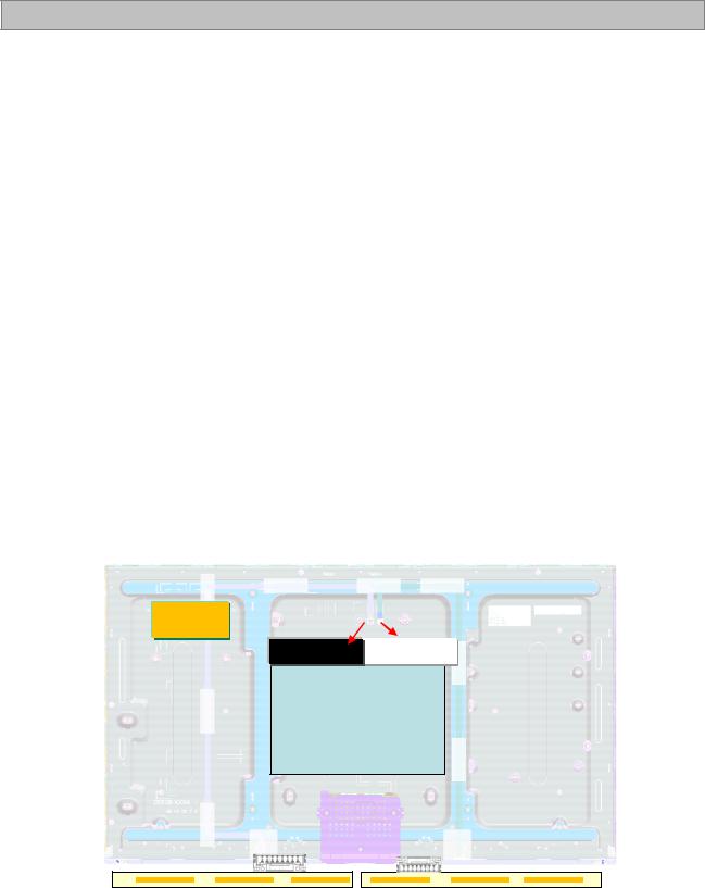
3-2. Interface Connections
This LCD module employs two kinds of interface connection, 51-pin connector and 41-pin connector are used for the module electronics and Two 8-pin connectors are used for the integral backlight system.
3-2-1. LCD Module
- LCD Connector(CN1): FI-RE51S-HF(manufactured by JAE) or GT05P-51S-H38(manufactured by LSM) or IS050-C51B-C39(manufactured by UJU)
- Mating Connector : FI-R51HL(JAE) or compatible
Table 4-1. MODULE CONNECTOR(CN1) PIN CONFIGURATION
No |
|
Symbol |
Description |
|
No |
Symbol |
Description |
|
|
|
|
|
|
|
|
1 |
|
PCID_EN |
‘H’ : PCID Enable, ‘L’ or NC: PCID |
|
27 |
Bit Select |
‘H’ or NC= 10bit(D) , ‘L’ = 8bit |
|
Disable (3D Mode only) |
|
|||||
|
|
|
|
|
|
|
|
|
|
|
|
|
|
|
|
2 |
|
NC |
No Connection (Note 4) |
|
28 |
R2AN |
SECOND LVDS Receiver Signal (A-) |
3 |
|
NC |
No Connection (Note 4) |
|
29 |
R2AP |
SECOND LVDS Receiver Signal (A+) |
4 |
|
NC |
No Connection (Note 4) |
|
30 |
R2BN |
SECOND LVDS Receiver Signal (B-) |
5 |
|
NC |
No Connection (Note 4) |
|
31 |
R2BP |
SECOND LVDS Receiver Signal (B+) |
6 |
|
NC |
No Connection (Note 4) |
|
32 |
R2CN |
SECOND LVDS Receiver Signal (C-) |
7 |
|
LVDS Select |
‘H’ =JEIDA , ‘L’ or NC = VESA |
|
33 |
R2CP |
SECOND LVDS Receiver Signal (C+) |
8 |
|
NC |
No Connection (Note 4) |
|
34 |
GND |
Ground |
9 |
|
NC |
No Connection (Note 4) |
|
35 |
R2CLKN |
SECOND LVDS Receiver Clock Signal(-) |
10 |
|
NC |
No Connection (Note 4) |
|
36 |
R2CLKP |
SECOND LVDS Receiver Clock Signal(+) |
11 |
|
GND |
Ground |
|
37 |
GND |
Ground |
12 |
|
R1AN |
FIRST LVDS Receiver Signal (A-) |
|
38 |
R2DN |
SECOND LVDS Receiver Signal (D-) |
13 |
|
R1AP |
FIRST LVDS Receiver Signal (A+) |
|
39 |
R2DP |
SECOND LVDS Receiver Signal (D+) |
14 |
|
R1BN |
FIRST LVDS Receiver Signal (B-) |
|
40 |
R2EN |
SECOND LVDS Receiver Signal (E-) |
15 |
|
R1BP |
FIRST LVDS Receiver Signal (B+) |
|
41 |
R2EP |
SECOND LVDS Receiver Signal (E+) |
16 |
|
R1CN |
FIRST LVDS Receiver Signal (C-) |
|
42 |
NC or GND |
No Connection or Ground |
17 |
|
R1CP |
FIRST LVDS Receiver Signal (C+) |
|
43 |
NC or GND |
No Connection or Ground |
18 |
|
GND |
Ground |
|
44 |
GND |
Ground (Note 6) |
19 |
|
R1CLKN |
FIRST LVDS Receiver Clock Signal(-) |
|
45 |
GND |
Ground |
20 |
|
R1CLKP |
FIRST LVDS Receiver Clock Signal(+) |
|
46 |
GND |
Ground |
21 |
|
GND |
Ground |
|
47 |
NC |
No connection |
22 |
|
R1DN |
FIRST LVDS Receiver Signal (D-) |
|
48 |
VLCD |
Power Supply +12.0V |
23 |
|
R1DP |
FIRST LVDS Receiver Signal (D+) |
|
49 |
VLCD |
Power Supply +12.0V |
24 |
|
R1EN |
FIRST LVDS Receiver Signal (E-) |
|
50 |
VLCD |
Power Supply +12.0V |
25 |
|
R1EP |
FIRST LVDS Receiver Signal (E+) |
|
51 |
VLCD |
Power Supply +12.0V |
26 |
|
NC or GND |
No Connection or Ground |
|
- |
- |
- |
Note |
1. All GND (ground) pins should be connected together to the LCD module’s metal frame. |
||||||
2.All VLCD (power input) pins should be connected together.
3.All Input levels of LVDS signals are based on the EIA 644 Standard.
4.#2~#6 & #8~#10 NC (No Connection): These pins are used only for LGD (Do not connect)
5.LVDS pin (pin No. #24,25,40,41) are used for 10Bit(D) of the LCD module. If used for 8Bit(R), these pins are no connection.
6.Specific pin No. #44 is used for “No signal detection” of system signal interface.
It should be GND for NSB (No Signal Black) while the system interface signal is not. If this pin is “H”, LCD Module displays AGP (Auto Generation Pattern).
Ver. 1.0 |
8 /43 |
|
|
LC420EUF
Product Specification
- LCD Connector(CN2): FI-RE41S-HF(manufactured by JAE) or GT05P-41S-H38(manufactured by LSM) or IS050-C41B-C39(manufactured by UJU)
- Mating Connector : FI-RE41HL(JAE) or compatible
Table 4-2. MODULE CONNECTOR(CN2) PIN CONFIGURATION
No |
Symbol |
Description |
|
No |
Symbol |
Description |
1 |
NC |
No connection |
|
22 |
RE3N |
THIRD LVDS Receiver Signal (E-) |
2 |
NC |
No connection |
|
23 |
RE3P |
THIRD LVDS Receiver Signal (E+) |
3 |
NC |
No connection |
|
24 |
GND |
Ground |
4 |
NC |
No connection |
|
25 |
GND |
Ground |
5 |
NC |
No connection |
|
26 |
RA4N |
FORTH LVDS Receiver Signal (A-) |
6 |
NC |
No connection |
|
27 |
RA4P |
FORTH LVDS Receiver Signal (A+) |
7 |
NC |
No connection |
|
28 |
RB4N |
FORTH LVDS Receiver Signal (B-) |
8 |
NC |
No connection |
|
29 |
RB4P |
FORTH LVDS Receiver Signal (B+) |
9 |
GND |
Ground |
|
30 |
RC4N |
FORTH LVDS Receiver Signal (C-) |
10 |
RA3N |
THIRD LVDS Receiver Signal (A-) |
|
31 |
RC4P |
FORTH LVDS Receiver Signal (C+) |
11 |
RA3P |
THIRD LVDS Receiver Signal (A+) |
|
32 |
GND |
Ground |
12 |
RB3N |
THIRD LVDS Receiver Signal (B-) |
|
33 |
RCLK4N |
FORTH LVDS Receiver Clock Signal(-) |
13 |
RB3P |
THIRD LVDS Receiver Signal (B+) |
|
34 |
RCLK4P |
FORTH LVDS Receiver Clock Signal(+) |
14 |
RC3N |
THIRD LVDS Receiver Signal (C-) |
|
35 |
GND |
Ground |
15 |
RC3P |
THIRD LVDS Receiver Signal (C+) |
|
36 |
RD4N |
FORTH LVDS Receiver Signal (D-) |
16 |
GND |
Ground |
|
37 |
RD4P |
FORTH LVDS Receiver Signal (D+) |
17 |
RCLK3N |
THIRD LVDS Receiver Clock Signal(-) |
|
38 |
RE4N |
FORTH LVDS Receiver Signal (E-) |
18 |
RCLK3P |
THIRD LVDS Receiver Clock Signal(+) |
|
39 |
RE4P |
FORTH LVDS Receiver Signal (E+) |
19 |
GND |
Ground |
|
40 |
GND |
Ground |
20 |
RD3N |
THIRD LVDS Receiver Signal (D-) |
|
41 |
GND |
Ground |
21 |
RD3P |
THIRD LVDS Receiver Signal (D+) |
|
- |
|
|
Note : 1. All GND (ground) pins should be connected together to the LCD module’s metal frame.
2.LVDS pin (pin No. #22,23,38,39) are used for 10Bit(D) of the LCD module. If used for 8Bit(R), these pins are no connection.
|
|
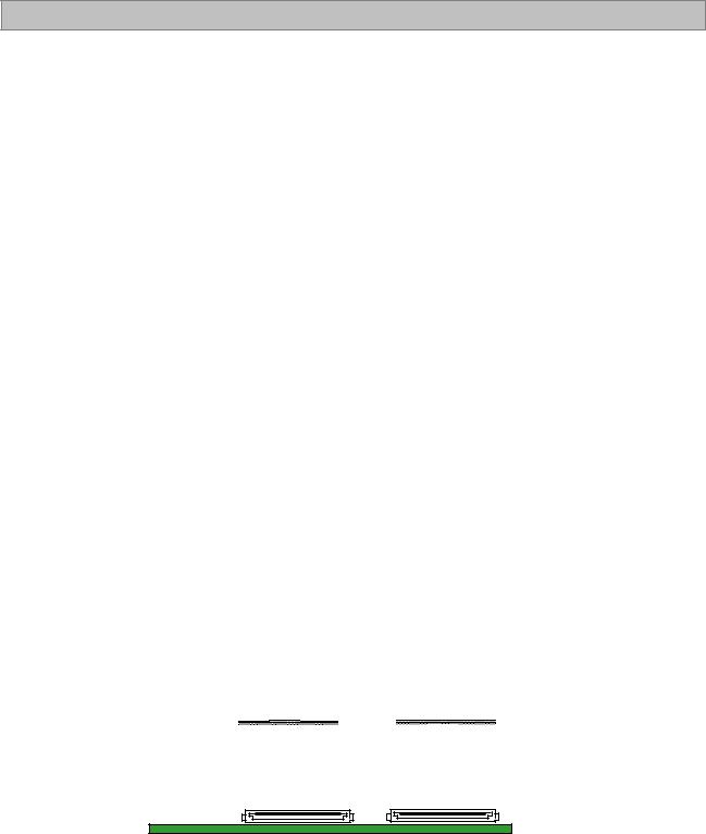
#1 CN1 |
#51 |
|
#1 CN2 #41 |
||
|
|
|
|
|
|
|
|
|
|
|
|
|
|
|
|
|
|
|
|
|
|
|
|
#1 CN1 #51 #1 CN2 #41
Rear view of LCM
Ver. 1.0 |
9 /43 |
|
|
LC420EUF
Product Specification
3-2-2. Backlight Module
[ CN201 ] |
[ CN202 ] |
|
1)LED Array ass`y Connector (Plug)
:HS100-L08N-N62, (black color, manufactured by UJU)
2)Mating Connector (Receptacle)
:IS100-L08T-C46 (black color, manufactured by UJU)
1)LED Array ass`y Connector (Plug)
:HS100-L08N-N62-A (natural color, manufactured by UJU)
2)Mating Connector (Receptacle)
:IS100-L08T-C46-A (natural color, manufactured by UJU)
Table 5. BACKLIGHT CONNECTOR PIN CONFIGURATION(CN201,CN202)
No |
Symbol(CN201) |
Description |
Note |
1 |
L1 Cathode |
LED Output Current |
|
2 |
L2 Cathode |
LED Output Current |
|
3 |
L3 Cathode |
LED Output Current |
|
4 |
L4 Cathode |
LED Output Current |
|
5 |
L5 Cathode |
LED Output Current |
|
6 |
L6 Cathode |
LED Output Current |
|
7 |
N.C |
Open |
|
8 |
Anode_L |
LED Input Current for |
|
L1~L6 |
|
||
|
|
|
|
|
|
|
|
No |
Symbol(CN202) |
Description |
Note |
1 |
Anode_R |
LED Input Current for |
|
R1~R6 |
|
||
|
|
|
|
2 |
N.C |
Open |
|
3 |
R6 Cathode |
LED Output Current |
|
4 |
R5 Cathode |
LED Output Current |
|
5 |
R4 Cathode |
LED Output Current |
|
6 |
R3 Cathode |
LED Output Current |
|
7 |
R2 Cathode |
LED Output Current |
|
8 |
R1 Cathode |
LED Output Current |
|
|
|
|
|
Rear
87654321 87654321
CN201(B) CN202(W)
Buyer LPB
L1 |
L2 |
L3 |
R1 |
R2 |
R3 |
Ver. 1.0 |
10 /43 |
|
|
LC420EUF
Product Specification
3-3. Signal Timing Specifications
Table 6 shows the signal timing required at the input of the LVDS transmitter. All of the interface signal timings should be satisfied with the following specification for normal operation.
Table 6. TIMING TABLE (DE Only Mode)
ITEM |
|
Symbol |
Min |
Typ |
Max |
Unit |
Note |
|
|
|
|
|
|
|
|
|
|
|
|
Display |
tHV |
480 |
480 |
480 |
tCLK |
1920 / 4 |
|
|
Period |
||||||
|
|
|
|
|
|
|
|
|
Horizontal |
|
|
|
|
|
|
|
|
|
Blank |
tHB |
40 |
70 |
200 |
tCLK |
1 |
|
|
|
|||||||
|
|
|
|
|
|
|
|
|
|
|
Total |
tHP |
520 |
550 |
680 |
tCLK |
|
|
|
|
|
|
|
|
|
|
|
|
Display |
tVV |
1080 |
1080 |
1080 |
Lines |
|
|
|
Period |
|
|||||
|
|
|
|
|
|
|
|
|
|
|
|
|
|
|
|
|
|
Vertical |
|
Blank |
tVB |
20 |
45 |
86 |
Lines |
1 |
|
(228) |
(270) |
(300) |
|||||
|
|
|
|
|
|
|||
|
|
|
|
|
|
|
|
|
|
|
Total |
tVP |
1100 |
1125 |
1166 |
Lines |
|
|
|
(1308) |
(1350) |
(1380) |
|
|||
|
|
|
|
|
|
|||
|
|
|
|
|
|
|
|
|
|
|
|
|
|
|
|
|
|
ITEM |
|
Symbol |
Min |
Typ |
Max |
Unit |
Note |
|
|
|
|
|
|
|
|
|
|
|
|
DCLK |
fCLK |
66.97 |
74.25 |
78.00 |
MHz |
|
|
|
|
|
|
|
|
|
|
|
|
Horizontal |
fH |
121.8 |
135 |
140 |
KHz |
2 |
Frequency |
|
|
|
|
|
|
|
|
|
|
|
|
|
|
|
2 |
|
|
|
|
|
108 |
120 |
122 |
|
|
|
|
Vertical |
fV |
Hz |
NTSC |
|||
|
|
(95) |
(100) |
(104) |
||||
|
|
|
|
|
(PAL) |
|||
|
|
|
|
|
|
|
|
|
|
|
|
|
|
|
|
|
|
Note: 1. The input of HSYNC & VSYNC signal does not have an effect on normal operation (DE Only Mode). If you use spread spectrum of EMI, add some additional clock to minimum value for clock margin.
2.The performance of the electro-optical characteristics may be influenced by variance of the vertical refresh rate and the horizontal frequency
Timing should be set based on clock frequency.
Ver. 1.0 |
11 /43 |
|
|
LC420EUF
Product Specification
3-4. LVDS Signal Specification
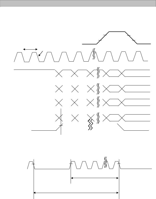
3-4-1. LVDS Input Signal Timing Diagram
0.7VDD
DE, Data
0.3VDD
DCLK |
|
|
tCLK |
|
0.5 VDD |
|
|
|
|
||||
|
|
|
|
|
||
|
|
|
|
|
|
|
|
|
|
|
|
|
|
|
|
|
|
|
|
|
|
|
|
|
|
|
|
Valid data
First data |
Invalid data |
Pixel |
0 |
|
Pixel |
4 |
|
|
|
|
|
|
|||||||||
|
|
|
|
|
|
|
|
|
|
|
|
|
|
|
|
|
|
|
|
|
|
|
|
|
|
|
|
|
|
Valid data |
|
|
|
|
|
|
|
||||||
|
|
|
|
|
|
|
|
|
|
|
|
|
|
|
|
|
|
|
|
||
Second data |
Invalid data |
Pixel |
1 |
|
Pixel |
5 |
|
|
|
|
|
|
|||||||||
|
|
|
|
|
|
|
|
|
|
|
|
|
|
|
|
|
|
|
|
||
|
|
|
|
|
|
|
|
Valid data |
|
|
|
|
|
|
|
||||||
|
|
|
|
|
|
|
|
|
|
|
|
|
|
|
|
||||||
Third data |
Invalid data |
Pixel |
2 |
|
Pixel |
6 |
|
|
|
|
|
|
|||||||||
|
|
|
|
|
|
|
|
|
|
|
|
|
|
|
|
|
|
|
|||
|
|
|
|
|
|
|
|
Valid data |
|
|
|
|
|
|
|
||||||
|
|
|
|
|
|
|
|
|
|
|
|
|
|
|
|
||||||
Forth data |
Invalid data |
Pixel |
3 |
|
Pixel 7 |
|
|
|
|
|
|
||||||||||
|
|
|
|
|
|
|
|
|
|
|
|
|
|
|
|
|
|
|
|
|
|
|
|
|
|
|
|
|
|
|
|
|
|
|
|
|
|
|
|
|
|
|
|
DE(Data Enable)
Invalid data
Invalid data
Invalid data
Invalid data
*tHB = tHFP + tWH +tHBP
* tVB = tVFP + tWV +tVBP
1 |
1080 |
DE(Data Enable)
tVV
tVP
Ver. 1.0 |
12 /43 |
|
|

LC420EUF
Product Specification
3-4-2. LVDS Input Signal Characteristics
1) DC Specification
LVDS |
- |
|
|
|
|
|
|
LVDS |
+ |
|
|
|
|
|
|
|
|
|
|
|
V CM |
V IN _ MAX |
V IN _ MIN |
|
# V CM |
= {(LVDS |
+) + ( |
LVDS |
-)}/2 |
|
|
0V |
|
|
|
|
|
|
|
Description |
Symbol |
Min |
Max |
Unit |
Note |
|
|
|
|
|
|
LVDS Common mode Voltage |
VCM |
1.0 |
1.5 |
V |
- |
LVDS Input Voltage Range |
VIN |
0.7 |
1.8 |
V |
- |
Change in common mode Voltage |
VCM |
- |
250 |
mV |
- |
|
|
|
|
|
|
2) AC Specification
|
|
|
|
Tclk |
LVDS Clock |
|
|
|
|
|
|
|
A |
|
LVDS Data |
|
|
|
|
|
|
tSKEW |
(Fclk |
= 1/Tclk ) |
|
|
tSKEW |
A |
|
|
|
|
|
|
|
|
|
Tclk |
|
LVDS 1’st Clock |
|
|
|
80% |
|
|
|
|
|
LVDS 2nd / 3rd / 4th |
Clock |
|
|
|
|
|
|
|
20% |
|
|
|
|
tRF |
|
tSKEW_min |
tSKEW_max |
|
|
Description |
Symbol |
Min |
Max |
Unit |
Note |
|
LVDS Differential Voltage |
VTH |
100 |
600 |
mV |
Tested with Differential Probe |
|
VTL |
-600 |
-100 |
mV |
3 |
||
|
||||||
LVDS Clock to Data Skew |
tSKEW |
- |
|(0.2*Tclk)/7| |
ps |
- |
|
LVDS Clock/DATA Rising/Falling time |
tRF |
260 |
|(0.3*Tclk)/7| |
ps |
2 |
|
Effective time of LVDS |
teff |
|±360| |
- |
ps |
- |
|
LVDS Clock to Clock Skew (Even to Odd) |
tSKEW_EO |
- |
|1/7* Tclk| |
ps |
- |
Note 1. All Input levels of LVDS signals are based on the EIA 644 Standard.
2.If tRF isn’t enough, teff should be meet the range.
3.LVDS Differential Voltage is defined within teff
Ver. 1.0 |
13 /43 |
|
|
 Loading...