


Global LCD Panel Exchange Center |
www.panelook.com |
LC550EUH
Product Specification
SPECIFICATION
FOR
APPROVAL
( ) |
Preliminary Specification |
|
|
|
|
||
( ) |
Final Specification |
|
|
|
|
||
|
|
|
|
|
|
|
|
|
Title |
|
|
55.0” WUXGA TFT LCD |
|||
|
|
|
|
|
|
|
|
|
|
|
|
|
|
||
|
BUYER |
|
|
LGE |
|
SUPPLIER |
LG Display Co., Ltd. |
|
|
|
|
|
|
*MODEL |
LC550EUH |
|
MODEL |
|
|
|
|
||
|
|
|
|
|
|
SUFFIX |
KEF1 (RoHS Verified) |
|
|
|
|
|
|||
|
|
|
|
|
|
*When you obtain standard approval, |
|
please use the above model name without suffix
APPROVED BY
SIGNATURE


 DATE
DATE
/


 /
/
/
Please return 1 copy for your confirmation with your signature and comments.
APPROVED BY |
SIGNATURE |
|
DATE |
||
|
J. M. Kim / Team Leader
REVIEWED BY
Y. N. Lee / Project Leader
PREPARED BY
Y. S. Y / Engineer
TV Product Development Dept.
LG Display Co., Ltd.
Ver. 0.1 |
0 /43 |
|
|
PDF created with pdfFactory Pro trial version www.pdffactory.com |
www.panelook.com |
One step solution for LCD / PDP / OLED panel application: Datasheet, inventory and accessory! |

Global LCD Panel Exchange Center |
www.panelook.com |
|
|
LC550EUH |
|
Product Specification |
|
|
CONTENTS |
|
|
|
|
Number |
ITEM |
Page |
|
COVER |
1 |
|
CONTENTS |
2 |
|
RECORD OF REVISIONS |
3 |
1 |
GENERAL DESCRIPTION |
4 |
2 |
ABSOLUTE MAXIMUM RATINGS |
5 |
3 |
ELECTRICAL SPECIFICATIONS |
6 |
3-1 |
ELECTRICAL CHARACTERISTICS |
6 |
3-2 |
INTERFACE CONNECTIONS |
8 |
3-3 |
SIGNAL TIMING SPECIFICATIONS |
11 |
3-4 |
SIGNAL TIMING WAVEFORMS |
12 |
3-5 |
COLOR DATA REFERENCE |
15 |
3-6 |
POWER SEQUENCE |
16 |
4 |
OPTICAL SPECIFICATIONS |
18 |
5 |
MECHANICAL CHARACTERISTICS |
24 |
6 |
RELIABILITY |
27 |
7 |
INTERNATIONAL STANDARDS |
28 |
7-1 |
SAFETY |
28 |
7-2 |
EMC |
28 |
7-3 |
Environment |
28 |
8 |
PACKING |
29 |
8-1 |
DESIGNATION OF LOT MARK |
29 |
8-2 |
PACKING FORM |
29 |
9 |
PRECAUTIONS |
30 |
9-1 |
MOUNTING PRECAUTIONS |
30 |
9-2 |
OPERATING PRECAUTIONS |
30 |
9-3 |
ELECTROSTATIC DISCHARGE CONTROL |
31 |
9-4 |
PRECAUTIONS FOR STRONG LIGHT EXPOSURE |
31 |
9-5 |
STORAGE |
31 |
9-6 |
HANDLING PRECAUTIONS FOR PROTECTION FILM |
31 |
9-7 |
OPERAGING CONDITION GUIDE |
31 |
|
|
|
|
|
|
Ver. 0.1 |
|
1 /43 |
|
|
|
PDF created with pdfFactory Pro trial version www.pdffactory.com |
www.panelook.com |
One step solution for LCD / PDP / OLED panel application: Datasheet, inventory and accessory! |

Global LCD Panel Exchange Center |
www.panelook.com |
LC550EUH
Product Specification
RECORD OF REVISIONS
Revision No. |
Revision Date |
Page |
Description |
0.1 |
Sep, 26, 2011 |
- |
Preliminary Specification (First Draft) |
0.2 |
Nov,30,2011 |
- |
Revise spec. |
0.3 |
Dec.08.2011 |
7 |
Revise spec. |
Ver. 0.1 |
|
|
2 /43 |
PDF created with pdfFactory Pro trial version www.pdffactory.com |
www.panelook.com |
One step solution for LCD / PDP / OLED panel application: Datasheet, inventory and accessory! |
Global LCD Panel Exchange Center |
www.panelook.com |
LC550EUH
Product Specification
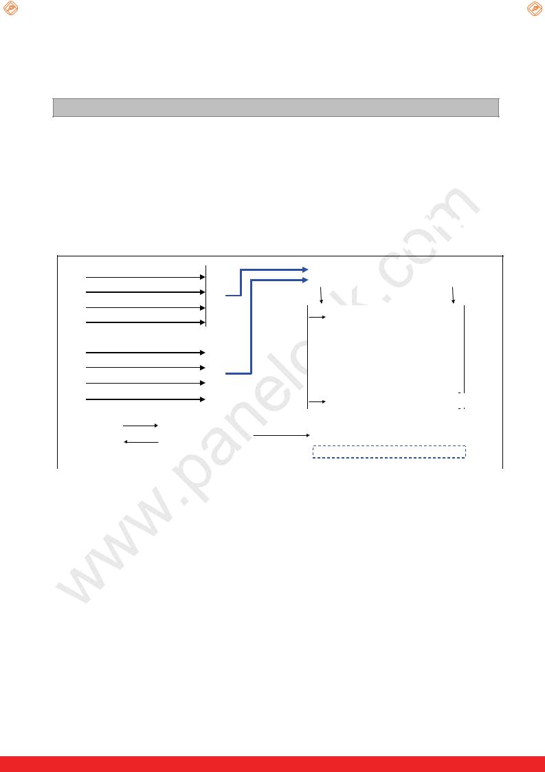
1. General Description
The LC550EUH is a Color Active Matrix Liquid Crystal Display with an integral Light Emitting Diode (LED)
backli ght syst em. T he mat rix employs a-Si Thin Film Transistor as the active |
element. |
It is a transmissive display type which is operating in the normally black mode. It has a 54.64 inch |
diagonally |
measured active display area with WUXGA resolution (1080 vertical by 1920 horizontal pixel array). Each pixel is divided into Red, Green and Blue sub-pixels or dots which are arrayed in vertical stripes. Gray scale or the luminance of the sub-pixel color is determined with a 8-bit gray scale signal for each dot. Therefore, it can present a palette of more than 16.7M(true) colors. 


It is intended to support LCD TV, PCTV where high brightness, super wide viewing angle, high color gamut, high color depth and fast response time are important. 


|
|
|
|
|
|
Power (VCC, Vterm, VDD, HVDD, VGH, VGL) |
|
|
Source Driver Circuit |
|
|
Gate Control Signal |
|
|
|
|
|
CN1 |
|
|
|
|
|
|
S1 |
S1920 |
|
||
|
|
|
|||
Gamma Reference Voltage |
(50pin) |
|
|
|
|
EPI (RGB & Control signal) for Left drive |
|
|
G1 |
|
|
|
|
|
|
|
|
|
|
|
|
|
|
|
Power (VCC, Vterm, VDD, HVDD, VGH, VGL) |
|
|
|
|
|
|
TFT - LCD Panel |
|
||||||
|
|
|
|
|
|
||||||||||
|
|
|
|
|
|
|
|
|
|
|
|
||||
|
Gate Control Signal |
|
|
CN2 |
|
|
|
|
(1920 RGB 1080 pixels) |
|
|||||
|
Gamma Reference Voltage |
|
|
|
|
|
|
[Gate In Panel] |
|
||||||
|
|
(50pin) |
|
|
|
|
|
|
|
|
|
|
|||
|
EPI (RGB & Control Signal) for Right drive |
|
|
|
|
|
G1080 |
|
|
|
|
|
|||
|
|
|
|
|
|
|
|
|
|
|
|
|
|
||
|
LED Anode |
|
|
|
|
|
|
|
|
|
|
|
|
|
|
|
|
|
|
|
|
|
|
|
|
|
|
|
|
|
|
|
|
|
|
|
|
|
|
|
|
|
|
|
|
|
|
|
|
|
|
|
|
|
|
|
|
|
|
|
|
|
|
|
CN1(8Pin), CN2 (8pin) |
|
|
|
|
|
|
|
|
|
|||||
|
|
|
|
|
|
|
|
|
|
|
|||||
|
LED Cathode |
|
|
|
|
|
|
|
|
|
|
|
|
|
|
|
|
|
|
|
|
|
|
|
|
H Local Dimming :12Block |
|
|
|||
|
|
|
|
|
|
|
|
|
|
|
|
|
|
|
|
General Features |
|
|
|
|
|
|
|
|
|
|
|
|
|
||
|
|
|
|
|
|
|
|
|
|
|
|
|
|
||
|
Active Screen Size |
54.64 inches(1387.80mm) diagonal |
|
||||||||||||
|
|
|
|
|
|
|
|
|
|
|
|
|
|
||
|
Outline Dimension |
1228.6(H) X 711.4(V) X 9.3(B) X 20.7(D) |
|
||||||||||||
|
Pixel Pitch |
0.630 mm x 0.630 mm |
|
||||||||||||
|
Pixel Format |
1920 |
horiz. by 1080 vert. Pixels, RGB stripe arrangement |
|
|||||||||||
|
Color Depth |
8-bit, |
16.7 M colors ( 1.06B colors @ 10 bit (D) System Output ) |
|
|||||||||||
|
Drive IC Data Interface |
Source D-IC : 8-bit |
EPI, gamma reference voltage, and control signals |
|
|||||||||||
|
Gate D-IC : Gate In Panel |
|
|||||||||||||
|
|
|
|
||||||||||||
|
Luminance, White |
400 cd/m2 (Center 1point ,Typ.) |
|
||||||||||||
|
Viewing Angle (CR>10) |
Viewing angle free ( R/L 178 (Min.), U/D 178 (Min.)) |
|
||||||||||||
|
Power Consumption |
Total TBD W (Typ.) (Logic=TBD W with T-CON, LED Backlight =98.3W) |
|
||||||||||||
|
Weight |
15.4Kg (Typ.) |
|
|
|
|
|
|
|
|
|||||
|
Display Mode |
Transmissive mode, Normally black |
|
||||||||||||
|
Surface Treatment |
Hard coating(2H), Anti-glare treatment (Haze < 1%), |
|
||||||||||||
|
|
|
|
|
|
|
|
|
|
|
|
|
|
|
|
|
|
|
|
|
|
|
|
|
|
|
|
|
|
|
|
|
Ver. 0.1 |
|
|
|
|
|
3 /43 |
|
|||||||
|
|
|
|
|
|
|
|
|
|
|
|
|
|
|
|
PDF created with pdfFactory Pro trial version www.pdffactory.com |
www.panelook.com |
One step solution for LCD / PDP / OLED panel application: Datasheet, inventory and accessory! |
Global LCD Panel Exchange Center |
www.panelook.com |
LC550EUH
Product Specification
2. Absolute Maximum Ratings
The following items are maximum values which, if exceeded, may cause faulty operation or permanent damage to the LCD module.
Table 1. ABSOLUTE MAXIMUM RATINGS
Parameter |
Symbol |
|
Value |
Unit |
Note |
|
Min |
Max |
|||||
|
|
|
|
|||
Logic & EPI Power Voltage |
VCC |
-0.5 |
+2.2 |
VDC |
|
|
Gate High Voltage |
VGH |
+18.0 |
+30.0 |
VDC |
|
|
Gate Low Voltage |
VGL |
-8.0 |
-4.0 |
VDC |
|
|
Source D-IC Analog Voltage |
VDD |
-0.3 |
+18.0 |
VDC |
1 |
|
Gamma Ref. Voltage (Upper) |
VGMH |
½VDD-0.5 |
VDD+0.5 |
VDC |
|
|
Gamma Ref. Voltage (Low) |
VGML |
-0.3 |
½ VDD+0.5 |
VDC |
|
|
LED Input Voltage |
VF |
- |
+95.0 |
VDC |
|
|
Panel Front Temperature |
TSUR |
- |
+68 |
C |
4 |
|
Operating Temperature |
TOP |
0 |
+50 |
C |
|
|
Storage Temperature |
TST |
-20 |
+60 |
C |
2,3 |
|
Operating Ambient Humidity |
HOP |
10 |
90 |
%RH |
||
|
||||||
Storage Humidity |
HST |
10 |
90 |
%RH |
|
|
Note 1. Ambient temperature condition (Ta = 25 ± 2 C ) |
|
|
|
|
||
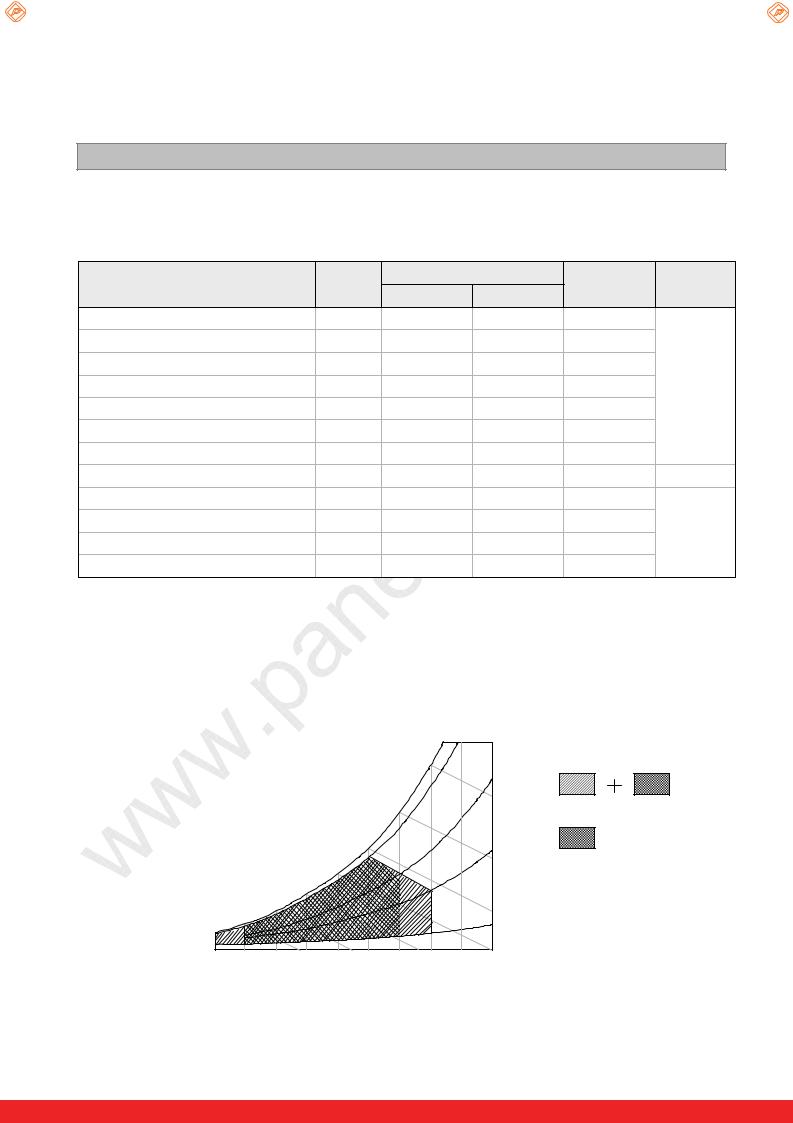
2.Temperature and relative humidity range are shown in the figure below. Wet bulb temperature should be Max 39 C, and no condensation of water.
3.Gravity mura can be guaranteed below 40 C condition.
4.The maximum operating temperatures is based on the test condition that the surface temperature
of display area is less than or equal to 68 C with LCD module alone in a temperature controlled chamber. Thermal management should be considered in final product design to prevent the surface temperature of display area from being over 68 . The range of operating temperature may be degraded in case of improper thermal management in final product design.
|
|
|
|
|
|
|
|
90% |
|
|
|
|
|
|
|
|
|
|
60 |
|
|
|
|
|
|
|
|
|
|
|
|
|
60% |
|
|
|
Wet Bulb |
|
|
|
50 |
|
|
|
[(%)RH] |
Storage |
|
|
|
|
|
|
|
|
|
|
|||
|
|
|
|
|
|
|
|
|
|
||
|
Temperature [ C] |
|
40 |
|
|
|
|
|
|
||
|
|
|
|
|
|
|
|
40% |
Humidity |
|
|
|
|
|
|
|
|
|
|
|
Operation |
||
|
|
|
|
|
|
|
|
|
|
||
|
|
|
|
30 |
|
|
|
|
|
|
|
|
|
|
|
|
|
|
|
|
|
|
|
|
|
|
20 |
|
|
|
|
|
|
|
|
|
0 |
10 |
|
|
|
|
|
|
|
|
|
|
|
|
|
|
|
|
|
10% |
|
|
|
|
|
|
|
|
|
|
|
|
|
|
|
-20 |
0 |
10 |
20 |
30 |
40 |
50 |
60 |
70 |
80 |
|
|
|
|
Dry Bulb Temperature [ C] |
|
|
|
|
|
||||
Ver. 0.1 |
4 /43 |
|
|
PDF created with pdfFactory Pro trial version www.pdffactory.com |
www.panelook.com |
One step solution for LCD / PDP / OLED panel application: Datasheet, inventory and accessory! |

Global LCD Panel Exchange Center |
www.panelook.com |
LC550EUH
Product Specification
3. Electrical Specifications
3-1. Electrical Characteristics
It requires several power inputs. The VCC is the basic power of LCD Driving power sequence, Which is used to logic power voltage of Source D-IC and GIP.
Table 2. ELECTRICAL CHARACTERISTICS
Parameter |
Symbol |
Condition |
MIN |
TYP |
MAX |
Unit |
Note |
|
Logic Power Voltage |
VCC |
- |
1.62 |
1.8 |
1.98 |
VDC |
|
|
Logic High Level Input Voltage |
VIH |
- |
1.62 |
- |
VCC |
VDC |
|
|
Logic Low Level Input Voltage |
VIL |
- |
0 |
- |
0.4(TBD) |
VDC |
|
|
Source D-IC Analog Voltage |
VDD |
- |
16.4(TBD) |
16.7(TBD) |
17.1(TBD) |
VDC |
|
|
Half Source D-IC Analog |
H_VDD |
- |
GMA10+50mV |
8.37 |
GMA9-50mV |
VDC |
6 |
|
Voltage |
||||||||
|
|
|
|
|
|
|
||
Gamma Reference Voltage |
VGMH |
(GMA1 ~ GMA9) |
½*VDD |
- |
VDD-0.2 |
VDC |
|
|
VGML |
(GMA10 ~ GMA18) |
0.2 |
- |
½*VDD |
VDC |
|
||
|
|
|||||||
|
|
Reverse |
7.08(TBD) |
7.38(TBD) |
7.68(TBD) |
V |
|
|
EPI Clock frequency |
CLK |
3.0V VCC 3.6V |
- |
- |
- |
MHz |
|
|
Vterm |
Vterm |
VCC=1.62V~1.98V |
Vcore_Tx |
Vcore_Tx |
Vcore_Tx |
V |
|
|
Vcore_tx=1.0V,1.2 |
|
|||||||
- 10% |
+10% |
|
||||||
|
|
V |
|
|
|
|||
|
|
|
|
|
|
5 |
||
EPI Input eye diagram |
Veye |
- |
90(TBD) |
- |
- |
mV |
||
|
||||||||
EPI input differential voltage |
Vdiff |
- |
150(TBD) |
- |
500 |
mV |
|
|
Gate High Voltage |
VGH |
@ 25 |
27.7(TBD) |
28(TBD) |
28.3(TBD) |
VDC |
|
|
@ 0 |
29.7(TBD) |
30(TBD) |
30.3(TBD) |
VDC |
|
|||
|
|
|
||||||
Gate Low Voltage |
VGL |
T |
-5.2(TBD) |
-5.0(TBD) |
-4.8(TBD) |
VDC |
|
|
GIP Bi-Scan Voltage |
VGI_P |
- |
VGL |
- |
VGH |
VDC |
|
|
VGI_N |
|
|||||||
|
|
|
|
|
|
|
||
GIP Refresh Voltage |
VGH |
- |
VGL |
- |
VGH |
V |
|
|
even/odd |
|
|||||||
|
|
|
|
|
|
|
||
GIP Start Pulse Voltage |
VST |
- |
VGL |
- |
VGH |
V |
|
|
GIP Operating Clock |
GCLK |
- |
VGL |
- |
VGH |
V |
|
|
Total Power Current |
ILCD |
- |
- |
680 (TBD) |
890 (TBD) |
mA |
1 |
|
Total Power Consumption |
PLCD |
- |
- |
8.2 (TBD) |
10.6 (TBD) |
Watt |
1 |
Note: 1. The specified current and power consumption are under the VLCD=12V., 25 ± 2 C, fV=120Hz

 condition whereas mosaic pattern(8 x 6) is displayed and fV is the frame frequency.
2.The above spec is based on the basic model.
3.All of the typical gate voltage should be controlled within 1% voltage level
4.Ripple voltage level is recommended under 5% of typical voltage
5.In case of EPI signal spec, refer to Fig 2 for the more detail. Vcore_Tx is the core voltage of EPI_Tx. Ex) Vcore_Tx=1.0V, 1.2.V
6.HVDD Voltage level is half of VDD and it should be between Gamma9 and Gamma10.
Ver. 0.1 |
5 /43 |
|
|
PDF created with pdfFactory Pro trial version www.pdffactory.com |
www.panelook.com |
One step solution for LCD / PDP / OLED panel application: Datasheet, inventory and accessory! |
Global LCD Panel Exchange Center |
www.panelook.com |
LC550EUH
Product Specification
VGH
VGHM
GND
VGL
Without GPM
FIG. 1 Gate Output Wave form without GPM and with GPM


|
EPI + |
|
Vdiff |
||
Vdiff |
||
|
0 V
EPI - 
Vdiff


 Vcm
Vcm  0 V
0 V 

Ok w P |
Oh w P |
FIG. 2-1 EPI Differential signal characteristics


 1 UI
1 UI 
 0.5 UI

Veye
0 V
Veye
B1 B2
Ok w P
FIG. 2-2 Eye Pattern of EPI Input
FIG. 3 Measure point
Ver. 0.1 |
6 /43 |
|
|
PDF created with pdfFactory Pro trial version www.pdffactory.com |
www.panelook.com |
One step solution for LCD / PDP / OLED panel application: Datasheet, inventory and accessory! |
Global LCD Panel Exchange Center |
www.panelook.com |
|
|
|
|
|
|
|
|
|
|
|
LC550EUH |
|
|
|
|
|
Product Specification |
|
|
|
|
|
|||
|
Table 3. ELECTRICAL CHARACTERISTICS (Continue) |
|
|
|
|
|
|
|||||
|
|
|
|
|
|
|
|
|
|
|
|
|
|
Parameter |
Symbol |
|
|
Values |
|
|
Unit |
Note |
|
||
|
|
Min |
Typ |
Max |
|
|
||||||
|
|
|
|
|
|
|
|
|
|
|||
|
Backlight Assembly : |
|
|
|
|
|
|
|
|
|
||
|
Forward Current |
|
Anode |
IF (anode) |
|
|
630 |
|
|
mAdc |
5% |
|
|
(one array) |
|
Cathode |
IF (cathode) |
|
99.75 |
105 |
110.25 |
|
mAdc |
2, 3 |
|
|
Forward Voltage |
|
VF |
|
70.8 |
78.0 |
84.9 |
|
Vdc |
4 |
|
|
|
Forward Voltage Variation |
VF |
|
|
|
1.7 |
|
Vdc |
5 |
|
||
|
Power Consumption |
|
PBL |
|
|
98.3 |
107.4 |
|
W |
6 |
|
|
|
Burst Dimming Duty |
|
On duty |
|
1 |
|
100 |
|
% |
|
|
|
|
Burst Dimming Frequency |
1/T |
|
95 |
|
182 |
|
Hz |
8 |
|
||
|
LED Array : |
|
|
|
|
|
|
|
|
|
|
|
|
Life Time |
|
|
|
30,000 |
50,000 |
|
|
Hrs |
7 |
|
|
Note :The design of the LED driver must have specifications for the LED array in LCD Assembly. |
|
|
||||||||||
|
The electrical characteristics of LED driver are |
based on Constant Current driving type. |
|
|
|
|||||||
The performance of the LED in LCM, for example life time or brightness, is extremely influenced by the characteristics of the LED Driver. So, all the parameters of an LED driver should be carefully designed. When you design or order the LED driver, please make sure unwanted lighting caused by the mismatch of the LED and the driver (no lighting, flicker, etc) has never been occurred. When you confirm it, the LCD– Assembly should be operated in the same condition as installed in your instrument.
1.Electrical characteristics are based on LED Array specification.
2.Specified values are defined for a Backlight Assembly. (IBL : 2 LED array/LCM)
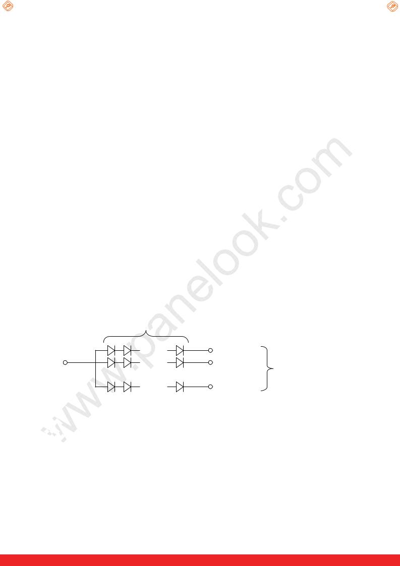
3.Each LED array has one anode terminal and 6 cathode terminals.
The forward current(IF) of the anode terminal is 630mA and it supplies 105mA into 6 strings, respectively
12 (LED Pakage / 1string)
Anode |
|
Cathode #1 |
|
Cathode #2 |
|
|
6 (LED String / 1 Array) |
|
Cathode #6 |
||
|
4. The forward voltage(VF) of LED array depends on ambient temperature (Appendix-V)
5. VF means Max VF-Min VF in one Backlight. So VF variation in a Backlight isn’t over Max. 1.7V 6.  Maximum level of power consumption is measured at initial turn on.

 Typical level of power consumption is measured after 1hrs aging at 25 ± 2 C.
7.
 The life time(MTTF) is determined as the time at which brightness of the LED is 50% compared to that of

 initial value at the typical LED current on condition of continuous operating at 25 ± 2 C, based on duty 100%
8.The reference method of burst dimming duty ratio.
It is recommended to use synchronous V-sync frequency to prevent waterfall (Vsync x 1 =Burst Frequency)
Though PWM frequency is over 182Hz (max252Hz), function of backlight is not affected.
Ver. 0.1 |
7 /43 |
|
|
PDF created with pdfFactory Pro trial version www.pdffactory.com |
www.panelook.com |
One step solution for LCD / PDP / OLED panel application: Datasheet, inventory and accessory! |

Global LCD Panel Exchange Center |
www.panelook.com |
LC550EUH
Product Specification
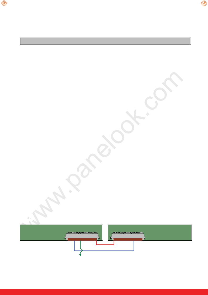
3-2. Interface Connections
This LCD module employs two kinds of interface connection, two 50-pin FFC connector are used for the module electronics and 8-pin / 8-pin connectors are used for the integral backlight system.
3-2-1. LCD Module
-LCD Connector (CN1): TF06L-50S-0.5SH (Manufactured by HRS) or Compatible
Table 3-1. MODULE CONNECTOR(CN1) PIN CONFIGURATION
No |
Symbol |
Description |
|
No |
Symbol |
Description |
|
|
|
|
|
|
|
͢ |
ͽ΅͵ΐ Ά΅ |
ͽ΅͵ Ά΅ Ά΅ |
|
ͣͧ |
GND |
Ground |
|
|
|
|
|
|
|
ͣ |
ʹ |
Π ʹΠΟΟΖΔΥΚΠΟ |
|
ͣͨ |
EPI2- |
EPI Receiver Signal(2-) |
|
|
|
|
|
|
|
ͤ |
GCLK1 |
GIP GATE Clock 1 |
|
ͣͩ |
EPI2+ |
EPI Receiver Signal(2+) |
|
|
|
|
|
|
|
ͥ |
GCLK2 |
GIP GATE Clock 2 |
|
ͣͪ |
GND |
Ground |
|
|
|
|
|
|
|
ͦ |
GCLK3 |
GIP GATE Clock 3 |
|
ͤ͡ |
GND |
Ground |
|
|
|
|
|
|
|
ͧ |
GCLK4 |
GIP GATE Clock 4 |
|
31 |
EPI1- |
EPI Receiver Signal(1-) |
|
|
|
|
|
|
|
ͨ |
GCLK5 |
GIP GATE Clock 5 |
|
32 |
EPI1+ |
EPI Receiver Signal(1+) |
|
|
|
|
|
|
|
ͩ |
GCLK6 |
GIP GATE Clock 6 |
|
33 |
GND |
Ground |
|
|
|
|
|
|
|
ͪ |
VGI_N |
GIP Bi-Scan (Normal =VGL Rotate = VGH) |
|
34 |
VCC |
Logic & EPI Power Voltage |
|
|
|
|
|
|
|
͢͡ |
VGI_P |
GIP Bi-Scan (Normal =VGH Rotate = VGL) |
|
35 |
Vterm |
·ΥΖΣΞ ΠΨΖΣ ·ΠΝΥΒΘΖ |
|
|
|
|
|
|
|
͢͢ |
VGH_ODD |
GIP Panel VDD for Odd GATE TFT |
|
36 |
LOCKOUT3 |
LOCKOUT3 |
|
|
|
|
|
|
|
ͣ͢ |
VGH_EVEN |
GIP Panel VDD for Even GATE TFT |
|
37 |
NC |
No Connection |
|
|
|
|
|
|
|
ͤ͢ |
VGL |
GATE Low Voltage |
|
38 |
GND |
Ground |
|
|
|
|
|
|
|
ͥ͢ |
VST |
VERTICAL START PULSE |
|
39 |
; ͩ͢ |
;; · ͽ΅ ͩ͢ ͙ ΦΥΡΦΥ ΣΠΞ ͽʹ͵͚ |
|
|
|
|
|
|
|
ͦ͢ |
GIP_Reset |
GIP Reset |
|
40 |
; ͧ͢ |
;; · ͽ΅ ͧ͢ |
|
|
|
|
|
|
|
ͧ͢ |
VCOM_L_FB |
VCOM Left Feed-Back Output |
|
41 |
; ͦ͢ |
;; · ͽ΅ ͦ͢ |
|
|
|
|
|
|
|
ͨ͢ |
VCOM_L |
VCOM Left Input |
|
42 |
; ͥ͢ |
;; · ͽ΅ ͥ͢ |
|
|
|
|
|
|
|
ͩ͢ |
GND |
Ground |
|
43 |
; ͣ͢ |
;; · ͽ΅ ͣ͢ |
|
|
|
|
|
|
|
ͪ͢ |
VDD |
Driver Power Supply Voltage |
|
44 |
; ͢͡ |
;; · ͽ΅ ͢͡ ͙ ΦΥΡΦΥ ΣΠΞ ͽʹ͵͚ |
|
|
|
|
|
|
|
ͣ͡ |
VDD |
Driver Power Supply Voltage |
|
45 |
; ͑ͪ |
;; · ͽ΅ ͪ ͙ ΦΥΡΦΥ ΣΠΞ ͽʹ͵͚ |
|
|
|
|
|
|
|
ͣ͢ |
H_VDD |
Half Driver Power Supply Voltage |
|
46 |
; ͑ͨ |
;; · ͽ΅ ͑ͨ |
|
|
|
|
|
|
|
ͣͣ |
GND |
Ground |
|
47 |
; ͑ͦ |
;; · ͽ΅ ͑ͦ |
|
|
|
|
|
|
|
ͣͤ |
EPI3- |
EPI Receiver Signal(3-) |
|
48 |
; ͑ͥ |
;; · ͽ΅ ͑ͥ |
|
|
|
|
|
|
|
ͣͥ |
EPI3+ |
EPI Receiver Signal(3+) |
|
49 |
; ͑ͤ |
;; · ͽ΅ ͑ͤ |
|
|
|
|
|
|
|
ͣͦ |
GND |
Ground |
|
50 |
; ͑͢ |
;; · ͽ΅ ͙͢ ΦΥΡΦΥ ΣΠΞ ͽʹ͵͚ |
|
|
|
|
|
|
|
Note :
1. Please refer to application note for details. (GIP & Half VDD & Gamma Voltage setting)
Ver. 0.1 |
8 /403 |
|
|
PDF created with pdfFactory Pro trial version www.pdffactory.com |
www.panelook.com |
One step solution for LCD / PDP / OLED panel application: Datasheet, inventory and accessory! |
Global LCD Panel Exchange Center |
www.panelook.com |
LC550EUH
Product Specification
-LCD Connector (CN1): TF06L-50S-0.5SH (Manufactured by HRS) or Compatible
Table 3-2. MODULE CONNECTOR(CN2) PIN CONFIGURATION
No |
Symbol |
Description |
|
No |
Symbol |
Description |
|
|
|
|
|
|
|
|
|
͢ |
; ͑͢ |
;; · ͽ΅ ͢ |
͙ ΦΥΡΦΥ ΣΠΞ ͽʹ͵͚ |
|
ͣͧ |
GND |
Ground |
|
|
|
|
|
|
|
|
ͣ |
; ͑ͤ |
;; · ͽ΅ ͑ͤ |
|
|
ͣͨ |
EPI1- |
EPI Receiver Signal(4-) |
|
|
|
|
|
|
|
|
ͤ |
; ͑ͥ |
;; · ͽ΅ ͑ͥ |
|
|
ͣͩ |
EPI1+ |
EPI Receiver Signal(4+) |
|
|
|
|
|
|
|
|
ͥ |
; ͑ͦ |
;; · ͽ΅ ͑ͦ |
|
|
ͣͪ |
GND |
Ground |
|
|
|
|
|
|
|
|
ͦ |
; ͑ͨ |
;; · ͽ΅ ͑ͨ |
|
|
ͤ͡ |
H_VDD |
Half Driver Power Supply Voltage |
|
|
|
|
|
|
|
|
ͧ |
; ͑ͪ |
;; · ͽ΅ ͪ |
͙ ΦΥΡΦΥ ΣΠΞ ͽʹ͵͚ |
|
31 |
VDD |
Driver Power Supply Voltage |
|
|
|
|
|
|
|
|
ͨ |
; ͢͡ |
;; · ͽ΅ ͢͡ ͙ ΦΥΡΦΥ ΣΠΞ ͽʹ͵͚ |
|
32 |
VDD |
Driver Power Supply Voltage |
|
|
|
|
|
|
|
|
|
ͩ |
; ͣ͢ |
;; · ͽ΅ ͣ͢ |
|
|
33 |
GND |
Ground |
|
|
|
|
|
|
|
|
ͪ |
; ͥ͢ |
;; · ͽ΅ ͥ͢ |
|
|
34 |
VCOM_R |
VCOM Right Input |
|
|
|
|
|
|
|
|
͢͡ |
; ͦ͢ |
;; · ͽ΅ ͦ͢ |
|
|
35 |
VCOM_R_FB |
VCOM Right Feed-Back Output |
|
|
|
|
|
|
|
|
͢͢ |
; ͧ͢ |
;; · ͽ΅ ͧ͢ |
|
|
36 |
GIP_Reset |
GIP Reset |
|
|
|
|
|
|
|
|
ͣ͢ |
; ͩ͢ |
;; · ͽ΅ ͩ͢ ͙ ΦΥΡΦΥ ΣΠΞ ͽʹ͵͚ |
|
37 |
VST |
VERTICAL START PULSE |
|
|
|
|
|
|
|
|
|
ͤ͢ |
GND |
Ground |
|
|
38 |
VGL |
GATE Low Voltage |
|
|
|
|
|
|
|
|
ͥ͢ |
LOCKOUT6 |
LOCKOUT6 |
|
|
39 |
VGH_EVEN |
GIP Panel VDD for Even GATE TFT |
|
|
|
|
|
|
|
|
ͦ͢ |
LOCKIN3 |
LOCKIN3 |
|
|
40 |
VGH_ODD |
GIP Panel VDD for Odd GATE TFT |
|
|
|
|
|
|
|
|
ͧ͢ |
Vterm |
·ΥΖΣΞ ΠΨΖΣ ·ΠΝΥΒΘΖ |
|
|
41 |
VGI_P |
GIP Bi-Scan (Normal =VGH Rotate = VGL) |
|
|
|
|
|
|
|
|
ͨ͢ |
VCC |
Logic & EPI Power Voltage |
|
42 |
VGI_N |
GIP Bi-Scan (Normal =VGL Rotate = VGH) |
|
|
|
|
|
|
|
|
|
ͩ͢ |
GND |
Ground |
|
|
43 |
GCLK6 |
GIP GATE Clock 6 |
|
|
|
|
|
|
|
|
ͪ͢ |
EPI6- |
EPI Receiver Signal(6-) |
|
44 |
GCLK5 |
GIP GATE Clock 5 |
|
|
|
|
|
|
|
|
|
ͣ͡ |
EPI6+ |
EPI Receiver Signal(6+) |
|
45 |
GCLK4 |
GIP GATE Clock 4 |
|
|
|
|
|
|
|
|
|
ͣ͢ |
GND |
Ground |
|
|
46 |
GCLK3 |
GIP GATE Clock 3 |
|
|
|
|
|
|
|
|
ͣͣ |
GND |
Ground |
|
|
47 |
GCLK2 |
GIP GATE Clock 2 |
|
|
|
|
|
|
|
|
ͣͤ |
EPI5- |
EPI Receiver Signal(5-) |
|
48 |
GCLK1 |
GIP GATE Clock 1 |
|
|
|
|
|
|
|
|
|
ͣͥ |
EPI5+ |
EPI Receiver Signal(5+) |
|
49 |
ʹ |
Π ʹΠΟΟΖΔΥΚΠΟ |
|
|
|
|
|
|
|
|
|
ͣͦ |
GND |
Ground |
|
|
50 |
ͽ΅͵ΐ Ά΅ |
ͽ΅͵ Ά΅ Ά΅ |
|
|
|
|
|
|
|
|
Note : 1. Please refer to application note for details. 
 (GIP & Half VDD & Gamma Voltage setting)
|
CN 2 |
|
Source Right PCB |
|
|
#1 |
#15 #16 |
#50 |
CN 1
#1 |
#36 |
#50 |
Source Left PCB
ͽ ʹͼͧ
ͽ΅͵ΐ Ά΅
ͽ ʹͼͤ
΄Πʹ
Ver. 0.1 |
9 /403 |
|
|
PDF created with pdfFactory Pro trial version www.pdffactory.com |
www.panelook.com |
One step solution for LCD / PDP / OLED panel application: Datasheet, inventory and accessory! |
Global LCD Panel Exchange Center |
www.panelook.com |
LC550EUH
Product Specification
3-2-2. Backlight Module
[ CN201 ] |
[ CN202 ] |
1)LED Array ass`y Connector (Plug)
:HS100-L08N-N62, (black color, manufactured by UJU)
2)Mating Connector (Receptacle)
:IS100-L08T-C46 (black color, manufactured by UJU)
1) LED Array ass`y Connector (Plug)
: HS100-L08N-N62-A (natural color, manufactured by UJU) 2) Mating Connector (Receptacle) 


: IS100-L08T-C46-A (natural color, manufactured by UJU)
Table 5. BACKLIGHT CONNECTOR PIN CONFIGURATION(CN201,CN202)
|
|
|
|
|
u |
z OjuYWYP |
|
u |
u |
z OjuYWXP |
k |
u |
|
k |
|||
X |
R6 Cathode |
slk v j |
|
|
X |
Anode_L |
slk p j |
|
|
|
sX¥s] |
|
|||||
Y |
R5 Cathode |
slk v j |
|
|
|
|
|
|
|
|
Y |
N.C |
v |
|
|||
Z |
R4 Cathode |
slk v j |
|
|
|
|||
|
|
Z |
L6 Cathode |
slk v j |
|
|||
[ |
R3 Cathode |
slk v j |
|
|
|
|||
|
|
[ |
L5 Cathode |
slk v j |
|
|||
\ |
R2 Cathode |
slk v j |
|
|
|
|||
|
|
\ |
L4 Cathode |
slk v j |
|
|||
] |
R1 Cathode |
slk v j |
|
|
|
|||
|
|
] |
L3 Cathode |
slk v j |
|
|||
^ |
N.C |
v |
|
|
|
|||
|
|
^ |
L2 Cathode |
slk v j |
|
|||
_ |
Anode_R |
slk p j |
|
|
|
|||
|
|
_ |
L1 Cathode |
|
|
|||
yX¥y] |
|
|
slk v j |
|
||||
|
|
|
|
|
||||
|
|
|
|
|
|
|
|
|

 Rear
Rear
87654321 87654321
juYWXOiP juYWYO~P
i swi
Ver. 0.1 |
10 /43 |
|
|
PDF created with pdfFactory Pro trial version www.pdffactory.com |
www.panelook.com |
One step solution for LCD / PDP / OLED panel application: Datasheet, inventory and accessory! |
Global LCD Panel Exchange Center |
www.panelook.com |
LC550EUH
Product Specification
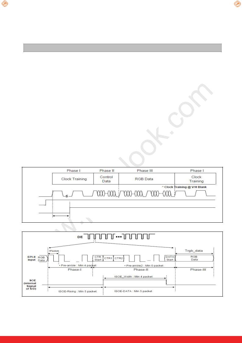
3-3. Signal Timing Specifications
Table 4. Timing Requirements
Parameter |
Symbol |
Condition |
Min |
Typ |
Max |
Unit |
Note |
|
Unit Interval |
UI |
- |
0.59(TBD) |
- |
- |
ns |
|
|
|
|
|
|
|
|
|
|
|
DLL Lock time |
Tlock |
- |
1.6(TBD) |
- |
200(TBD) |
Us |
Fig 4 |
|
|
|
|
|
|
|
|
|
|
Effective Veye width time |
B1&B2 |
- |
0.25(TBD) |
- |
- |
UI |
Fig. 2 |
|
|
|
|
|
|
|
|
|
|
SSC |
Vspread |
@100KHz |
- |
- |
2(TBD) |
% |
|
|
|
|
|
|
|
|
|
|
|
Receiver off to SOE rising time |
tSOE_ |
|
5(TBD) |
- |
- |
Packet |
Fig.5 |
|
Rising |
|
|||||||
|
|
|
|
|
|
|
||
|
|
|
|
|
|
|
|
|
SOE pulse width |
tSOE_ |
- |
4(TBD) |
- |
- |
Packet |
Fig.5 |
|
Width |
||||||||
|
|
|
|
|
|
|
||
|
|
|
|
|
|
|
|
|
SOE rising to 1st data time |
tSOE_DA |
- |
5(TBD) |
- |
- |
Packet |
Fig.5 |
|
TA |
||||||||
|
|
|
|
|
|
|
||
|
|
|
|
|
|
|
|
|
EPI Data Rate |
BW |
- |
1.251 |
- |
1.456 |
GBPS |
|
|
|
|
|
|
|
|
|
|
EPI Input
VCC
Tlock
FIG 4. Power On to DLL Lock time
FIG 5. SOE Width & Timing
Ver. 0.1 |
11 /43 |
|
|
PDF created with pdfFactory Pro trial version www.pdffactory.com |
www.panelook.com |
One step solution for LCD / PDP / OLED panel application: Datasheet, inventory and accessory! |

Global LCD Panel Exchange Center |
www.panelook.com |
LC550EUH
Product Specification
3-5. Panel Pixel Structure
D1 |
D2 |
D3 |
D4 |
D5 |
D1918 |
D1919 |
D1920 |
D1921 |
G1
G2
G3
G4
G5
G6
G1078
G1079
G1080
FIG. 8 Panel Pixel Structure
Ver. 0.1 |
12 /43 |
|
|
PDF created with pdfFactory Pro trial version www.pdffactory.com |
www.panelook.com |
One step solution for LCD / PDP / OLED panel application: Datasheet, inventory and accessory! |
Global LCD Panel Exchange Center |
www.panelook.com |
LC550EUH
Product Specification
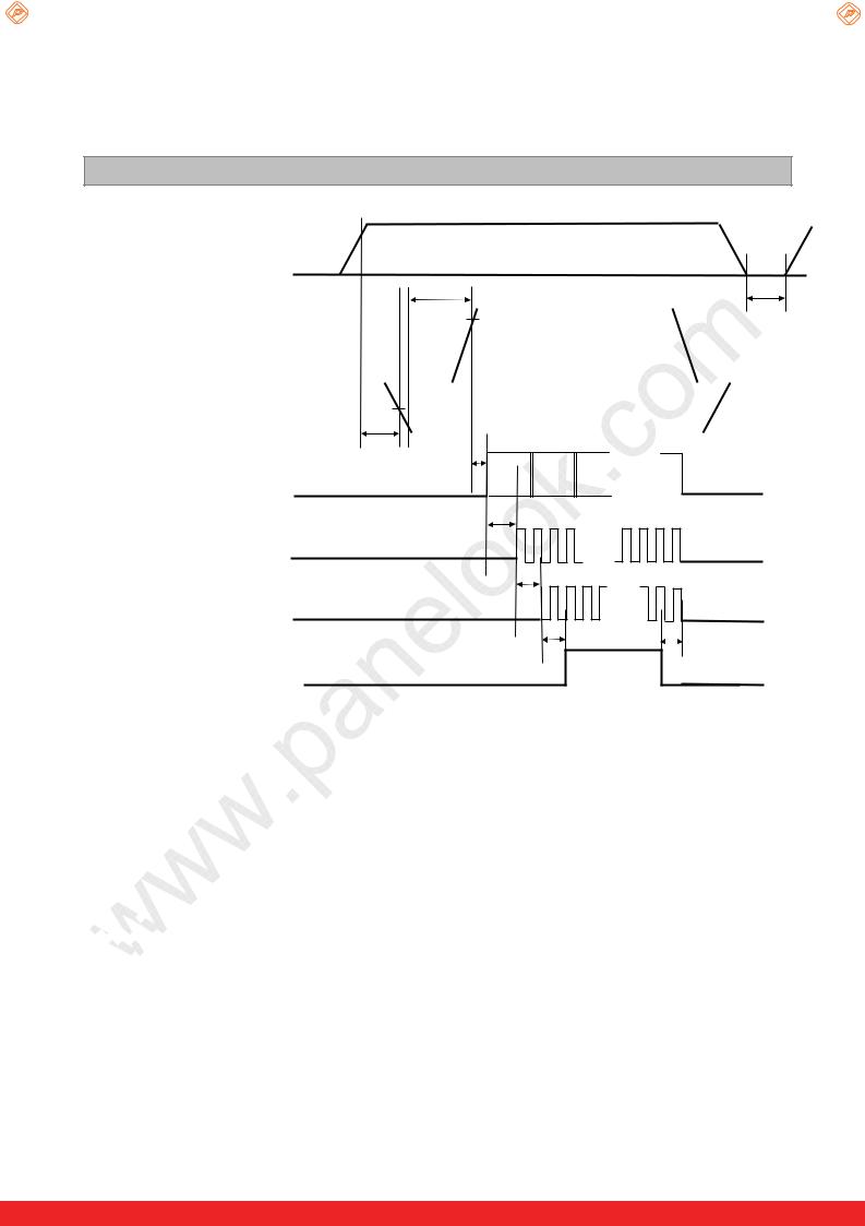
3-5. Power Sequence
3-5-1. LCD Driving circuit |
70% |
|
|
|
|
|
|
|
|
|
|
|
|
|
|
|
|||
|
|
|
|
|
|
|
|
||
Power Supply For LCD VCC |
0V |
|
|
|
|
||||
|
|
|
|
|
|||||
|
|
|
|
|
|
VGH |
|||
Power Supply For LCD |
|
|
|
|
T2 |
|
|
|
T7 |
|
|
|
|
90% |
|||||
|
|
|
|
|
|
||||
VDD, HVDD,VGH, Gamma Ref. |
|
|
|
|
|
|
|
|
|
Voltage |
|
|
|
|
|
|
|
|
|
Power Supply For LCD |
0V |
|
|
|
|
|
|
|
|
|
|
|
|
|
|
|
|
||
50% |
|
|
|
|
|
||||
VGL |
|
|
|
|
|
||||
100% |
|
|
|
|
|||||
|
|
|
|
T1 |
|
|
|
|
|
GIP Signal For LCD |
VGH |
T3 |
.. |
even/Odd |
|
||
|
|
||
|
VST |
T4 |
.. |
|
|
||
|
|
T5 |
.. |
|
|
|
|
|
GCLK1~6 |
|
|
Power For LED |
|
T6 |
T6’ |
|
|
LED on |
|
|
|
|
Table 7. POWER SEQUENCE |
|
|
Ta= 25 |
V |
||
|
|
|
|
2 C, f =120Hz, |
||
Parameter |
|
Value |
|
Unit |
|
Notes |
Min |
Typ |
Max |
|
|||
|
|
|
|
|||
T1 |
0.5 |
- |
- |
ms |
|
|
T2 |
0.5 |
- |
- |
ms |
|
|
T3 |
0 |
- |
- |
ms |
|
|
T4 |
10 |
- |
- |
ms |
|
2 |
T5 |
0 |
- |
- |
ms |
|
|
T6 / T6’ |
20 |
- |
- |
ms |
|
6 |
T7 |
2 |
- |
- |
s |
|
|
Note :  1. Power sequence for Source D-IC must follow the Case1 & 2.


 Please refer to Appendix IV for more details.

 2. VGH Odd signal should be started “High” status and VGH even & odd can not be “High at the same time.
3.Power Off Sequence order is reverse of Power On Condition including Source D-IC.
4.GCLK On/Off Sequence
Normal : GCLK4 GCLK5 GCLK6 GCLK1 GCLK2 GCLK3.
Reverse :GCLK3 GCLK2 GCLK1 GCLK6 GCLK5 GCLK4.
5.VDD_odd/even transition time should be within V_blank
6.In case of T6’, If there is no abnormal display, no problem
Ver. 0.1 |
13 /43 |
|
|
PDF created with pdfFactory Pro trial version www.pdffactory.com |
www.panelook.com |
One step solution for LCD / PDP / OLED panel application: Datasheet, inventory and accessory! |
 Loading...