


LM-W5040A
LG LM-W5040A, LM-W5040D, LM-W5040X, LM-W3140A, LM-W3140D Service Manual
...
- 1-1 -
[CONTENTS]
❍ SECTION 1.GENERAL
• SERVICING PRECAUTIONS . . . . . . . . . . . . . . . . . . . . . . . . . . . . . . . . . . . . . . . . . . . . . . . 1-2
• ESD PRECAUTIONS . . . . . . . . . . . . . . . . . . . . . . . . . . . . . . . . . . . . . . . . . . . . . . . . . . . . . 1-4
• SPECIFICATION . . . . . . . . . . . . . . . . . . . . . . . . . . . . . . . . . . . . . . . . . . . . . . . . . . . . . . . . . .1-5
❍ SECTION 2.ELECTRICAL SECTION
• TROUBLESHOOTING GUIDE . . . . . . . . . . . . . . . . . . . . . . . . . . . . . . . . . . . . . . . . . . . . . . 2-1
• INTERNAL BLOCK DIAGRAM of ICs . . . . . . . . . . . . . . . . . . . . . . . . . . . . . . . . . . . . . . . . . 2-21
• BLOCK DIAGRAM . . . . . . . . . . . . . . . . . . . . . . . . . . . . . . . . . . . . . . . . . . . . . . . . . . . . . . . 2-26
• SCHEMATIC DIAGRAMS . . . . . . . . . . . . . . . . . . . . . . . . . . . . . . . . . . . . . . . . . . . . . . . . . 2-29
• WIRING DIAGRAM . . . . . . . . . . . . . . . . . . . . . . . . . . . . . . . . . . . . . . . . . . . . . . . . . . . . . . 2-41
• PRINTED CIRCUIT BOARD DIAGRAM . . . . . . . . . . . . . . . . . . . . . . . . . . . . . . . . . . . . . . . 2-43
❍ SECTION 3. EXPLODED VIEWS . . . . . . . . . . . . . . . . . . . . . . . . . . . . . . . . . . . 3-1
❍ SECTION 4. SPEAKER PART . . . . . . . . . . . . . . . . . . . . . . . . . . . . . . . . . . . . . 4-1
❍ SECTION 5. REPLACEMENT PARTS . . . . . . . . . . . . . . . . . . . . . . . . . . . . . . . 5-1
- 1-2 -
SECTION 1. GENERAL
❏ SERVICING PRECAUTIONS
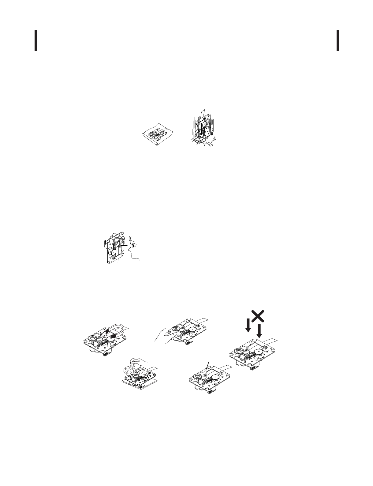
NOTES REGARDING HANDLING OF THE PICK-UP
1. Notes for transport and storage
1) The pick-up should always be left in its conductive bag until immediately prior to use.
2) The pick-up should never be subjected to external pressure or impact.
2. Repair notes
1) The pick-up incorporates a strong magnet, and so should never be brought close to magnetic materials.
2) The pick-up should always be handled correctly and carefully, taking care to avoid external pressure and
impact. If it is subjected to strong pressure or impact, the result may be an operational malfunction and/or
damage to the printed-circuit board.
3) Each and every pick-up is already individually adjusted to a high degree of precision, and for that reason
the adjustment point and installation screws should absolutely never be touched.
4) Laser beams may damage the eyes!
Absolutely never permit laser beams to enter the eyes!
Also NEVER switch ON the power to the laser output part (lens, etc.) of the pick-up if it is damaged.
5) Cleaning the lens surface
If there is dust on the lens surface, the dust should be cleaned away by using an air bush (such as used
for camera lens). The lens is held by a delicate spring. When cleaning the lens surface, therefore, a cotton
swab should be used, taking care not to distort this.
6) Never attempt to disassemble the pick-up.
Spring by excess pressure. If the lens is extremely dirty, apply isopropyl alcohol to the cotton swab. (Do
not use any other liquid cleaners, because they will damage the lens.) Take care not to use too much of
this alcohol on the swab, and do not allow the alcohol to get inside the pick-up.
Storage in conductive bag
Drop impact
NEVER look directly at the laser beam, and don’t let
contact fingers or other exposed skin.
Magnet
How to hold the pick-up
Conductive Sheet
Cotton swab
Pressure
Pressure

- 1-3 -
NOTES REGARDING COMPACT DISC PLAYER REPAIRS
1. Preparations
1) Compact disc players incorporate a great many ICs as well as the pick-up (laser diode). These components
are sensitive to, and easily affected by, static electricity. If such static electricity is high voltage, components
can be damaged, and for that reason components should be handled with care.
2) The pick-up is composed of many optical components and other high-precision components. Care must be
taken, therefore, to avoid repair or storage where the temperature of humidity is high, where strong magnet-
ism is present, or where there is excessive dust.
2. Notes for repair
1) Before replacing a component part, first disconnect the power supply lead wire from the unit
2) All equipment, measuring instruments and tools must be grounded.
3) The workbench should be covered with a conductive sheet and grounded.
When removing the laser pick-up from its conductive bag, do not place the pick-up on the bag. (This is
because there is the possibility of damage by static electricity.)
4) To prevent AC leakage, the metal part of the soldering iron should be grounded.
5) Workers should be grounded by an armband (1M Ω)
6) Care should be taken not to permit the laser pick-up to come in contact with clothing, in order to prevent sta-
tic electricity changes in the clothing to escape from the armband.
7) The laser beam from the pick-up should NEVER be directly facing the eyes or bare skin.
CLEARING MALFUNCTION
You can reset your unit to initial status if malfunction occur(button malfunction, display, etc.).
Using a pointed good conductor(such as driver), simply short the RESET jump wire on the inside of
the volume knob for more than 3 seconds.
If you reset your unit, you must reenter all its settings(stations, clock, timer)
NOTE: 1.To operate the RESET jump wire, pull the volume rotary knob and release it.
2. If you wish to operate the RESET jump wire, it is necessary to unplug the power cord.
Resistor
(1 Mohm)
Conductive
Sheet
Resistor
(1 Mohm)
Armband
RESET jump wire
VOLUME
VOLUME KNOB
DOWN
UP
- 1-4 -
❏ ESD PRECAUTIONS
Electrostatically Sensitive Devices (ESD)
Some semiconductor (solid state) devices can be damaged easily by static electricity. Such components
commonly are called Electrostatically Sensitive Devices (ESD). Examples of typical ESD devices are integrated
circuits and some field-effect transistors and semiconductor chip components.The following techniques should
be used to help reduce the incidence of component damage caused by static electricity.
1. Immediately before handling any semiconductor component or semiconductor-equipped assembly, drain off
any electrostatic charge on your body by touching a known earth ground. Alternatively, obtain and wear a
commercially available discharging wrist strap device, which should be removed for potential shock reasons
prior to applying power to the unit under test.
2. After removing an electrical assembly equipped with ESD devices, place the assembly on a conductive sur-
face such as aluminum foil, to prevent electrostatic charge buildup or exposure of the assembly.
3. Use only a grounded-tip soldering iron to solder or unsolder ESD devices.
4. Use only an anti-static solder removal device. Some solder removal devices not classified as "anti-static" can
generate electrical charges sufficient to damage ESD devices.
5. Do not use freon-propelled chemicals. These can generate electrical charges sufficient to damage ESD
devices.
6. Do not remove a replacement ESD device from its protective package until immediately before you are
ready to install it. (Most replacement ESD devices are packaged with leads electrically shorted together by
conductive foam, aluminum foil or comparable conductive materials).
7. Immediately before removing the protective material from the leads of a replacement ESD device, touch the
protective material to the chassis or circuit assembly into which the device will by installed.
CAUTION : BE SURE NO POWER IS APPLIED TO THE CHASSIS OR CIRCUIT, AND OBSERVE ALL
OTHER SAFETY PRECAUTIONS.
8. Minimize bodily motions when handing unpackaged replacement ESD devices. (Otherwise harmless motion
such as the brushing together of your clothes fabric or the lifting of your foot from a carpeted floor can gen-
erate static electricity sufficient to damage an ESD device).
CAUTION. GRAPHIC SYMBOLS
THE LIGHTNING FLASH WITH APROWHEAD SYMBOL. WITHIN AN EQUILATERAL TRIANGLE, IS
INTENDED TO ALERT THE SERVICE PERSONNEL TO THE PRESENCE OF UNINSULATED “DAN-
GEROUS VOLTAGE” THAT MAY BE OF SUFFICIENT MAGNITUDE TO CONSTITUTE A RISK OF
ELECTRIC SHOCK.
THE EXCLAMATION POINT WITHIN AN EQUILATERAL TRIANGLE IS INTENDED TO ALERT THE
SERVICE PERSONNEL TO THE PRESENCE OF IMPORTANT SAFETY INFORMATION IN SERVICE
LITERATURE.
- 1-5 -
❏ SPECIFICATIONS
[General][CD]
[Tuner]
AM
FM
(MW)
[Amp]
[
TAPE
]
Power supply Refer to the back panel of the unit.
Power consumption 220W 170w 150w 110w
Mass 12kg 10kg 10kg
External dimensions (W x H x D) 280 x 370 x 372 mm
Frequency response 40 - 18000 Hz
Signal-to-noise ratio 70 dB
Dynamic range 70 dB
Tuning Range 87.5 - 108.0 MHz or 65 - 74 MHz
Intermediate Frequency 10.7 MHz
Signal to Noise Ratio 60/55 dB
Frequency Response 60 - 10000 Hz
Tuning Range 522 - 1611 kHz or 530 - 1610 kHz
Intermediate Frequency 450 kHz
Signal to Noise Ratio 35 dB
Frequency Response 120 - 2000 Hz
Output Power 310W + 310W 230W + 230W 310W + 310W 230W + 230W
T.H.D 0.7%
Frequency Response 42 - 25000 Hz
Signal-to-noise ratio 75 dB
Tape Speed 4.75cm/sec
Wow Flutter 0.25% (MTT -111, JIS-WTD)
F.F/REW Time 120sec (C-60)
Frequency Response 125 - 8000Hz
Signal to Noise Ratio 43dB
Channel Separation 50dB(P/B)/45dB(R/P)
Erase Ratio 55dB (MTT-5511)
Designs and specifications are subject to change without notice.
LM-W5040A/D/X
LM-W3140A/D/X
MODEL
SECTION
LM-W4040A/D/X
LM-W2340A/D/X
[Front Speakers]
Model name LMS-W5040 LMS-W4040 LMS-W3140 LMS-W2340
Type
3Way 4Speaker 3Way 4Speaker 3Way 4Speaker 3Way 4Speaker
Impedance 6Ω 6Ω 6Ω 6Ω
Frequency Response 45-20000Hz 45-20000Hz 45-20000Hz 45-20000Hz
Sound Pressure Level 85dB 85dB 85dB 85dB
Rated Input Power 250W 230W 310W 230W
Max. Input Power 500W 460W 620W 460W
Net Dimensions(WxHxD) 255x425x300 255x425x300 255x425x300 255x425x300
Net Weight 10.4 10.4 10.4 10.4
Model name LMS-W5040S
Type 2Way 3Speak
24Ω
er
Impedance
Frequency Response 60-20000Hz
Sound Pressure Level 85dB
Rated Input Power 100W
Max. Input Power 200W
Net Dimensions(WxHxD) 187 x 425 x 248
Net Weight 5.3
[Surround Speakers]
Model name LMS-W5040W, LMS-W4040W
Type 1W
6Ω
ay 1Speaker
Impedance
Frequency Response 40-15000Hz
Sound Pressure Level 83dB
Rated Input Power 310W
Max. Input Power 620W
Net Dimensions(WxHxD) 255 x 425 x 300
Net Weight 9.2
[Woofer Speakers]
, 87.5 - 108.0 MHz
12kg

- 1-6 -

- 2-1 -
SECTION 2. ELECTRICAL
■ CD PART
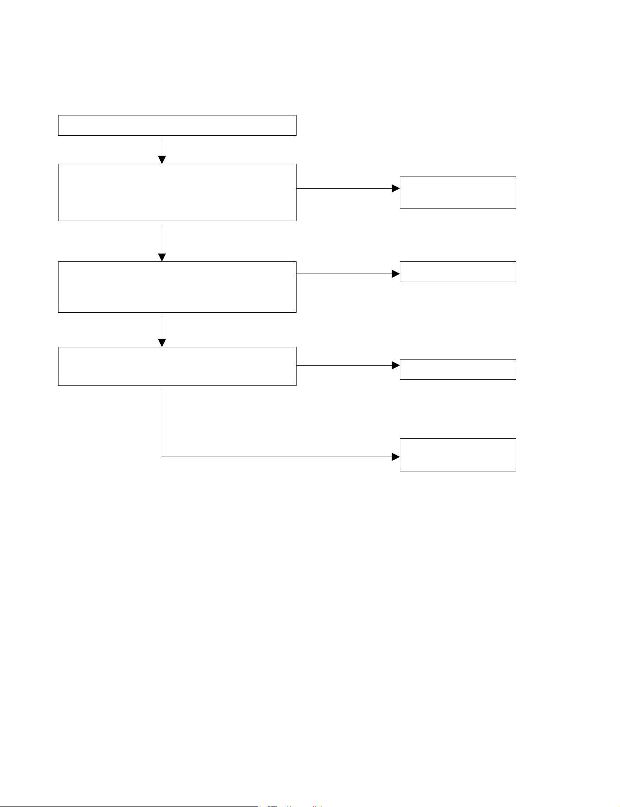
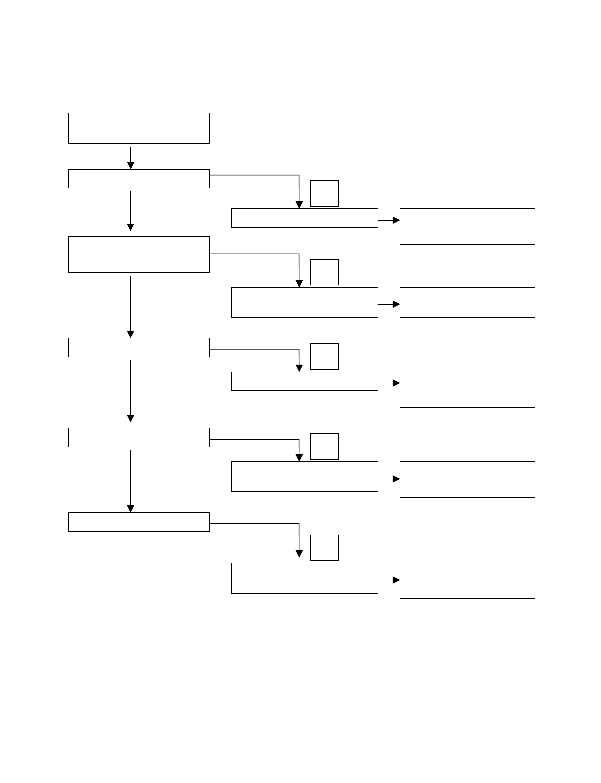
❏ TROUBLESHOOTING GUIDE
TURN ON CD
CONNECTOR CHECK ( PN808,PN807 )
CHECK POWER SUPPLY CIRCUIT( PN808 )
CHECK MICOM INTERFACE CIRCUIT( PN807 )
CHECK MICOM INTERFACE CIRCUIT( PN807 )
CONNECTOR CHECK(PN801,PN802)
CHECK PICKUP MOVEMENT
CHECK BA5810FP (IC803)
CHECK MN6627933CG (IC801)
CHECK AN22004 (IC802)
CONNECTOR CHECK (PN808)
CONNECTOR CHECK
( PN808,PN807,PN802,PN801 )
OPEN CLOSE CHECK
“ READING ”
DISPLAY CHECK
READING OK CHECK
IF PLAY, AUDIO
OUTPUT CHECK
OK
NO
NO
NO
NO
YES
YES
YES
YES
YES
- 2-2 -
CONNECTOR LOCKING CHECK ( PN808,PN807 )
DEFECTIVE MAIN
POEWR SUPPLY
DEFECTIVE MICOM
DEFECTIVE IC803
DEFECTIVE
MECHANISM
CHECK POWER SUPPLY CIRCUIT( PN808 ,PN807)
PN808 PIN 5 = 6.2V, PIN 7 = 5V
PN807 PIN 1 = 5V
CHECK VOLTAGE CHANGE OF OPEN CLOSE ,
AND BTLMUTE VOLTAGE(= 5V)
(PN807 PIN 20:OPEN, 19:CLOSE, 4:BTLMUTE)
CHECK VOLTAGE CHANGE LO+, LO- OF IC803
(PN807, PIN OPEN:20, CLOSE:19)
YES
YES
YES
NO
NO
NO
NO
• OPEN CLOSE NG

- 2-3 -
CONNECTOR LOCKING CHECK
(PN808,PN807,PN802,PN801 )
DEFECTIVE CONNECTOR OR
MAIN POWER SUPPLAY
DEFECTIVE IC805
DEFECTIVE MICOM OR
CONNECTOR
DEFECTIVE MICOM OR
CONNECTOR
DEFECTIVE IC801
CHECK VOLTAGE THE PIN 2 OF IC805
IC805 PIN2 : 3.3V
CHECK RESET SIGNAL OF PN807
PN807 PIN12 : 5V
CHECK POWER SUPPLY
PORT( PN808 ,PN807)
PN808 PIN 5 = 6.2V, PIN 7 = 5V
PN807 PIN 1 = 5V
CHECK POWER SUPPLY
PORT( PN808 ,PN807)
PN808 PIN 5 = 6.2V, PIN 7 = 5V
PN807 PIN 1 = 5V
CHECK MICOM INTERFACE
CIRCUIT( PN807 )
PN807 PIN 11,13,14,15 SIGNAL CHECK
(11: STAT, 13: MDATA, 14:MCLK, 15:MLD)
CHECK THE WAVE FORM #1
YES
YES
YES
YES
YES
NO
NO
NO
NO
NO
• “ READING ” DISPLAY CHECK (= ONLY “CD “DISPLAY)
- 2-4 -
A
B
C
D
E
CONNECTOR LOCKING
CHECK(PN801,PN802)
DOES SLED MOVE ?
CHECK PN802 PIN 3,4( SL+,SL-)
DEFECTIVE PICKUP OR
IC803 OR IC801 OR IC802
DEFECTIVE PICKUP OR
IC803 OR IC801 OR IC802
DEFECTIVE PICKUP OR
IC803 OR IC801
DEFECTIVE PICKUP OR
IC802
DEFECTIVE PICKUP OR
IC803
DEFECTIVE PICKUP OR
IC803 OR IC801 OR IC802
CHECK PN802 PIN 10( LD )
CHECK PN801 PIN 14,15
(TA- ,TA+)
CHECK PN802 PIN
5,6( SP+,SP-)
CHECK PN801 PIN 13,16
( FA-, FA+)
DOES LENSE MOVE ?
(= UP & DOWN)
DOES LASER LIGHT ?
DOES SPINDLE ROTATE ?
IS READING OK ?
YES
YES
YES
YES
YES
NO
NO
NO
NO
NO
• READING OK CHECK (= “NO DISC” DISPLAY)

- 2-5 -
CHECK PN802 CONNECTOR LINE
DEFECTIVE IC801
DEFECTIVE IC803
DEFECTIVE PN802
CONNECTOR
DEFECTIVE PICKUP
SLED MOTOR
A
DOES SL+ WAVEFORM APPEAR AT
( IC803 PIN14 AND PN802 PIN3)
WAVEFORM #2
SLED MOTOR WAVE
DOES SLIN WAVEFORM
APPEAR AT
( IC803 PIN 5)
WAVEFORM #2
SLED DRIVE WAVE
YES
YES
NO
NO
NO
NO
NO
• READING OK CHECK #A (= “NO DISC” DISPLAY)

- 2-6 -
CHECK PN801 CONNECTOR LINE
DEFECTIVE IC801
DEFECTIVE IC803
DEFECTIVE PN801
CONNECTOR
DEFECTIVE PICKUP
FOCUS ACTUATOR
B
DOES FA+ WAVEFORM APPEAR AT
( IC803 PIN15 AND PN801 PIN16)
WAVEFORM #3
FOCUS COIL DRIVE WAVE
DOES FAIN- WAVEFORM
APPEAR AT
( IC803 PIN 26)
WAVEFORM #3
FOCUS DRIVE WAVE
YES
YES
NO
NO
NO
NO
NO
• READING OK CHECK #B (= “NO DISC” DISPLAY)
- 2-7 -
CHECK PN801 CONNECTOR LINE
DEFECTIVE IC805
DEFECTIVE IC802
DEFECTIVE Q801 OR
D811
DEFECTIVE PN801
CONNECTOR
DEFECTIVE PICKUP
LASER PART
C
IS ?V APPLIED TO PIN10 OF
PN801
LASER SUPPLY VOLTAGE CHECK
IS 3.3 V APPLIED TO
PIN3 OF IC802
RF IC SUPPLY VOLTAGE
CHECK
IS 2.0 V PIN2 OF IC802
LASER CONTROL
VOLTAGE CHECK
YES
YES
NO
NO
NO
NO
NO
NO
• READING OK CHECK #C (= “NO DISC” DISPLAY)

- 2-8 -
CHECK PN802 CONNECTOR LINE
DEFECTIVE IC801
DEFECTIVE IC803
DEFECTIVE PN802
CONNECTOR
DEFECTIVE PICKUP
SPINDLE MOTOR
D
DOES SP+ WAVEFORM APPEAR AT
( IC803 PIN12 AND PN802
PIN6)WAVEFORM #4
SPINDLE MOTOR DRIVE WAVE
DOES SPIN WAVEFORM
APPEAR AT( IC803 PIN 6)
WAVEFORM #4
SPINDLE DRIVE WAVE
YES
YES
NO
NO
NO
NO
• READING OK CHECK #D (= “NO DISC” DISPLAY)
- 2-9 -
CHECK PN802 CONNECTOR LINE
DOES ARF SIGNAL APPEAR?
(IC802 PORT 8)
WAVEFORM #6
DOES FE, TE SIGNAL APPEAR?
(IC802 PORT FE:23, TE:21)
WAVEFORM #6
DEFECTIVE IC801
DEFECTIVE IC803
DEFECTIVE PN802
CONNECTOR
DEFECTIVE PICKUP OR
IC802
DEFECTIVE PICKUP OR
IC802
DEFECTIVE IC801
E
DOES TA+ WAVEFORM APPEAR AT
( IC803 PIN17 AND PN801 PIN15)
WAVEFORM #5
TRACKING COIL DRIVE WAVE
DOES TAIN- WAVEFORM
APPEAR AT
( IC803 PIN 23)
WAVEFORM #5
TRACKING DRIVE WAVE
YES
YES
YES
NO
NO
NO
NO
NO
NO
NO
• READING OK CHECK #E (= “NO DISC” DISPLAY)
- 2-10 -
■ AUDIO PART
P-SENS PART CHECK
ZD 701(+) Voltage check
IC301 26PIN PATTERN Check
Half-wave rectification wave form check
R746 check, then ZD701 replacement
D713 Replacement
VKK CHECK
CN305 4pin DC -33V check
IC301 51PIN check
ZD 700 -33V check
ZD 754 turn on check
Pattern disconnection check
D707, D708 replacement
normal
ZD700 replacement
Refer to power
supply check
C763 -33V and less check
Q754 replacement

- 2-11 -
POWER CHECK
Every kinds of Fuse check
C720(+), C770(-) DC power output check
C725(+), C729(-) DC power output check
IC704, IC705, IC705 power output check
IC704, IC705, IC710 power output check (12V)
IC709 DC5V check
CN513 7PIN 5V check (at CD Function)
normal operation
Fuse replace
CN704 1, 2, 3, 4, 5, 6, 7, 9, 10 AC voltage output check
D713(PBU604) check
Power supply Ass’y check
and transformer replacent
IC301 5V Power output
PN304/CN304 15 PIN check
Check
IC5019BU2090 check & replace
IC501(BU2090) 14PIN HIGH check
Check and replace defective
Power supply Ass’y check
and transformer replacent
CN704, 11, 12 pin AC power output check
IC704, IC705 , IC710 check and replacement
IC301 78PIN 5V check
IC709 replacement
Q904(A1273) Base Low check
Q904, CD Ass’y check replacement
- 2-12 -
Muting circuit Troubleshooting (if MUTE)
Q752(A102) Base “LOW”
C720(+), C770(-) DC power output check
MUTE
c-COM operation status check
Each appropriate TR replacement
Check each function input and operation
status check
Refer to IC601(TDA7429D) IC specification
c-COM check (and CLK/DATA check)
IC705 7812 operation status check (DC12V)
PN701/CN701 connection status check
ZD601 9.1V check
IC601 39PIN (over 8V) check and power
supply circuit check
Q702(A102) operation status check
Q702(A102) Replace if defective
c-COM 2PIN(A-MUTE)
LINE check
No sound
Input check (AUX➞29,36 TUNER➞30,35
TAPE➞28/37 CD➞31/34 PIN)
IC 601 24/25 PIN Output check
IC601 input check (22/21PIN)
IC601 output check (14PIN)
normal
 Loading...