


 Loading...
VHF FM TRANSCEIVER
TM-271A/271E
SERVICE MANUAL
© 2003-10 PRINTED IN JAPAN B51-8663-00 (N) 743
TM-271A (M2,M4)
Key top
(K29-9291-01)
Microphone Knob (Volume) (T91-0624-05) (K29-9292-03)
Cabinet (A01-2193-01)
Knob (Encoder) (K29-9293-03)
Panel assy (A62-1088-03)
TM-271A/E (K,M3,E)
Key top
(K29-9291-01)
Microphone Knob (Volume) (T91-0641-05) (K29-9292-03)
Cabinet (A01-2193-01)
Knob (Encoder) (K29-9293-03)
Panel assy (A62-1088-03)
CONTENTS
CIRCUIT DESCRIPTION ............................ |
2 |
SEMICONDUCTOR DATA ........................ |
8 |
COMPONENTS DESCRIPTION ................ |
9 |
PARTS LIST ............................................. |
10 |
EXPLODED VIEW.................................... |
17 |
PACKING ................................................. |
18 |
RESETTING THE TRANSCEIVER ........... |
19 |
ADJUSTMENT ........................................ |
20 |
TERMINAL FUNCTION ........................... |
|
27 |
PC BOARD |
|
|
DISPLAY UNIT (X54-3450-10) ............ |
28 |
|
TX-RX UNIT (X57-685X-XX) ............... |
30 |
|
SCHEMATIC DIAGRAM .......................... |
|
34 |
BLOCK DIAGRAM ................................... |
|
38 |
LEVEL DIAGRAM .................................... |
|
40 |
SPECIFICATION ................... |
BACK COVER |
|

TM-271A/271E
CIRCUIT DESCRIPTION
Frequency Configuration
The receiver utilizes double conversion. The first IF is 49.95MHz and the second IF is 450kHz. The first local oscillator signal is supplied from the PLL circuit.
The PLL circuit in the transmitter generates the necessary frequencies. Figure 1 shows the frequencies.
ANT |
|
|
|
|
|
|
|
|
|
|
|
|
|
|
CF 450kHz |
|
|
|
|
|
||||||||||
|
|
|
|
|
|
|
|
|
|
1st |
|
|
MCF |
|
|
|
|
|
|
|
|
|
|
|
|
|
||||
|
|
|
|
|
|
|
|
|
|
|
|
|
|
|
|
|
|
|
|
|
|
|
|
|
||||||
|
|
|
|
|
|
|
|
|
MIX 49.95MHz |
|
|
|
|
|
|
|
|
|
|
|
|
|
||||||||
ANT |
|
|
|
RF |
|
|
|
|
|
|
|
|
|
|
|
IF SYSTEM |
|
|
AF |
|
|
|
SP |
|||||||
|
|
|
|
|
|
|
|
|
|
|
|
|
|
|
|
|
|
|
||||||||||||
SW |
|
|
AMP |
|
|
|
|
|
|
|
|
|
|
|
|
|
PA |
|
|
|
||||||||||
|
|
|
|
|
|
|
|
|
|
|
|
|
|
|
|
|
|
|
|
|
|
|
|
|
||||||
|
|
|
|
|
|
|
|
|
|
|
|
|
|
|
|
|
|
|
|
|
50.4MHz |
|
|
|
|
|
||||
|
|
|
|
|
|
|
|
|
|
|
|
|
|
|
|
|
|
|
|
|
|
|
|
|
|
|||||
|
|
|
|
|
|
|
|
|
|
|
|
|
|
|
|
|
|
|
|
|
|
|
|
|
|
|
|
|
|
|
|
|
|
|
|
|
|
|
|
|
|
|
|
|
|
|
|
|
|
|
X3 |
|
|
|
|
|
|
|
|
||
|
|
|
|
|
|
|
|
|
|
|
|
|
|
|
|
|
|
|
multiply |
|
|
|
|
|
|
|
|
|||
|
|
|
|
|
|
|
|
|
|
|
|
|
|
|
|
|
|
|
|
|
|
|
16.8MHz |
|
|
|
|
|||
|
|
|
|
|
|
|
|
|
|
|
|
|
|
|
|
|
|
|
TCXO |
|
|
|
|
|||||||
|
|
|
|
|
|
|
|
|
|
|
|
RX |
|
|
|
|
|
|
|
|
|
|
|
|
|
|
|
|
||
|
|
|
|
|
|
|
|
|
|
|
|
|
|
|
|
|
|
|
|
|
|
|
|
|
|
|
|
|||
|
|
|
|
|
|
|
|
|
|
|
|
|
|
|
|
|
|
|
|
|
|
|
|
|
|
|
|
|||
|
|
|
|
|
|
|
|
|
|
|
|
1/2 |
|
PLL/VCO |
|
|
MIC |
|
|
|
MIC |
|||||||||
POWER |
|
|
RF |
|
|
|
|
|
|
|
|
|
|
|
AMP |
|
|
|
||||||||||||
|
|
|
|
|
|
|
|
|
|
|
|
|
|
|||||||||||||||||
AMP |
|
|
AMP |
|
|
|
TX |
|
|
|
|
|
|
|
|
|
|
|
|
|
|
|
||||||||
|
|
|
|
|
|
|
|
|
|
|
|
|
|
|
|
|
|
|
|
|
||||||||||
■ IF Amplifier
The first IF signal is amplified by Q351, and then goes to IC301 (FM processing IC). The signal is heterodyned again with a second local oscillator signal within IC301 to create a 450kHz second IF signal. The second IF signal is then fed through a 450kHz ceramic filter (Wide : CF301, Narrow : CF302) to further eliminate unwanted signals before it is amplified and FM detected in IC301.
Item |
Rating |
|
|
Nominal center frequency |
49.95MHz |
|
|
Pass bandwidth |
± 5.0kHz or more at 3dB |
|
|
35dB stop bandwidth |
± 20.0kHz or less |
|
|
Ripple |
1.0dB or less |
|
|
Insertion loss |
5.0dB or less |
|
|
Guaranteed attenuation |
80dB or more at fo± 1MHz |
|
|
Spurious |
40dB or more |
|
|
Terminal impedance |
350Ω / 5.5pF |
Fig. 1 Frequency configuration
Receiver System
The receiver is double conversion superheterodyne. The frequency configuration is shown in Figure 1.
■ Front-end RF Amplifier
An incoming signal from the antenna is applied to an RF amplifier (Q353) after passing through a transmit/receive switch circuit (D603, D605 are off) and a band pass filter (L357, L356 and varactor diodes : D353, D354). After the signal is amplified (Q353), the signal is filtered through a band pass filter (L354, L355 and varactor diodes: D351, D352) to eliminate unwanted signals before it is passed to the first mixer.
The voltage of these diodes are controlled by tracking the CPU (IC101) center frequency of the band pass filter. (See Fig. 2.)
■ First Mixer
The signal from the RF amplifier is heterodyned with the first local oscillator signal from the PLL frequency synthesizer circuit at the first mixer (Q352) to create a 49.95MHz first intermediate frequency (1st IF) signal. The first IF signal is then fed through one pair of monolithic crystal filter (MCF : XF351) to further remove spurious signals.
Table 1 Crystal filter (L71-0620-05) : XF351
Item |
Rating |
|
|
Nominal center frequency |
450kHz |
|
|
6dB bandwidth |
± 6.0kHz or more |
|
|
50dB bandwidth |
± 12.5kHz or less |
|
|
Ripple |
2.0dB or less |
|
|
Insertion loss |
6.0dB or less |
|
|
Guaranteed attenuation |
35.0dB or more within fo± 100kHz |
|
|
Terminal impedance |
2.0kΩ |
|
|
Table 2 Ceramic filter (L72-0993-05) : CF301 |
|
Item |
Rating |
|
|
Nominal center frequency |
450kHz |
|
|
6dB bandwidth |
± 4.5kHz or more |
|
|
50dB bandwidth |
± 10.0kHz or less |
|
|
Ripple |
2.0dB or less |
|
|
Insertion loss |
6.0dB or less |
|
|
Guaranteed attenuation |
60.0dB or more within fo± 100kHz |
|
|
Terminal impedance |
2.0kΩ |
|
|
Table 3 Ceramic filter (L72-0999-05) : CF302
|
|
|
|
|
|
|
|
|
|
|
|
|
|
|
|
|
|
|
|
|
|
|
|
|
|
|
|
|
|
|
|
|
CF301 (Wide) |
|||||||||
ANT |
|
|
|
|
|
|
|
|
|
|
|
|
|
|
|
|
|
|
|
|
|
|
|
|
|
|
|
|
|
|
|
|
|
|
|
|
||||||
|
|
|
|
|
|
|
|
|
|
|
|
|
|
|
|
|
|
|
|
|
|
|
|
|
|
CF302 (Narrow) |
||||||||||||||||
|
|
|
D602 |
|
L357,356 |
|
|
|
|
L354,355 |
|
|
|
|
|
|
|
|
|
|
|
|
||||||||||||||||||||
|
|
|
|
|
Q353 |
Q352 |
XF351 |
|
|
Q351 |
|
|
|
|
|
|
|
IC161 |
||||||||||||||||||||||||
|
|
|
D603 |
|
D353,354 |
|
D351,352 |
|
|
|
|
|
|
|
|
|
||||||||||||||||||||||||||
|
|
|
D605 |
|
|
|
BPF |
RF AMP |
|
BPF |
MIX |
|
MCF |
|
IF AMP |
|
|
|
|
|
|
D/A CONVERTER |
||||||||||||||||||||
|
|
|
ANT |
|
|
|
|
|
|
|
|
|
|
|
|
|
|
|
|
|
|
|
|
|
|
|
|
|
|
|
|
IC301 |
|
|
|
|
|
|||||
|
|
|
SW |
|
|
|
|
|
|
|
|
|
|
|
|
|
|
|
|
|
|
|
|
|
|
|
|
|
|
|
|
IF system |
|
|
|
|
|
|||||
|
|
|
|
|
|
|
|
|
|
|
|
|
|
|
|
|
|
|
|
|
|
|
|
|
|
|
|
|
|
|
|
|
|
W/NO |
||||||||
|
|
|
|
|
|
|
|
|
|
|
|
|
|
|
|
|
|
|
|
|
|
|
|
|
|
|
|
|
|
|
|
|
|
|
|
|
|
|
|
|
||
|
|
|
|
|
|
|
|
|
|
|
|
|
|
|
|
|
|
|
|
|
|
|
|
|
|
|
|
|
|
|
|
|
|
|
|
|
|
|
||||
|
|
|
|
|
|
|
|
|
|
|
|
|
|
|
|
|
|
|
|
|
|
|
|
|
|
|
|
|
|
|
|
|
|
|
|
|
|
|
|
(EVOL2) |
||
|
|
|
|
|
|
|
|
|
|
|
|
|
|
|
|
|
|
|
|
|
|
|
|
|
|
|
|
|
|
|
|
|
|
|
|
|
|
|
|
|||
|
|
|
|
|
|
|
|
|
|
TV |
|
|
|
|
|
|
|
|
IC402 |
|
|
|
|
X401 |
|
Q302 |
|
|
|
|
|
|
||||||||||
|
|
|
|
|
|
|
|
|
|
|
|
|
|
|
|
|
|
|
|
|
|
|
|
|
|
|
|
|
|
|
|
|||||||||||
|
|
|
|
|
|
|
|
|
|
|
|
|
|
|
|
|
|
|
|
|
1/2 divider |
|
|
TCXO |
|
|
X3 multiply |
|
|
|
|
|
|
|||||||||
|
|
|
IC203 |
|
|
|
IC161 |
|
|
CPU |
|
|
|
|
|
|
|
|
|
|
|
|
|
|
|
|
|
|
|
|
|
|
|
|
|
|
||||||
|
|
|
|
|
|
|
|
|
|
|
|
|
|
|
|
|
|
|
|
|
|
|
|
|
|
|
|
|
|
|
|
|
|
|||||||||
|
|
|
DC AMP |
|
|
|
|
D/A |
|
|
|
|
|
|
1st local |
|
|
|
|
|
|
|
|
|
|
|
|
|
|
|
|
|
|
|
||||||||
|
|
|
|
|
|
|
|
|
|
|
|
|
|
|
|
|
|
|
|
|
|
|
|
|
|
|
|
|
|
|
|
|
|
|||||||||
|
|
|
|
|
|
|
|
|
|
|
|
|
|
|
|
|
|
|
OSC (VCO/PLL) |
|
|
|
|
|
|
|
|
|
|
|
|
|
|
|
|
|||||||
Fig. 2 Receiver system
2
TM-271A/271E
CIRCUIT DESCRIPTION
■ Wide/Narrow Switching Circuit
The Wide port (pin 65) and Narrow port (pin 64) of the CPU is used to switch between ceramic filters. When the Wide port is high, the ceramic filter SW diodes (D303, D302) cause CF301 to turn on to receive a Wide signal.
When the Narrow port is high, the ceramic filter SW diodes (D303, D302) cause CF302 to turn on to receive a Narrow signal. (See Fig. 3.)
|
IC301 |
IF_IN |
IF System |
MIX_O |
|
|
R318 |
CF301 |
Wide |
IC101 65pin |
|
(Wide) |
R317 |
|
|
CF302 |
|
D303 |
(Narrow) |
D302 |
R320 |
R319 |
Narrow
IC101 64pin
Fig. 3 Wide/Narrow switching circuit
■ AF Signal System
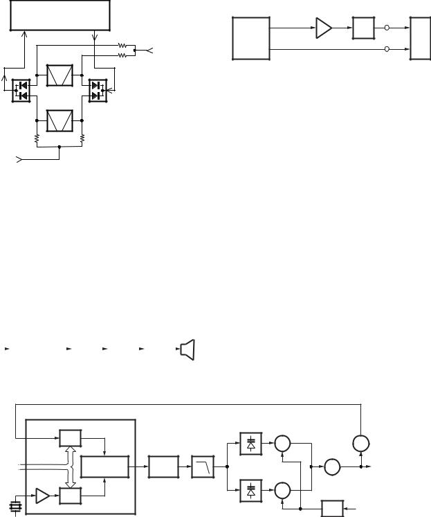
The detection signal from IF IC (IC301) goes to D/A converter (IC161) to adjust the gain and is output to AF filter (IC251) for characterizing the signal. The AF signal output from IC251 and the DTMF signal, BEEP signal are summed and the resulting signal goes to the D/A converter (IC161). The AFO output level is adjusted by the D/A converter. The signal output from the D/A converter is input to the audio power amplifier (IC252). The AF signal from IC252 switches between the internal speaker and speaker jack (J1) output. (See Fig. 4.)
IC301 |
IC161 |
W/NO |
IC251 |
|
|
IC161 |
|
|
IC252 |
|
SP |
||||
IF IC |
|
|
D/A |
(EVOL2) |
AF |
|
|
D/A |
|
|
AF PA |
|
|
|
|
|
|
|
|
|
|
|
|
|
|||||||
|
|
CONV. |
|
|
Filter |
|
|
CONV. |
|
|
|
|
|
||
|
|
|
|
|
|
|
|
|
|
|
|
|
|||
|
|
|
|
|
|
|
|
|
|
|
|
|
|
|
|
Fig. 4 AF signal system
■ Squelch Circuit
The detection output from the FM IF IC (IC301) passes through a noise amplifier (Q301) to detect noise. A voltage is applied to the CPU (IC101). The CPU controls squelch according to the voltage (SQIN) level. The signal from the RSSI pin of IC301 is used for S-meter. The electric field strength of the receive signal can be known before the SQIN voltage is input to the CPU, and the scan stop speed is improved.
|
Q301 |
|
IC301 |
NOISE AMP D301 |
IC101 |
AFO |
SQIN |
|
IF |
DET |
|
|
CPU |
|
SYSTEM RSSI |
RSSI |
Fig. 5 Squelch circuit
PLL Frequency Synthesizer
The PLL circuit generates the first local oscillator signal for reception and the RF signal for transmission.
■ PLL
The frequency step of the PLL circuit is 5 or 6.25kHz. A 16.8MHz reference oscillator signal is divided at IC401 by a fixed counter to produce the 5 or 6.25kHz reference frequency. The voltage controlled oscillator (VCO) output signal is buffer amplified by Q410, then divided in IC401 by a dualmodule programmable counter. The divided signal is compared in phase with the 5 or 6.25kHz reference signal in the phase comparator in IC401. The output signal from the phase comparator is filtered through a low-pass filter and passed to the VCO to control the oscillator frequency. (See Fig. 6.)
■ VCO
The operating frequency is generated by Q406 in transmit mode and Q405 in receive mode. The oscillator frequency is controlled by applying the VCO control voltage, obtained from the phase comparator, to the varactor diodes (D405 and D406 in transmit mode and D403 and D404 in receive mode). The TX/RX pin is set high in receive mode causing Q408 and Q407 to turn Q406 off, and turn Q405 on. The TX/RX pin is set low in transmit mode. The outputs from Q405 and Q406 are amplified by Q410 and sent to the RF amplifiers. (See Fig. 6.)
IC401 : PLL IC
|
|
|
Q406 |
Q404 |
|
|
5kHz/6.25kHz |
|
TX VCO |
AMP |
|
|
1/N |
|
|
Q410 |
|
|
|
Q402,403 |
LPF |
BUFF |
|
|
|
AMP |
|||
|
Phase |
Charge |
D405,406 |
||
PLL |
RF amplifiers |
||||
Q405 |
|||||
DATA |
comparator |
pump |
|||
|
|||||
|
REF |
|
RX VCO |
|
|
|
OSC |
|
|
Q407,408 |
|
|
1/M |
|
|
T/R SW |
|
|
5kHz/6.25kHz |
|
D403,404 |
TX/RX (CPU) |
|
|
|
|
|||
|
|
|
|
||
16.8MHz |
|
|
|
|
Fig. 6 PLL circuit
3
Loading...